High Power Switch - High Side vs. Low Side Switching
Imagine a battery pack with <=60VDC of maximum voltage and a load of up to 10kW of power(the PMSM inverter with the input capacitance of up to 1mF). The load is not always known - could be 100uF-1000uF input capacitance while the currents usually range from 20A up until 150A. The load is switched on/off using N channel Mosfets. Since there is no galvanic isolation present in the system peripheral communication interfaces(i.e. RS485/CAN) share the same GND as the load.
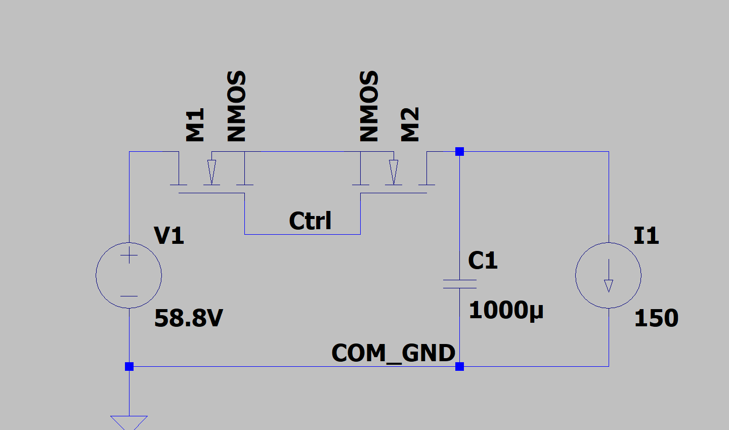
Approach 1)
Approach 2)
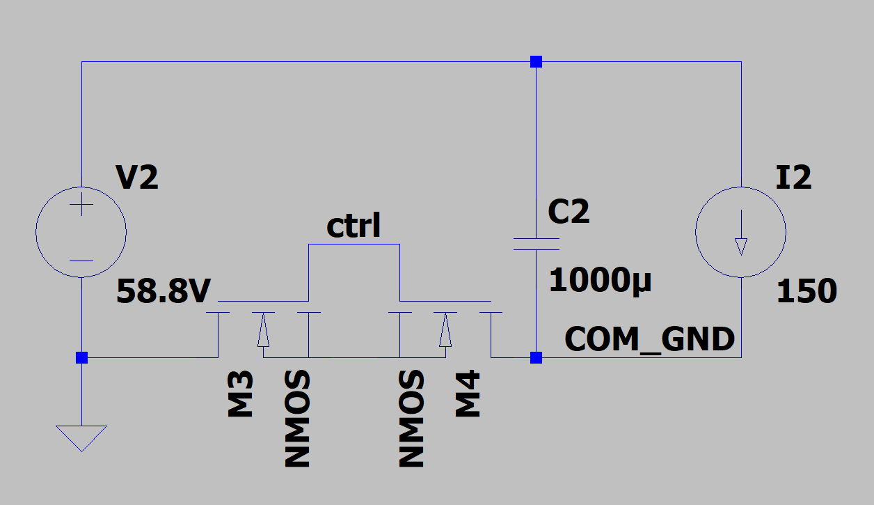
Note: Precharge circuit is present but omitted from the schematic
-
Is there a superior architecture approach in this case?
-
Could "Approach 2)" harm any of the components due to the ground reference loss?
2 answers
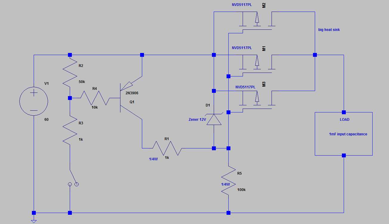
Answer to question 1: First, you need p-mos and not n-mos, as you are switching the circuit from the above. Second, it is better and simpler to parallelize mosfets for big current switches; this will reduce the power dissipation as well.
So, even if there exist a pmos with 150A ability (which I'm not sure), it is probably better and less expensive to parallelize 3 p-mos (say) of 60A. The NVD5117PL 60V, 60A, is an option. Here is the schematic:
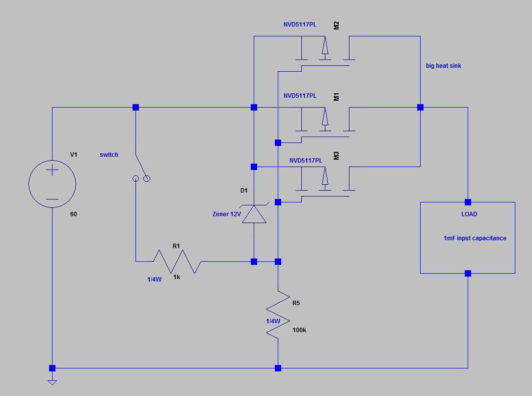
And here is a solution if you have to control the switch from below:
Answer to question 2: There is apparently no problem with your second approach, but we don't know the whole story: is there anything else connected to the battery? we need to know the whole circuitry to answer to this question. Also, you may connect the ground after the mosfet switch, if the battery is floating. Finally, are you sure you know how to connect mosfets in series to distribute the power? this is not as trivial as parallelizing them for a switch!
Note: Again, I would implement 2 or 3 n-mos in parallel, in place of 2 n-mos in series.
It's still unclear what you are really asking, so I'll discuss the tradeoffs between low and high side switching of power to a load.
Low side switching
The main advantage of low side switching is that controlling the switch is easier. This is because the logic that decides whether the switch should be on or off is also generally referenced to the same ground that the switch input is.
For a BJT switch, this can be as easy as a series resistor between a digital output and the base of the BJT. In that case, the emitter would be tied to ground the collector to the low side of the load.
For a "logic level" FET, it can be even easier. The digital output can control the gate directly. The drawback with this is that FETs that can be driven from logic-level voltages have a lower voltage tolerance and lower power handling capability than FETs that require 10-12 V gate drive. However, when the load only draws a few amps and run from 30 V or less, a N channel logical level low side FET switch can be a good choice.
High side switching
The main drawback to high side switching is that you have to provide the gate or base control signal relative to the supply voltage, not relative to the ground where the logic usually is. Another problem is that when using an N channel FET, the gate drive has to exceed the supply voltage by the full gate-on voltage, usually 10-12 V for power FETs.
There are FET gate drivers with level translators and charge pumps built in. The input is a normal ground-reference logic signal, and the output is 0 or 12 V above the positive supply, controlled by the input signal. These FET drivers rely on switching edges to run the charge pump to make the 12 V above the supply, so require regular switching. There is no free lunch.
It is usually easier to use a P channel FET or PNP bipolar transistor for the high side switch. These don't need voltages above the supply to operate. However, P channel FETs usually have slightly worse characteristics than the N channel version with the same gate drive level, voltage tolerance, and current capability. Still, this can be a viable alternative unless the load draws high current where every mΩ of RDSON matters.
A PNP can be particularly easy to drive since you only need to draw some current from the base. If you can tolerate the few 100 mV saturation voltage and the slow turn off, then a PNP is about the easiest solution for a high side switch.
Load requirements
All the preceding was about the controlling the switch and the switch itself. The load may require high or low side switching for its purposes. In fact, this is the main reason to use high side switching at all. When the load is floating, like a motor, solenoid, light bulb, etc, then there is little reason not to use a low side switch.
When the load is connected to ground-referenced signals on its own, then you usually need to use high-side switching. You mentioned CAN and RS-485 connections. If these go to the load being switched, then you pretty much have to switch the high side.
Think of this from the load's point of view. When it is off, everyone else's ground will look like -60 V to the load. It is very unlikely that the CAN or RS-485 interface is designed to go high impedance when the load is off, and can tolerate being held at -60 V at the same time.
for floating loads, low side switching + galvanically isolate communication interface could potentially be used instead of a high side switch?
Yes, that can work. This is assuming when you say "communication interface", you really include all ground-referenced signals connected to the load being switched. There is nothing special about these signals being communication interfaces.
Some communication interfaces are harder to isolate that others. For example, the point to point ethernet varieties are easy since they are already transformer-isolated. You don't need to do anything special to connect a 10-baseT or 100-baseT ethernet to a floating device.
On the other hand, CAN is a lot more tricky. CAN requires sensing the state of the bus with sub-bit timing. For a CAN bus running at 1 MBaud, you don't want delays in writing or reading to exceed around 100 ns (1/10 bit time).

1 comment thread