Thermal relief for through-hole on multi-layer PCB
When using through-hole ("THR") connectors on a multi-layer PCB, I frequently notice problems with the ground pins, when these are connected to the ground plane(s) through various "thermal relief" layouts. When this happens, the reflow soldering job becomes mediocre and hand soldering is nearly impossible.
Example of a bad one I had problems with the other day when hand soldering:

Red=ground plane. It didn't even need to handle this much current, the trace is 1.28mm [0.050inch] wide. This one was impossible to solder well even when we pre-heated the whole PCB.
Whenever I inspect the layouts in the CAD system, they never seem to follow a standard, but various designers seem to make these up as they go, on a case-to-case basis. Cross shapes, star shapes, varied amounts of traces on the stars...
My question: are there any canonical reference designs for how to do thermal relief proper? Or at least some proven in use?
And how do you calculate the maximum current, I'm assuming one just adds the width of all traces?
1 answer
That's a rather strange thermal relief pattern. It's also not clear where the hole is supposed to be.
A proper thermal pattern has a plated hole and annular ring around the hole as usual. Then there is a gap with only a few narrow bridges connecting the annular ring with the surrounding plane. It is common for there to be four bridges, each 90° from the next. The total copper of the bridges is what defines the current capability of the pad and ultimately the connection.
Your picture doesn't show where the hole is. Here is the only interpretation that makes any sense:
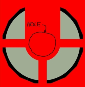
Now we can see that you have a normal thermal pattern, except that the top bridge is much wider than the others. If this top bridge were the same width as the other three, then you probably wouldn't have had any problems with soldering.
So why is the top bridge so wide? You don't say what tool you are using, but you probably have some attribute set for this net that requires a certain minimum trace width. The tool then had to resolve the conflicting requirements of needing to make a pad with thermal relief and needing a minimum trace thickness. What this tool did in this case was apparently to start with a normal thermal pattern, then draw the wide trace over it. The tool designers apparently didn't put a lot of effort into resolving these conflicting requirements from the user.
A better tool might have made each of the bridges ¼ of the required trace width, then grown the whole thermal pattern as necessary to make it still work like a thermal pattern. However, that could cause other problems. Tools "automatically" fixing things can cause lots of trouble.
In the end, you need to resolve this by not providing conflicting requirements. First, decide how much current this pad needs to carry, then use that to decide on the minimum required trace width. Once you have that, set up the thermal pattern so that the four bridges add up to the minimum trace width, and grow its diameter as necessary so that the bridges add up to only a small fraction of the thermally-insulated ring.
If you really need high current capability, then maybe you don't get to use thermals at all, or they'd be so large to make them ineffective. If that is the case, then you need to adjust your manufacturing practices accordingly.

0 comment threads