Comments on MOSFET protection with TVS: at the source pin or at the drain pin
Post
MOSFET protection with TVS: at the source pin or at the drain pin
In the auotmotive context, does it matter where the fat load-dump grade diode is placed in relation to the MOSFET so as to protect it from both fast positive transients and the longer load dump ?
Thank you
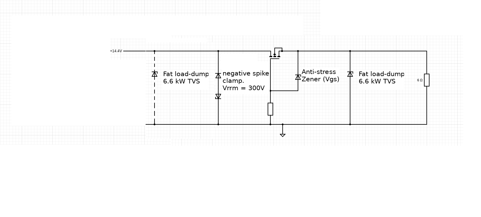
The zener connected in the negative feedback loop regulates the voltage of the load anyway.I dont see the reason for that many zener diodes...
Lundin The ESD TVS is a fast Zener by nature. How would you choose the breakdown voltage of the ESD TVS? It has to protect the MOSFET, so it needs to be upstream of the MOSFET. At the same time, it needs to survive a load dump. The voltage in the load dump pulse is around 90V, which is orders of magnitude lower than in the ESD pulse. But a load dump pulse lasts orders of magnitude longer. ESD TVS are usually fairly small devices. [Are there big ESD TVSes?] I have a nagging suspicion that a typical ESD TVS would be fried by a load dump pulse, if it starts to conduct. So, would you pick the ESD TVS with a breakdown above the load dump voltage, and have a MOSFET rated for a [still] higher voltage?
misk94555 It's more like: you get ESD protection for free. As for protecting the MOSFET I'm no expert but I believe the gate-source voltage is what might damage it and if so the TVS after the MOSFET does that. Of course it helps if the MOSFET is also rugged. I've used a similar polarity protection circuit successfully in industrial applications - although if you want to handle big surges then this might not be enough.
Skipping 1 deleted comment.
Lundin I’m a bit skeptical that a MOSFET drain is sufficiently protected against ESD “for free”. It's true that drain is more resilient against ESD than gate. MOSFETs with higher avalanche ratings are more resilient against ESD to a drain. Nevertheless, I've seen N-channel MOSFETs in an open drain output configuration that got zapped by ESD to the drain. I saw that happen in the field, and I’ve inflicted that with an ESD gun too. After I’ve added a TVS to the open drain output, the ESD fairy stopped going there.
On a different note, the way the P-channel MOSFET is drawn in this schematic doesn’t look right to me. The source should be on the left. [Common schematic error. I draw a P-channel correctly from a third attempt myself.]
misk94555 No, drain should be to the left, that's the whole trick and what the whole design is based on. It is purposely mounted backwards. The body diode should be included in the symbol to make it even clearer though.

This community is part of the non-profit Codidact network. We have other communities too — take a look!
You can also join us in chat!
Want to advertise this community? Use our templates!
Like what we're doing? Support us! Donate
1 comment thread