Post History
To understand why complementary pairs are used, it's probably a good idea to think about the limitations of the NPN emitter-follower circuit: - It's a good circuit for delivering modest powers to ...
#2: Post edited
- To understand why complementary pairs are used, it's probably a good idea to think about the limitations of the NPN emitter-follower circuit: -
- 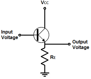
- It's a good circuit for delivering modest powers to a load but its main disadvantage is that it dissipates excessive power in the emitter resistor. Hence, the emitter resistor is replaced by a PNP emitter-follower stage: -
- 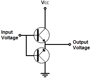
This is a simplified diagram that doesn't show the required biasing arrangement on both bases but, because the PNP transistor is an active device, its ability to pull the output down when required or remain quite high impedance when the loading is light reduces power dissipation considerably.
- To understand why complementary pairs are used, it's probably a good idea to think about the limitations of the NPN emitter-follower circuit: -
- 
- It's a good circuit for delivering modest powers to a load but its main disadvantage is that it dissipates excessive power in the emitter resistor. Hence, the emitter resistor is replaced by a PNP emitter-follower stage: -
- 
- This is a simplified diagram that doesn't show the required biasing arrangement on both bases but, because the PNP transistor is an active device, its ability to pull the output down when required or remain quite high impedance when the loading is light reduces power dissipation considerably.
- The two devices are matched on power, current and voltage ratings. These are the important 1st parameters. Secondary to this is matching the hFE (beta or current gain) of both transistors. Given that most push-pull circuits of this type are used within a regime of negative feedback, some of the more esoteric parameters needn't be so well matched because feedback will compensate most shortcomings.
#1: Initial revision
To understand why complementary pairs are used, it's probably a good idea to think about the limitations of the NPN emitter-follower circuit: -  It's a good circuit for delivering modest powers to a load but its main disadvantage is that it dissipates excessive power in the emitter resistor. Hence, the emitter resistor is replaced by a PNP emitter-follower stage: -  This is a simplified diagram that doesn't show the required biasing arrangement on both bases but, because the PNP transistor is an active device, its ability to pull the output down when required or remain quite high impedance when the loading is light reduces power dissipation considerably.


