Post History
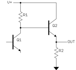
First, let's nail down what circuit you are asking about. Your description is somewhat vague, so I picked this interpretation: Q2 is the emitter follower stage, driven by the previous common emit...
#2: Post edited
- First, let's nail down what circuit you are asking about. Your description is somewhat vague, so I picked this interpretation:
- 
Q2 is the emitter follower stage, driven by the previous common emitter stage of Q1. Your question seems to by why R2 exists.- Some load is needed at DC to pull the emitter of Q2 low when its base is being driven low. R2 is therefore needed whenever the load does not provide this pulldown function. There are various reasons for this. Some are:<ol>
- <li>The load is capacitively coupled.
- <li>The load itself is capacitive or has a substantial capacitive component. R2 and this capacitance form a time constant to bring the output low "fast enough" for whatever the application is.
- <li>The circuit is designed to work with a wide range of loads.
- <li>The circuit must still have a valid output signal even with no load.
- </ol>
- First, let's nail down what circuit you are asking about. Your description is somewhat vague, so I picked this interpretation:
- 
- Q2 is the emitter follower stage, driven by the previous common emitter stage of Q1. Your question seems to be why R2 exists.
- Some load is needed at DC to pull the emitter of Q2 low when its base is being driven low. R2 is therefore needed whenever the load does not provide this pulldown function. There are various reasons for this. Some are:<ol>
- <li>The load is capacitively coupled.
- <li>The load itself is capacitive or has a substantial capacitive component. R2 and this capacitance form a time constant to bring the output low "fast enough" for whatever the application is.
- <li>The circuit is designed to work with a wide range of loads.
- <li>The circuit must still have a valid output signal even with no load.
- </ol>
#1: Initial revision
First, let's nail down what circuit you are asking about. Your description is somewhat vague, so I picked this interpretation:  Q2 is the emitter follower stage, driven by the previous common emitter stage of Q1. Your question seems to by why R2 exists. Some load is needed at DC to pull the emitter of Q2 low when its base is being driven low. R2 is therefore needed whenever the load does not provide this pulldown function. There are various reasons for this. Some are:<ol> <li>The load is capacitively coupled. <li>The load itself is capacitive or has a substantial capacitive component. R2 and this capacitance form a time constant to bring the output low "fast enough" for whatever the application is. <li>The circuit is designed to work with a wide range of loads. <li>The circuit must still have a valid output signal even with no load. </ol>


