Post History
I am eager to create a flyback converter for driving the high side MOSFET. Here is a snapshot of my work so far: 555 timer starts with generating ~100kHz 12V signal on Q1. Q2 is monitoring the v...
#4: Post edited
by
 2kind
·
2020-12-12T16:56:09Z (over 4 years ago)
2kind
·
2020-12-12T16:56:09Z (over 4 years ago)
- I am eager to create a flyback converter for driving the high side MOSFET. Here is a snapshot of my work so far:
- 
- 555 timer starts with generating ~100kHz 12V signal on Q1. Q2 is monitoring the voltage on C2 and when it reaches around 18.7V
- forward biases the OC1 which at the end kills the PWM by tying the RESET pin to the ground.
- MOSFET gate is being controlled through "GATE_CTRL" signal which then turns the OC2 which by the end saturates Q3 and turns the
- Q4 on. Q5 is here to fastly discharge the gate capacitance when "GATE_CTRL" is going off.
- The max. switching frequency is not important here although it should be possible to go up to 30kHz given the MOSFET total gate charge([link](https://www.st.com/resource/en/datasheet/scth100n65g2-7ag.pdf))
- _I would like to use the same circuit idea elsewhere on the board(where for example I need just a flyback converter for driving other circuitry) and wondering how much ripple could I inherently expect across C2?_
- Obviously, driving the Mosfets 100-200mV of ripple on 18.7V across the gate is ok, but what if I want to power other digital circuitry such as CAN transceiver or maybe even the MCU, for example.
- Zener diode is [PDZ18BGWJ](https://assets.nexperia.com/documents/data-sheet/PDZ-GW_SER.pdf), which doesn't have a narrow breakdown region at 25C(if 0.7V across Q2 is added - it should be between 18.3 and 19V which is OK given the purpose shown on the image).
- _Would it make more sense to use an LDO or voltage reference instead of the Zener if precisely 3V3 or 5V(even if ripple is not the issue) is needed in some other use cases?_
- -----
- I will try to answer some questions asked mainly by Olin, but Andy as well.
- > Your circuit makes no sense to me. The nodes POWER IN and POWER OUT cannot be outputs so, where is the load connected?
- As Olin explained, the point of the circuit is to act as an isolated Mosfet gate driver circuit. The positive terminal of the supply would be connected to "POWER_IN" while "POWER_OUT" would be the output to the load.
- > Switching is going to be "slow", due to the opto-isolator, and the fact that the only thing turning off the switch is a pulldown resistor (R6). That may be fine, but don't expect to do PWM at 10s of kHz without a lot of loss.
- I am totally fine with that. Let's assume 18V across Vgs and 3.3nF of gate capacitance(taken from the [datasheet](https://www.st.com/resource/en/datasheet/scth100n65g2-7ag.pdf)). R6 would limit the discharge current to 8mA which would at the end discharge the 3.3nF capacitance in 7us. Since I am not looking for this circuit to be a PWM switching one I am OK on this one.
- > What's with the 18 V? Does your FET really need that much gate drive? I didn't look it up, but most such FETs are rated for 10V and will operate very nicely with 12V. If so, the higher voltage is just slowing down the switch-off time and wasting power.
- Ha! Q4 is SiC and they do allow up to 22V and go even negative -4V to -5V. The higher the Vgs the lower _Rds_on_ would be.
- > 1 mF seems really excessive for the power supply output cap (C2). A lot of capacitance there doesn't do much harm, but that's a lot of space and expense for no apparent gain...
- Let's try to dig in some math. 100kHz of fsw would give 5us of ON time which will end up being 12V/475uH = 25kA/s on the primary of L1(126mA on 5us period). Q1 could easily grasp this without getting hot and it's well within the limits of L1.
- On the secondary side, this would end up being 20.4V/1.3mH=15.7kA/s=80mA. Let's try to see how much capacitance is needed at all to limit the voltage drop on C2 to no more than 50mV when turning the Q4 on.
Q4 datasheet claims 1 ohm of resistance on the gate and since no other resistance is present along with 3.3nF at the gate the rise time would end up being 3.3ns. Very conservatively, even if 5tau is needed for opening the Q4(and it's not because Vgs_th is in a couple of volts range) this is 15ns. Figure the current needed for this is 3.3nF*17.3V/15ns=3A. If we assume "zero resistance" of C2(which we definitely couldn't without being switched to ceramics) the capacitance needed for C2 is 3A*15ns/50mV = 1uF.- Let's increase this to a reasonable 4.7uF and add 2 of them to further decrease the ESR. I haven't checked the math but it should be fine. Electrolytic C2 is then being replaced with 2x4.7uF ceramics which are easy to find on that voltage levels.
- > Do you really need 7.5 mA thru the LED of OC1 just to have its output pull down the reset line against a 10 kΩ pullup? I didn't look up that opto-coupler, but this seems silly.
- I was maybe being too conservative here because I checked the [datasheet ](https://toshiba.semicon-storage.com/info/docget.jsp?did=53135&prodName=TLX9185A)and seen CTR ranging from 20% to 600% in total temperature span.
- I am eager to create a flyback converter for driving the high side MOSFET. Here is a snapshot of my work so far:
- 
- 555 timer starts with generating ~100kHz 12V signal on Q1. Q2 is monitoring the voltage on C2 and when it reaches around 18.7V
- forward biases the OC1 which at the end kills the PWM by tying the RESET pin to the ground.
- MOSFET gate is being controlled through "GATE_CTRL" signal which then turns the OC2 which by the end saturates Q3 and turns the
- Q4 on. Q5 is here to fastly discharge the gate capacitance when "GATE_CTRL" is going off.
- The max. switching frequency is not important here although it should be possible to go up to 30kHz given the MOSFET total gate charge([link](https://www.st.com/resource/en/datasheet/scth100n65g2-7ag.pdf))
- _I would like to use the same circuit idea elsewhere on the board(where for example I need just a flyback converter for driving other circuitry) and wondering how much ripple could I inherently expect across C2?_
- Obviously, driving the Mosfets 100-200mV of ripple on 18.7V across the gate is ok, but what if I want to power other digital circuitry such as CAN transceiver or maybe even the MCU, for example.
- Zener diode is [PDZ18BGWJ](https://assets.nexperia.com/documents/data-sheet/PDZ-GW_SER.pdf), which doesn't have a narrow breakdown region at 25C(if 0.7V across Q2 is added - it should be between 18.3 and 19V which is OK given the purpose shown on the image).
- _Would it make more sense to use an LDO or voltage reference instead of the Zener if precisely 3V3 or 5V(even if ripple is not the issue) is needed in some other use cases?_
- -----
- I will try to answer some questions asked mainly by Olin, but Andy as well.
- > Your circuit makes no sense to me. The nodes POWER IN and POWER OUT cannot be outputs so, where is the load connected?
- As Olin explained, the point of the circuit is to act as an isolated Mosfet gate driver circuit. The positive terminal of the supply would be connected to "POWER_IN" while "POWER_OUT" would be the output to the load.
- > Switching is going to be "slow", due to the opto-isolator, and the fact that the only thing turning off the switch is a pulldown resistor (R6). That may be fine, but don't expect to do PWM at 10s of kHz without a lot of loss.
- I am totally fine with that. Let's assume 18V across Vgs and 3.3nF of gate capacitance(taken from the [datasheet](https://www.st.com/resource/en/datasheet/scth100n65g2-7ag.pdf)). R6 would limit the discharge current to 8mA which would at the end discharge the 3.3nF capacitance in 7us. Since I am not looking for this circuit to be a PWM switching one I am OK on this one.
- > What's with the 18 V? Does your FET really need that much gate drive? I didn't look it up, but most such FETs are rated for 10V and will operate very nicely with 12V. If so, the higher voltage is just slowing down the switch-off time and wasting power.
- Ha! Q4 is SiC and they do allow up to 22V and go even negative -4V to -5V. The higher the Vgs the lower _Rds_on_ would be.
- > 1 mF seems really excessive for the power supply output cap (C2). A lot of capacitance there doesn't do much harm, but that's a lot of space and expense for no apparent gain...
- Let's try to dig in some math. 100kHz of fsw would give 5us of ON time which will end up being 12V/475uH = 25kA/s on the primary of L1(126mA on 5us period). Q1 could easily grasp this without getting hot and it's well within the limits of L1.
- On the secondary side, this would end up being 20.4V/1.3mH=15.7kA/s=80mA. Let's try to see how much capacitance is needed at all to limit the voltage drop on C2 to no more than 50mV when turning the Q4 on.
- Q4 datasheet claims 1 ohm of resistance on the gate and since no other resistance is present along with 3.3nF at the gate the rise time would end up being 3.3ns. Very conservatively, even if 5tau is needed for opening the Q4(and it isn't because Vgs_th is in a couple of volts range) this is 15ns. Figure the current needed for this is 3.3nF*17.3V/15ns=3A. If we assume "zero resistance" of C2(which we definitely couldn't without it being switched to ceramics) the capacitance needed for C2 is 3A*15ns/50mV = 1uF.
- Let's increase this to a reasonable 4.7uF and add 2 of them to further decrease the ESR. I haven't checked the math but it should be fine. Electrolytic C2 is then being replaced with 2x4.7uF ceramics which are easy to find on that voltage levels.
- > Do you really need 7.5 mA thru the LED of OC1 just to have its output pull down the reset line against a 10 kΩ pullup? I didn't look up that opto-coupler, but this seems silly.
- I was maybe being too conservative here because I checked the [datasheet ](https://toshiba.semicon-storage.com/info/docget.jsp?did=53135&prodName=TLX9185A)and seen CTR ranging from 20% to 600% in total temperature span.
#3: Post edited
by
2kind
·
2020-12-12T16:54:10Z (over 4 years ago)
- I am eager to create a flyback converter for driving the high side MOSFET. Here is a snapshot of my work so far:
- 
- 555 timer starts with generating ~100kHz 12V signal on Q1. Q2 is monitoring the voltage on C2 and when it reaches around 18.7V
- forward biases the OC1 which at the end kills the PWM by tying the RESET pin to the ground.
- MOSFET gate is being controlled through "GATE_CTRL" signal which then turns the OC2 which by the end saturates Q3 and turns the
- Q4 on. Q5 is here to fastly discharge the gate capacitance when "GATE_CTRL" is going off.
- The max. switching frequency is not important here although it should be possible to go up to 30kHz given the MOSFET total gate charge([link](https://www.st.com/resource/en/datasheet/scth100n65g2-7ag.pdf))
- _I would like to use the same circuit idea elsewhere on the board(where for example I need just a flyback converter for driving other circuitry) and wondering how much ripple could I inherently expect across C2?_
- Obviously, driving the Mosfets 100-200mV of ripple on 18.7V across the gate is ok, but what if I want to power other digital circuitry such as CAN transceiver or maybe even the MCU, for example.
- Zener diode is [PDZ18BGWJ](https://assets.nexperia.com/documents/data-sheet/PDZ-GW_SER.pdf), which doesn't have a narrow breakdown region at 25C(if 0.7V across Q2 is added - it should be between 18.3 and 19V which is OK given the purpose shown on the image).
- _Would it make more sense to use an LDO or voltage reference instead of the Zener if precisely 3V3 or 5V(even if ripple is not the issue) is needed in some other use cases?_
- -----
- I will try to answer some questions asked mainly by Olin, but Andy as well.
- > Your circuit makes no sense to me. The nodes POWER IN and POWER OUT cannot be outputs so, where is the load connected?
- As Olin explained, the point of the circuit is to act as an isolated Mosfet gate driver circuit. The positive terminal of the supply would be connected to "POWER_IN" while "POWER_OUT" would be the output to the load.
- > Switching is going to be "slow", due to the opto-isolator, and the fact that the only thing turning off the switch is a pulldown resistor (R6). That may be fine, but don't expect to do PWM at 10s of kHz without a lot of loss.
I am totally fine with that. Let's assume 18V across Vgs and 3.3nF of gate capacitance(taken from the [datasheet](https://www.st.com/resource/en/datasheet/scth100n65g2-7ag.pdf)). R6 would limit the discharge current to 8mA which would at the end discharge the 3.3nF capacitance in 7us. Since I am not looking for this circuit to be a switching one I am OK on this one.- > What's with the 18 V? Does your FET really need that much gate drive? I didn't look it up, but most such FETs are rated for 10V and will operate very nicely with 12V. If so, the higher voltage is just slowing down the switch-off time and wasting power.
- Ha! Q4 is SiC and they do allow up to 22V and go even negative -4V to -5V. The higher the Vgs the lower _Rds_on_ would be.
- > 1 mF seems really excessive for the power supply output cap (C2). A lot of capacitance there doesn't do much harm, but that's a lot of space and expense for no apparent gain...
- Let's try to dig in some math. 100kHz of fsw would give 5us of ON time which will end up being 12V/475uH = 25kA/s on the primary of L1(126mA on 5us period). Q1 could easily grasp this without getting hot and it's well within the limits of L1.
- On the secondary side, this would end up being 20.4V/1.3mH=15.7kA/s=80mA. Let's try to see how much capacitance is needed at all to limit the voltage drop on C2 to no more than 50mV when turning the Q4 on.
- Q4 datasheet claims 1 ohm of resistance on the gate and since no other resistance is present along with 3.3nF at the gate the rise time would end up being 3.3ns. Very conservatively, even if 5tau is needed for opening the Q4(and it's not because Vgs_th is in a couple of volts range) this is 15ns. Figure the current needed for this is 3.3nF*17.3V/15ns=3A. If we assume "zero resistance" of C2(which we definitely couldn't without being switched to ceramics) the capacitance needed for C2 is 3A*15ns/50mV = 1uF.
- Let's increase this to a reasonable 4.7uF and add 2 of them to further decrease the ESR. I haven't checked the math but it should be fine. Electrolytic C2 is then being replaced with 2x4.7uF ceramics which are easy to find on that voltage levels.
- > Do you really need 7.5 mA thru the LED of OC1 just to have its output pull down the reset line against a 10 kΩ pullup? I didn't look up that opto-coupler, but this seems silly.
- I was maybe being too conservative here because I checked the [datasheet ](https://toshiba.semicon-storage.com/info/docget.jsp?did=53135&prodName=TLX9185A)and seen CTR ranging from 20% to 600% in total temperature span.
- I am eager to create a flyback converter for driving the high side MOSFET. Here is a snapshot of my work so far:
- 
- 555 timer starts with generating ~100kHz 12V signal on Q1. Q2 is monitoring the voltage on C2 and when it reaches around 18.7V
- forward biases the OC1 which at the end kills the PWM by tying the RESET pin to the ground.
- MOSFET gate is being controlled through "GATE_CTRL" signal which then turns the OC2 which by the end saturates Q3 and turns the
- Q4 on. Q5 is here to fastly discharge the gate capacitance when "GATE_CTRL" is going off.
- The max. switching frequency is not important here although it should be possible to go up to 30kHz given the MOSFET total gate charge([link](https://www.st.com/resource/en/datasheet/scth100n65g2-7ag.pdf))
- _I would like to use the same circuit idea elsewhere on the board(where for example I need just a flyback converter for driving other circuitry) and wondering how much ripple could I inherently expect across C2?_
- Obviously, driving the Mosfets 100-200mV of ripple on 18.7V across the gate is ok, but what if I want to power other digital circuitry such as CAN transceiver or maybe even the MCU, for example.
- Zener diode is [PDZ18BGWJ](https://assets.nexperia.com/documents/data-sheet/PDZ-GW_SER.pdf), which doesn't have a narrow breakdown region at 25C(if 0.7V across Q2 is added - it should be between 18.3 and 19V which is OK given the purpose shown on the image).
- _Would it make more sense to use an LDO or voltage reference instead of the Zener if precisely 3V3 or 5V(even if ripple is not the issue) is needed in some other use cases?_
- -----
- I will try to answer some questions asked mainly by Olin, but Andy as well.
- > Your circuit makes no sense to me. The nodes POWER IN and POWER OUT cannot be outputs so, where is the load connected?
- As Olin explained, the point of the circuit is to act as an isolated Mosfet gate driver circuit. The positive terminal of the supply would be connected to "POWER_IN" while "POWER_OUT" would be the output to the load.
- > Switching is going to be "slow", due to the opto-isolator, and the fact that the only thing turning off the switch is a pulldown resistor (R6). That may be fine, but don't expect to do PWM at 10s of kHz without a lot of loss.
- I am totally fine with that. Let's assume 18V across Vgs and 3.3nF of gate capacitance(taken from the [datasheet](https://www.st.com/resource/en/datasheet/scth100n65g2-7ag.pdf)). R6 would limit the discharge current to 8mA which would at the end discharge the 3.3nF capacitance in 7us. Since I am not looking for this circuit to be a PWM switching one I am OK on this one.
- > What's with the 18 V? Does your FET really need that much gate drive? I didn't look it up, but most such FETs are rated for 10V and will operate very nicely with 12V. If so, the higher voltage is just slowing down the switch-off time and wasting power.
- Ha! Q4 is SiC and they do allow up to 22V and go even negative -4V to -5V. The higher the Vgs the lower _Rds_on_ would be.
- > 1 mF seems really excessive for the power supply output cap (C2). A lot of capacitance there doesn't do much harm, but that's a lot of space and expense for no apparent gain...
- Let's try to dig in some math. 100kHz of fsw would give 5us of ON time which will end up being 12V/475uH = 25kA/s on the primary of L1(126mA on 5us period). Q1 could easily grasp this without getting hot and it's well within the limits of L1.
- On the secondary side, this would end up being 20.4V/1.3mH=15.7kA/s=80mA. Let's try to see how much capacitance is needed at all to limit the voltage drop on C2 to no more than 50mV when turning the Q4 on.
- Q4 datasheet claims 1 ohm of resistance on the gate and since no other resistance is present along with 3.3nF at the gate the rise time would end up being 3.3ns. Very conservatively, even if 5tau is needed for opening the Q4(and it's not because Vgs_th is in a couple of volts range) this is 15ns. Figure the current needed for this is 3.3nF*17.3V/15ns=3A. If we assume "zero resistance" of C2(which we definitely couldn't without being switched to ceramics) the capacitance needed for C2 is 3A*15ns/50mV = 1uF.
- Let's increase this to a reasonable 4.7uF and add 2 of them to further decrease the ESR. I haven't checked the math but it should be fine. Electrolytic C2 is then being replaced with 2x4.7uF ceramics which are easy to find on that voltage levels.
- > Do you really need 7.5 mA thru the LED of OC1 just to have its output pull down the reset line against a 10 kΩ pullup? I didn't look up that opto-coupler, but this seems silly.
- I was maybe being too conservative here because I checked the [datasheet ](https://toshiba.semicon-storage.com/info/docget.jsp?did=53135&prodName=TLX9185A)and seen CTR ranging from 20% to 600% in total temperature span.
#2: Post edited
by
2kind
·
2020-12-12T16:53:01Z (over 4 years ago)
Added answers to comment and answer
- I am eager to create a flyback converter for driving the high side MOSFET. Here is a snapshot of my work so far:
- 
- 555 timer starts with generating ~100kHz 12V signal on Q1. Q2 is monitoring the voltage on C2 and when it reaches around 18.7V
- forward biases the OC1 which at the end kills the PWM by tying the RESET pin to the ground.
- MOSFET gate is being controlled through "GATE_CTRL" signal which then turns the OC2 which by the end saturates Q3 and turns the
- Q4 on. Q5 is here to fastly discharge the gate capacitance when "GATE_CTRL" is going off.
- The max. switching frequency is not important here although it should be possible to go up to 30kHz given the MOSFET total gate charge([link](https://www.st.com/resource/en/datasheet/scth100n65g2-7ag.pdf))
- _I would like to use the same circuit idea elsewhere on the board(where for example I need just a flyback converter for driving other circuitry) and wondering how much ripple could I inherently expect across C2?_
- Obviously, driving the Mosfets 100-200mV of ripple on 18.7V across the gate is ok, but what if I want to power other digital circuitry such as CAN transceiver or maybe even the MCU, for example.
- Zener diode is [PDZ18BGWJ](https://assets.nexperia.com/documents/data-sheet/PDZ-GW_SER.pdf), which doesn't have a narrow breakdown region at 25C(if 0.7V across Q2 is added - it should be between 18.3 and 19V which is OK given the purpose shown on the image).
_Would it make more sense to use an LDO or voltage reference instead of the Zener if precisely 3V3 or 5V(even if ripple is not the issue) is needed in some other use cases?_
- I am eager to create a flyback converter for driving the high side MOSFET. Here is a snapshot of my work so far:
- 
- 555 timer starts with generating ~100kHz 12V signal on Q1. Q2 is monitoring the voltage on C2 and when it reaches around 18.7V
- forward biases the OC1 which at the end kills the PWM by tying the RESET pin to the ground.
- MOSFET gate is being controlled through "GATE_CTRL" signal which then turns the OC2 which by the end saturates Q3 and turns the
- Q4 on. Q5 is here to fastly discharge the gate capacitance when "GATE_CTRL" is going off.
- The max. switching frequency is not important here although it should be possible to go up to 30kHz given the MOSFET total gate charge([link](https://www.st.com/resource/en/datasheet/scth100n65g2-7ag.pdf))
- _I would like to use the same circuit idea elsewhere on the board(where for example I need just a flyback converter for driving other circuitry) and wondering how much ripple could I inherently expect across C2?_
- Obviously, driving the Mosfets 100-200mV of ripple on 18.7V across the gate is ok, but what if I want to power other digital circuitry such as CAN transceiver or maybe even the MCU, for example.
- Zener diode is [PDZ18BGWJ](https://assets.nexperia.com/documents/data-sheet/PDZ-GW_SER.pdf), which doesn't have a narrow breakdown region at 25C(if 0.7V across Q2 is added - it should be between 18.3 and 19V which is OK given the purpose shown on the image).
- _Would it make more sense to use an LDO or voltage reference instead of the Zener if precisely 3V3 or 5V(even if ripple is not the issue) is needed in some other use cases?_
- -----
- I will try to answer some questions asked mainly by Olin, but Andy as well.
- > Your circuit makes no sense to me. The nodes POWER IN and POWER OUT cannot be outputs so, where is the load connected?
- As Olin explained, the point of the circuit is to act as an isolated Mosfet gate driver circuit. The positive terminal of the supply would be connected to "POWER_IN" while "POWER_OUT" would be the output to the load.
- > Switching is going to be "slow", due to the opto-isolator, and the fact that the only thing turning off the switch is a pulldown resistor (R6). That may be fine, but don't expect to do PWM at 10s of kHz without a lot of loss.
- I am totally fine with that. Let's assume 18V across Vgs and 3.3nF of gate capacitance(taken from the [datasheet](https://www.st.com/resource/en/datasheet/scth100n65g2-7ag.pdf)). R6 would limit the discharge current to 8mA which would at the end discharge the 3.3nF capacitance in 7us. Since I am not looking for this circuit to be a switching one I am OK on this one.
- > What's with the 18 V? Does your FET really need that much gate drive? I didn't look it up, but most such FETs are rated for 10V and will operate very nicely with 12V. If so, the higher voltage is just slowing down the switch-off time and wasting power.
- Ha! Q4 is SiC and they do allow up to 22V and go even negative -4V to -5V. The higher the Vgs the lower _Rds_on_ would be.
- > 1 mF seems really excessive for the power supply output cap (C2). A lot of capacitance there doesn't do much harm, but that's a lot of space and expense for no apparent gain...
- Let's try to dig in some math. 100kHz of fsw would give 5us of ON time which will end up being 12V/475uH = 25kA/s on the primary of L1(126mA on 5us period). Q1 could easily grasp this without getting hot and it's well within the limits of L1.
- On the secondary side, this would end up being 20.4V/1.3mH=15.7kA/s=80mA. Let's try to see how much capacitance is needed at all to limit the voltage drop on C2 to no more than 50mV when turning the Q4 on.
- Q4 datasheet claims 1 ohm of resistance on the gate and since no other resistance is present along with 3.3nF at the gate the rise time would end up being 3.3ns. Very conservatively, even if 5tau is needed for opening the Q4(and it's not because Vgs_th is in a couple of volts range) this is 15ns. Figure the current needed for this is 3.3nF*17.3V/15ns=3A. If we assume "zero resistance" of C2(which we definitely couldn't without being switched to ceramics) the capacitance needed for C2 is 3A*15ns/50mV = 1uF.
- Let's increase this to a reasonable 4.7uF and add 2 of them to further decrease the ESR. I haven't checked the math but it should be fine. Electrolytic C2 is then being replaced with 2x4.7uF ceramics which are easy to find on that voltage levels.
- > Do you really need 7.5 mA thru the LED of OC1 just to have its output pull down the reset line against a 10 kΩ pullup? I didn't look up that opto-coupler, but this seems silly.
- I was maybe being too conservative here because I checked the [datasheet ](https://toshiba.semicon-storage.com/info/docget.jsp?did=53135&prodName=TLX9185A)and seen CTR ranging from 20% to 600% in total temperature span.
#1: Initial revision
by
2kind
·
2020-12-11T13:15:00Z (over 4 years ago)
Flyback Converter - Output Ripple
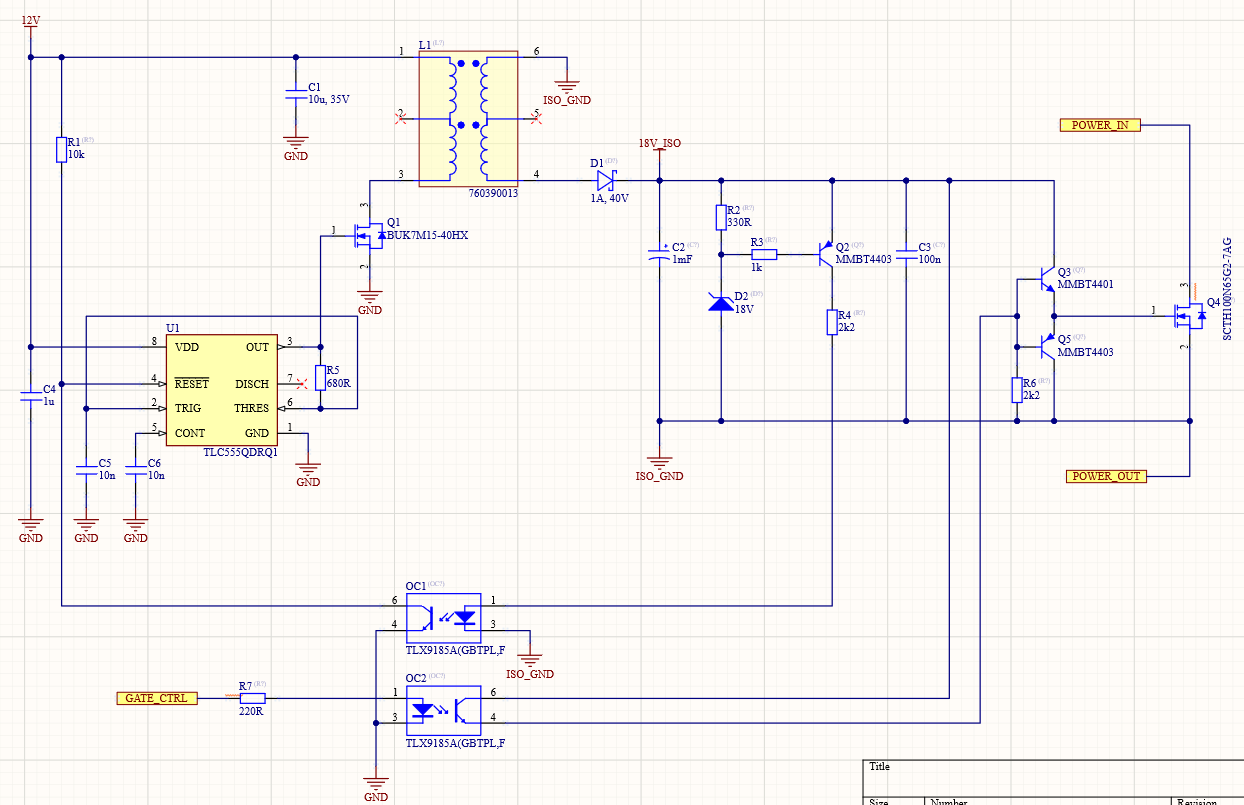
I am eager to create a flyback converter for driving the high side MOSFET. Here is a snapshot of my work so far:  555 timer starts with generating ~100kHz 12V signal on Q1. Q2 is monitoring the voltage on C2 and when it reaches around 18.7V forward biases the OC1 which at the end kills the PWM by tying the RESET pin to the ground. MOSFET gate is being controlled through "GATE_CTRL" signal which then turns the OC2 which by the end saturates Q3 and turns the Q4 on. Q5 is here to fastly discharge the gate capacitance when "GATE_CTRL" is going off. The max. switching frequency is not important here although it should be possible to go up to 30kHz given the MOSFET total gate charge([link](https://www.st.com/resource/en/datasheet/scth100n65g2-7ag.pdf)) _I would like to use the same circuit idea elsewhere on the board(where for example I need just a flyback converter for driving other circuitry) and wondering how much ripple could I inherently expect across C2?_ Obviously, driving the Mosfets 100-200mV of ripple on 18.7V across the gate is ok, but what if I want to power other digital circuitry such as CAN transceiver or maybe even the MCU, for example. Zener diode is [PDZ18BGWJ](https://assets.nexperia.com/documents/data-sheet/PDZ-GW_SER.pdf), which doesn't have a narrow breakdown region at 25C(if 0.7V across Q2 is added - it should be between 18.3 and 19V which is OK given the purpose shown on the image). _Would it make more sense to use an LDO or voltage reference instead of the Zener if precisely 3V3 or 5V(even if ripple is not the issue) is needed in some other use cases?_