Post History
In the circuit below, I am applying a $3.3Vpp$, $63kHz$, 50% Duty Cycle, PWM input signal at the gate of the mosfet and I am expecting to see a similar waveform with different amplitude at the LED...
#1: Initial revision
by
 Georgian
·
2020-12-25T01:46:33Z (over 4 years ago)
Georgian
·
2020-12-25T01:46:33Z (over 4 years ago)
Confused about the amplitude and shape of output voltage pulse
In the circuit below, I am applying a \$3.3Vpp\$, \$63kHz\$, 50% Duty Cycle, PWM input signal at the gate of the mosfet and I am expecting to see a similar waveform with different amplitude at the LED cathode. (I am expecting \$3.3V - V_{F,led}\$ when the Mosfet is ON or \$0V\$ when the mosfet is OFF). According to the datasheet, the typical forward voltage of the LED is \$V_{F}=1.3V\$ for a forward current of around \$I_{F}=10 mA\$.
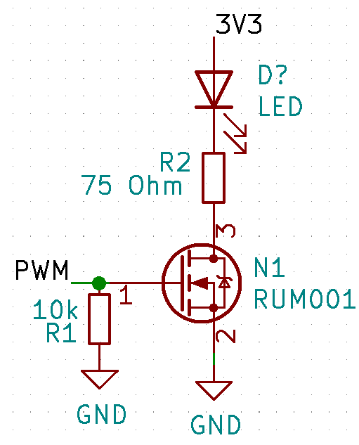
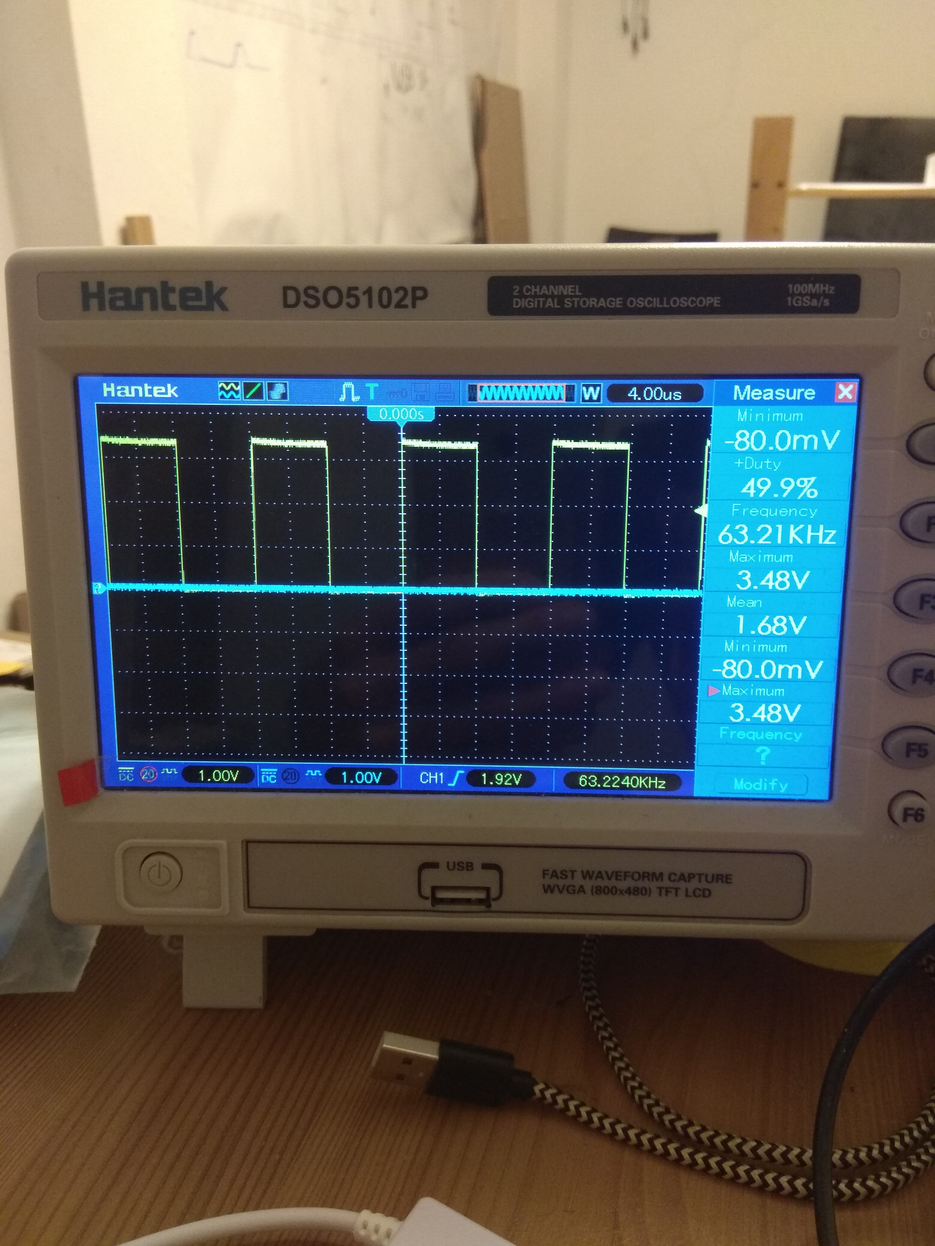
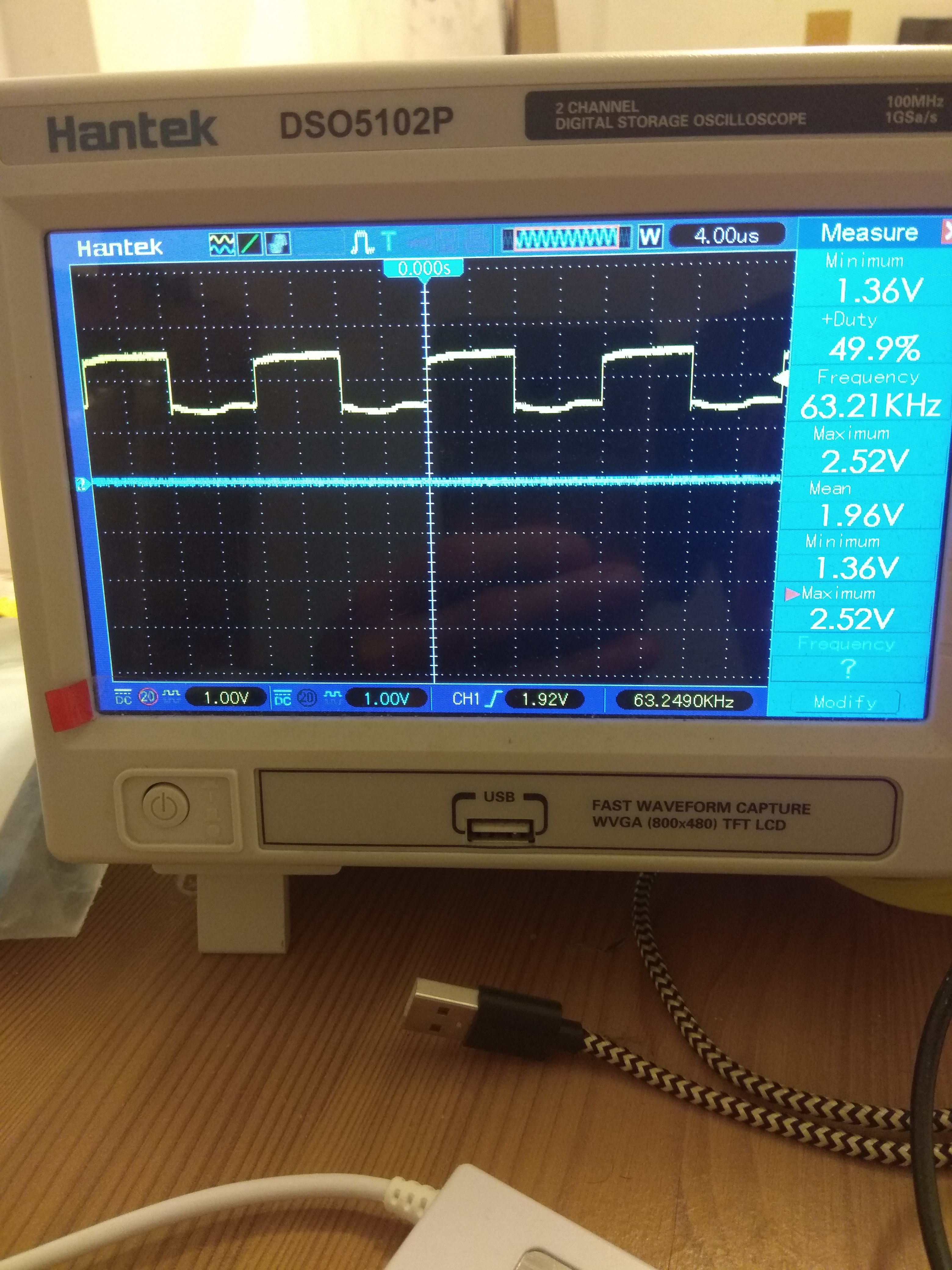
The input PWM signal as well as the voltage at the cathode of the LED (or equally the voltage across resitor \$R2\$ plus the Mosfet's \$R_{DSon}\$) are shown in the two images below as captured from the oscilloscope.
My question is three-fold:
- As you can see, when the input voltage at the gate is at \$3.48 V\$, the voltage at the LED's cathode is at \$2.52 V\$. Why isn't the voltage on the cathode of the LED in this case at \$3.43 - 1.3 \approx 2.1V\$? I.e, where does that extra \$0.5V\$ come from?
- Additionally, why is the \$V_{cathode}\$ at \$1.36V\$ and not \$0V\$ when the PWM input is \$0V\$?
- Lastly, what's the effect that causes \$V_{cathode}\$ to be a bit wavy and not identical in shape with the input PWM pulse?
Thank you and Merry Christmas.