Post History
I'm designing a high side current source that can be controlled with a Digital-to-analog and can source up to 100mA with voltage supply up to 36V. By high side I mean one side of load will be alwa...
#5: Post edited
by
 DeadMouse
·
2022-03-12T14:36:43Z (about 3 years ago)
DeadMouse
·
2022-03-12T14:36:43Z (about 3 years ago)
- I'm designing a high side current source that can be controlled with a Digital-to-analog and can source up to 100mA with voltage supply up to 36V.
- By high side I mean one side of load will be always grounded. Below you can see a reference design of a such circuit.
- 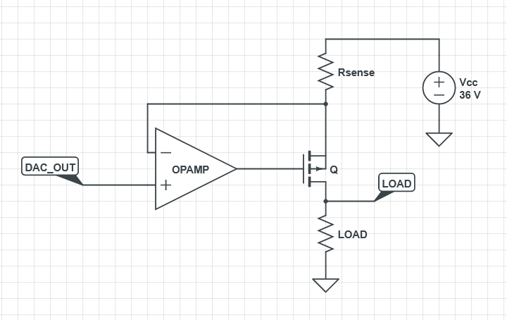
- In the design above the main issue is that the output of the DAC needs extra amplification and also the output of the OP Amp needs to go up to V+ in order to put MOSFET Q to cut-off region.
- Which means the Op Amp needs to have a rail-to-rail output at best and also a wide operating voltage range that can go up to +36V.
- So, I was thinking maybe to do some modifications so I can replace the op amp with something that can work with much lower voltage. Perhaps with the same voltage as DAC works.
- 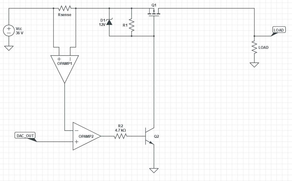
- The OPAMP1 could be a generic differential amplifier or even better an integrated current sense IC that will result in a current to voltage conversion. This will feed the OPAMP2 who can work at the same voltage as the DAC IC.
- When the current goes up, OPAMP1 voltage rises, OPAMP2 pulls its output down to zero, Q2 stops contancting VGS of Q1 decreases and limits the current of the drain-source channel.
- The question:
- I'm very concerned that something will not work regarding the mosfet control circuitry, especially the Q2. Is there something that needs to be done in order to achive smooth control of the current?
- The longer I see the circuit the more confused I get and I'm starting to believe that the gate will start to oscillate.
- Design Specifications:
- * 0.1% accuracy on the output current.
- * Accpetable voltage drop across power elements up to 8V.
- * Lowest voltage across load in zero setpoint must be closest to zero possible.
* Operating voltage range 5V to 36V
- I'm designing a high side current source that can be controlled with a Digital-to-analog and can source up to 100mA with voltage supply up to 36V.
- By high side I mean one side of load will be always grounded. Below you can see a reference design of a such circuit.
- 
- In the design above the main issue is that the output of the DAC needs extra amplification and also the output of the OP Amp needs to go up to V+ in order to put MOSFET Q to cut-off region.
- Which means the Op Amp needs to have a rail-to-rail output at best and also a wide operating voltage range that can go up to +36V.
- So, I was thinking maybe to do some modifications so I can replace the op amp with something that can work with much lower voltage. Perhaps with the same voltage as DAC works.
- 
- The OPAMP1 could be a generic differential amplifier or even better an integrated current sense IC that will result in a current to voltage conversion. This will feed the OPAMP2 who can work at the same voltage as the DAC IC.
- When the current goes up, OPAMP1 voltage rises, OPAMP2 pulls its output down to zero, Q2 stops contancting VGS of Q1 decreases and limits the current of the drain-source channel.
- The question:
- I'm very concerned that something will not work regarding the mosfet control circuitry, especially the Q2. Is there something that needs to be done in order to achive smooth control of the current?
- The longer I see the circuit the more confused I get and I'm starting to believe that the gate will start to oscillate.
- Design Specifications:
- * 0.1% accuracy on the output current.
- * Accpetable voltage drop across power elements up to 8V.
- * Lowest voltage across load in zero setpoint must be closest to zero possible.
- * Operating voltage range 12V to 36V
#4: Post edited
by
DeadMouse
·
2022-03-12T14:36:11Z (about 3 years ago)
- I'm designing a high side current source that can be controlled with a Digital-to-analog and can source up to 100mA with voltage supply up to 36V.
- By high side I mean one side of load will be always grounded. Below you can see a reference design of a such circuit.
- 
- In the design above the main issue is that the output of the DAC needs extra amplification and also the output of the OP Amp needs to go up to V+ in order to put MOSFET Q to cut-off region.
- Which means the Op Amp needs to have a rail-to-rail output at best and also a wide operating voltage range that can go up to +36V.
- So, I was thinking maybe to do some modifications so I can replace the op amp with something that can work with much lower voltage. Perhaps with the same voltage as DAC works.
- 
- The OPAMP1 could be a generic differential amplifier or even better an integrated current sense IC that will result in a current to voltage conversion. This will feed the OPAMP2 who can work at the same voltage as the DAC IC.
- When the current goes up, OPAMP1 voltage rises, OPAMP2 pulls its output down to zero, Q2 stops contancting VGS of Q1 decreases and limits the current of the drain-source channel.
- The question:
- I'm very concerned that something will not work regarding the mosfet control circuitry, especially the Q2. Is there something that needs to be done in order to achive smooth control of the current?
- The longer I see the circuit the more confused I get and I'm starting to believe that the gate will start to oscillate.
- Design Specifications:
- * 0.1% accuracy on the output current.
- * Accpetable voltage drop across power elements up to 8V.
* Lowest voltage across load in zero setpoint must be closest to zero possible.
- I'm designing a high side current source that can be controlled with a Digital-to-analog and can source up to 100mA with voltage supply up to 36V.
- By high side I mean one side of load will be always grounded. Below you can see a reference design of a such circuit.
- 
- In the design above the main issue is that the output of the DAC needs extra amplification and also the output of the OP Amp needs to go up to V+ in order to put MOSFET Q to cut-off region.
- Which means the Op Amp needs to have a rail-to-rail output at best and also a wide operating voltage range that can go up to +36V.
- So, I was thinking maybe to do some modifications so I can replace the op amp with something that can work with much lower voltage. Perhaps with the same voltage as DAC works.
- 
- The OPAMP1 could be a generic differential amplifier or even better an integrated current sense IC that will result in a current to voltage conversion. This will feed the OPAMP2 who can work at the same voltage as the DAC IC.
- When the current goes up, OPAMP1 voltage rises, OPAMP2 pulls its output down to zero, Q2 stops contancting VGS of Q1 decreases and limits the current of the drain-source channel.
- The question:
- I'm very concerned that something will not work regarding the mosfet control circuitry, especially the Q2. Is there something that needs to be done in order to achive smooth control of the current?
- The longer I see the circuit the more confused I get and I'm starting to believe that the gate will start to oscillate.
- Design Specifications:
- * 0.1% accuracy on the output current.
- * Accpetable voltage drop across power elements up to 8V.
- * Lowest voltage across load in zero setpoint must be closest to zero possible.
- * Operating voltage range 5V to 36V
#3: Post edited
by
DeadMouse
·
2022-03-12T14:34:59Z (about 3 years ago)
- I'm designing a high side current source that can be controlled with a Digital-to-analog and can source up to 100mA with voltage supply up to 36V.
- By high side I mean one side of load will be always grounded. Below you can see a reference design of a such circuit.
- 
- In the design above the main issue is that the output of the DAC needs extra amplification and also the output of the OP Amp needs to go up to V+ in order to put MOSFET Q to cut-off region.
- Which means the Op Amp needs to have a rail-to-rail output at best and also a wide operating voltage range that can go up to +36V.
- So, I was thinking maybe to do some modifications so I can replace the op amp with something that can work with much lower voltage. Perhaps with the same voltage as DAC works.
- 
- The OPAMP1 could be a generic differential amplifier or even better an integrated current sense IC that will result in a current to voltage conversion. This will feed the OPAMP2 who can work at the same voltage as the DAC IC.
- When the current goes up, OPAMP1 voltage rises, OPAMP2 pulls its output down to zero, Q2 stops contancting VGS of Q1 decreases and limits the current of the drain-source channel.
- The question:
- I'm very concerned that something will not work regarding the mosfet control circuitry, especially the Q2. Is there something that needs to be done in order to achive smooth control of the current?
- The longer I see the circuit the more confused I get and I'm starting to believe that the gate will start to oscillate.
- Design Specifications:
- * 0.1% accuracy on the output current.
- * Accpetable voltage drop across power elements up to 8V.
* Lowest voltage across load must be closest to zero possible.
- I'm designing a high side current source that can be controlled with a Digital-to-analog and can source up to 100mA with voltage supply up to 36V.
- By high side I mean one side of load will be always grounded. Below you can see a reference design of a such circuit.
- 
- In the design above the main issue is that the output of the DAC needs extra amplification and also the output of the OP Amp needs to go up to V+ in order to put MOSFET Q to cut-off region.
- Which means the Op Amp needs to have a rail-to-rail output at best and also a wide operating voltage range that can go up to +36V.
- So, I was thinking maybe to do some modifications so I can replace the op amp with something that can work with much lower voltage. Perhaps with the same voltage as DAC works.
- 
- The OPAMP1 could be a generic differential amplifier or even better an integrated current sense IC that will result in a current to voltage conversion. This will feed the OPAMP2 who can work at the same voltage as the DAC IC.
- When the current goes up, OPAMP1 voltage rises, OPAMP2 pulls its output down to zero, Q2 stops contancting VGS of Q1 decreases and limits the current of the drain-source channel.
- The question:
- I'm very concerned that something will not work regarding the mosfet control circuitry, especially the Q2. Is there something that needs to be done in order to achive smooth control of the current?
- The longer I see the circuit the more confused I get and I'm starting to believe that the gate will start to oscillate.
- Design Specifications:
- * 0.1% accuracy on the output current.
- * Accpetable voltage drop across power elements up to 8V.
- * Lowest voltage across load in zero setpoint must be closest to zero possible.
#2: Post edited
by
DeadMouse
·
2022-03-12T14:33:44Z (about 3 years ago)
Added design requirements
- I'm designing a high side current source that can be controlled with a Digital-to-analog and can source up to 100mA with voltage supply up to 36V.
- By high side I mean one side of load will be always grounded. Below you can see a reference design of a such circuit.
- 
- In the design above the main issue is that the output of the DAC needs extra amplification and also the output of the OP Amp needs to go up to V+ in order to put MOSFET Q to cut-off region.
- Which means the Op Amp needs to have a rail-to-rail output at best and also a wide operating voltage range that can go up to +36V.
- So, I was thinking maybe to do some modifications so I can replace the op amp with something that can work with much lower voltage. Perhaps with the same voltage as DAC works.
- 
- The OPAMP1 could be a generic differential amplifier or even better an integrated current sense IC that will result in a current to voltage conversion. This will feed the OPAMP2 who can work at the same voltage as the DAC IC.
- When the current goes up, OPAMP1 voltage rises, OPAMP2 pulls its output down to zero, Q2 stops contancting VGS of Q1 decreases and limits the current of the drain-source channel.
- The question:
- I'm very concerned that something will not work regarding the mosfet control circuitry, especially the Q2. Is there something that needs to be done in order to achive smooth control of the current?
The longer I see the circuit the more confused I get and I'm starting to believe that the gate will start to oscillate.
- I'm designing a high side current source that can be controlled with a Digital-to-analog and can source up to 100mA with voltage supply up to 36V.
- By high side I mean one side of load will be always grounded. Below you can see a reference design of a such circuit.
- 
- In the design above the main issue is that the output of the DAC needs extra amplification and also the output of the OP Amp needs to go up to V+ in order to put MOSFET Q to cut-off region.
- Which means the Op Amp needs to have a rail-to-rail output at best and also a wide operating voltage range that can go up to +36V.
- So, I was thinking maybe to do some modifications so I can replace the op amp with something that can work with much lower voltage. Perhaps with the same voltage as DAC works.
- 
- The OPAMP1 could be a generic differential amplifier or even better an integrated current sense IC that will result in a current to voltage conversion. This will feed the OPAMP2 who can work at the same voltage as the DAC IC.
- When the current goes up, OPAMP1 voltage rises, OPAMP2 pulls its output down to zero, Q2 stops contancting VGS of Q1 decreases and limits the current of the drain-source channel.
- The question:
- I'm very concerned that something will not work regarding the mosfet control circuitry, especially the Q2. Is there something that needs to be done in order to achive smooth control of the current?
- The longer I see the circuit the more confused I get and I'm starting to believe that the gate will start to oscillate.
- Design Specifications:
- * 0.1% accuracy on the output current.
- * Accpetable voltage drop across power elements up to 8V.
- * Lowest voltage across load must be closest to zero possible.
#1: Initial revision
by
DeadMouse
·
2022-03-12T13:06:13Z (about 3 years ago)
DAC controlled high side current source.
I'm designing a high side current source that can be controlled with a Digital-to-analog and can source up to 100mA with voltage supply up to 36V. By high side I mean one side of load will be always grounded. Below you can see a reference design of a such circuit.  In the design above the main issue is that the output of the DAC needs extra amplification and also the output of the OP Amp needs to go up to V+ in order to put MOSFET Q to cut-off region. Which means the Op Amp needs to have a rail-to-rail output at best and also a wide operating voltage range that can go up to +36V. So, I was thinking maybe to do some modifications so I can replace the op amp with something that can work with much lower voltage. Perhaps with the same voltage as DAC works.  The OPAMP1 could be a generic differential amplifier or even better an integrated current sense IC that will result in a current to voltage conversion. This will feed the OPAMP2 who can work at the same voltage as the DAC IC. When the current goes up, OPAMP1 voltage rises, OPAMP2 pulls its output down to zero, Q2 stops contancting VGS of Q1 decreases and limits the current of the drain-source channel. The question: I'm very concerned that something will not work regarding the mosfet control circuitry, especially the Q2. Is there something that needs to be done in order to achive smooth control of the current? The longer I see the circuit the more confused I get and I'm starting to believe that the gate will start to oscillate.