Post History
Building on a previous question about terminology, I am trying to arrive at a solution to connect a digital air pressure regulator that sinks current as part of its 4-20 mA current feedback loop to...
#4: Post edited
by
 JYelton
·
2023-04-08T16:44:56Z (about 2 years ago)
JYelton
·
2023-04-08T16:44:56Z (about 2 years ago)
Added block diagram
- Building on [a previous question about terminology](https://electrical.codidact.com/posts/288027), I am trying to arrive at a solution to connect a digital air pressure regulator that sinks current as part of its 4-20 mA current feedback loop to an ADC that _also_ sinks current.
- The pressure regulator has two 4-20 mA loops, and sinks current for both of them. The control loop (sets the desired pressure) is handled by an [Analog Devices AD74413R](https://www.analog.com/en/products/ad74413r.html) ([Datasheet](https://www.analog.com/media/en/technical-documentation/data-sheets/AD74413R.pdf)) and is working without a problem. The feedback loop (reports actual pressure) is intended to be handled by an [Analog Devices AD4111](https://www.analog.com/en/products/ad4111.html) ([Datasheet](https://www.analog.com/media/en/technical-documentation/data-sheets/ad4111.pdf)), but since both endpoints sink current, I need to create a bridge or adapter circuit.
- A colleague and I used this [TI Application Note](https://www.ti.com/lit/an/slaa866/slaa866.pdf) as the basis for the following schematics:
- **Schematic 1:**<br />
- 
- **Schematic 2:** _(connects at right of schematic 1)_<br/>
- 
- We first created [a simulation in Falstad](https://falstad.com/circuit/circuitjs.html?ctz=CQAgjCAMB0l3BWcMBMcUHYMGZIA4UA2ATmIxABY8QkFIaBTAWjDACgAncBBFZFCuEJ56YSAKggUBOJyEj+gsMNEplkitjRywxXuDWFwevqzSSi0DGwDu81et36whqGwAuxyEu+iTyCnpRECZsaDwRFGJCEkIMBGIiFGwoaEIECgwKYkgsQIxiCkzkegATBgAzAEMAVwAbdx1-MQQjJ1N8anptO3bFY30yI0hbAb4hqTAMIwmR3owXfuUFMQk58AWOiSnp-vWpovAXUSyfVrd5w5a2rDbIc5Gqjd2xQPA8DA634hpJMXg4KkiAg8LhsIRINgCrdyKh0nhlDwsi4RMQIP94KM+mY-M5Om4oaIPl8-N4AsEgljmsd3tsafsCEoaQcmeYRoSpJBHK41C9XBBKVwXFQjuZhdRZpzHuAiqJxEoeFtBD8kHKAd1oHR4Nk8KQ0EkpJqSpihYrRaJZea-uq2AAjEBo5UoUxgbBKN0Cu2ciSJJDOjLgN2wtgAD29yrA1DUuQdakoUkEAEEACIUVjsMNopBolLp8bqQQSAAKHAYAGcyzVSwAdMulgDm9Sq7gA9hwvawEORErnSKI3SkRmHOz9HdxzGjyIXBABhKulgB27iY5QADgwF+Ul7WAMbzjfuWtlltVncMNgAJUmuwmvLubyClHoqskMAQbHr17aPKm38IgkpT9rgMRx7j-AC3CvcUHReSNlV2R83hfIJNSxARqBxI5hCtfZlitVgyUw-ZLX+DDLVmLESN8GU3jET43CFcF6AmaDJQxWQhXQ-CmJw41ZF6EjmSo+j9jNTCwDE+ULho5iXh4ijeh48TBLZHQlOo10IRg4Y+JGID1No9SRLcABLI5COZMDeJgLksSs8T7NcdY0G5RxmicthsGoTQQAAMQFVI4AA2AUCQFgQDnDhF0aIA).
- We have been struggling because our knowledge of opamps is a bit rusty/weak. I will explain the thinking, as well as what is happening. This circuit has been built on a prototype PCB. Initial tests indicated it would work, but connecting it to the AD4111 yielded different results.
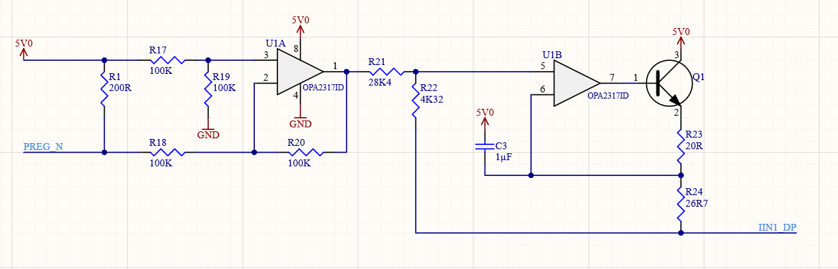
- `PREG_N` connects to the pressure regulator. The amount of current it sinks to effectively report pressure is measured by the voltage drop across R1. The right half of schematic 1 is based on the TI application note and is a voltage-to-current converter. The left half of schematic 1 is a current-to-voltage converter which was using the opamp as a differential amplifier with unity gain. `IIN_DP` connects to a current input channel of the AD4111.
- The ratio between the two voltage dividers (R21-22, R23-24) determines how much current is driven based on the input voltage.
- We failed to include the load resistance in the simulation, however. There is 50 Ω load resistance internal to the AD4111, and an additional 180 Ω in series which was used based on the AD4111 evaluation board. With a 5 V source, there can only be a maximum of 250 Ω resistance and still allow 20 mA.
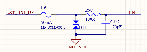
- In troubleshooting the physical circuit, we replaced the fuse and 180 Ω resistor with 0 Ω jumpers and removed the TVS diode and capacitor to eliminate variables.
- If a 50 Ω load resistor is added in the simulation, we see the same as what we observe with the physical circuit: that for a 10 mA input current, only 8 mA is driven at the output.
- Changing the 26.7 Ω resistor to 20 Ω resolves this issue and appears to work for the full range of 4 to 20 mA input in simulation. However, it then becomes dependent on the load resistance, which will vary between devices, and defeats the purpose of the current source.
- I'm starting to feel that this solution is the wrong approach. I've tested a variety of different component values in simulation but output current always varies by load resistance.
- I'd prefer to tweak this design since we already have some PCBs that use the schematic, but if a completely new circuit is warranted, I'm open to suggestions on what to use. I've been researching current mirrors and current sources, but I don't really know if those are the hammer for this nail.
- Can I modify this circuit to get the desired result or should I scrap it and start over?[]()
- Building on [a previous question about terminology](https://electrical.codidact.com/posts/288027), I am trying to arrive at a solution to connect a digital air pressure regulator that sinks current as part of its 4-20 mA current feedback loop to an ADC that _also_ sinks current.
- **Block Diagram:**
- 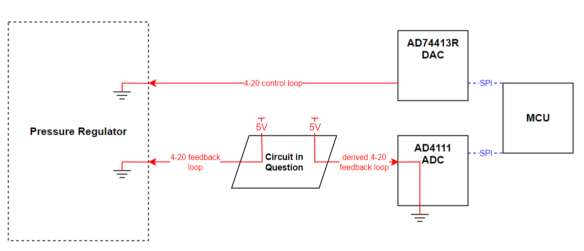
- The pressure regulator has two 4-20 mA loops, and sinks current for both of them. The control loop (sets the desired pressure) is handled by an [Analog Devices AD74413R](https://www.analog.com/en/products/ad74413r.html) ([Datasheet](https://www.analog.com/media/en/technical-documentation/data-sheets/AD74413R.pdf)) and is working without a problem. The feedback loop (reports actual pressure) is intended to be handled by an [Analog Devices AD4111](https://www.analog.com/en/products/ad4111.html) ([Datasheet](https://www.analog.com/media/en/technical-documentation/data-sheets/ad4111.pdf)), but since both endpoints sink current, I need to create a bridge or adapter circuit.
- A colleague and I used this [TI Application Note](https://www.ti.com/lit/an/slaa866/slaa866.pdf) as the basis for the following schematics:
- **Schematic 1:**<br />
- 
- **Schematic 2:** _(connects at right of schematic 1)_<br/>
- 
- We first created [a simulation in Falstad](https://falstad.com/circuit/circuitjs.html?ctz=CQAgjCAMB0l3BWcMBMcUHYMGZIA4UA2ATmIxABY8QkFIaBTAWjDACgAncBBFZFCuEJ56YSAKggUBOJyEj+gsMNEplkitjRywxXuDWFwevqzSSi0DGwDu81et36whqGwAuxyEu+iTyCnpRECZsaDwRFGJCEkIMBGIiFGwoaEIECgwKYkgsQIxiCkzkegATBgAzAEMAVwAbdx1-MQQjJ1N8anptO3bFY30yI0hbAb4hqTAMIwmR3owXfuUFMQk58AWOiSnp-vWpovAXUSyfVrd5w5a2rDbIc5Gqjd2xQPA8DA634hpJMXg4KkiAg8LhsIRINgCrdyKh0nhlDwsi4RMQIP94KM+mY-M5Om4oaIPl8-N4AsEgljmsd3tsafsCEoaQcmeYRoSpJBHK41C9XBBKVwXFQjuZhdRZpzHuAiqJxEoeFtBD8kHKAd1oHR4Nk8KQ0EkpJqSpihYrRaJZea-uq2AAjEBo5UoUxgbBKN0Cu2ciSJJDOjLgN2wtgAD29yrA1DUuQdakoUkEAEEACIUVjsMNopBolLp8bqQQSAAKHAYAGcyzVSwAdMulgDm9Sq7gA9hwvawEORErnSKI3SkRmHOz9HdxzGjyIXBABhKulgB27iY5QADgwF+Ul7WAMbzjfuWtlltVncMNgAJUmuwmvLubyClHoqskMAQbHr17aPKm38IgkpT9rgMRx7j-AC3CvcUHReSNlV2R83hfIJNSxARqBxI5hCtfZlitVgyUw-ZLX+DDLVmLESN8GU3jET43CFcF6AmaDJQxWQhXQ-CmJw41ZF6EjmSo+j9jNTCwDE+ULho5iXh4ijeh48TBLZHQlOo10IRg4Y+JGID1No9SRLcABLI5COZMDeJgLksSs8T7NcdY0G5RxmicthsGoTQQAAMQFVI4AA2AUCQFgQDnDhF0aIA).
- We have been struggling because our knowledge of opamps is a bit rusty/weak. I will explain the thinking, as well as what is happening. This circuit has been built on a prototype PCB. Initial tests indicated it would work, but connecting it to the AD4111 yielded different results.
- `PREG_N` connects to the pressure regulator. The amount of current it sinks to effectively report pressure is measured by the voltage drop across R1. The right half of schematic 1 is based on the TI application note and is a voltage-to-current converter. The left half of schematic 1 is a current-to-voltage converter which was using the opamp as a differential amplifier with unity gain. `IIN_DP` connects to a current input channel of the AD4111.
- The ratio between the two voltage dividers (R21-22, R23-24) determines how much current is driven based on the input voltage.
- We failed to include the load resistance in the simulation, however. There is 50 Ω load resistance internal to the AD4111, and an additional 180 Ω in series which was used based on the AD4111 evaluation board. With a 5 V source, there can only be a maximum of 250 Ω resistance and still allow 20 mA.
- In troubleshooting the physical circuit, we replaced the fuse and 180 Ω resistor with 0 Ω jumpers and removed the TVS diode and capacitor to eliminate variables.
- If a 50 Ω load resistor is added in the simulation, we see the same as what we observe with the physical circuit: that for a 10 mA input current, only 8 mA is driven at the output.
- Changing the 26.7 Ω resistor to 20 Ω resolves this issue and appears to work for the full range of 4 to 20 mA input in simulation. However, it then becomes dependent on the load resistance, which will vary between devices, and defeats the purpose of the current source.
- I'm starting to feel that this solution is the wrong approach. I've tested a variety of different component values in simulation but output current always varies by load resistance.
- I'd prefer to tweak this design since we already have some PCBs that use the schematic, but if a completely new circuit is warranted, I'm open to suggestions on what to use. I've been researching current mirrors and current sources, but I don't really know if those are the hammer for this nail.
- Can I modify this circuit to get the desired result or should I scrap it and start over?[]()
#3: Post edited
by
JYelton
·
2023-04-08T16:19:40Z (about 2 years ago)
Added direct links to datasheets
- Building on [a previous question about terminology](https://electrical.codidact.com/posts/288027), I am trying to arrive at a solution to connect a digital air pressure regulator that sinks current as part of its 4-20 mA current feedback loop to an ADC that _also_ sinks current.
The pressure regulator has two 4-20 mA loops, and sinks current for both of them. The control loop (sets the desired pressure) is handled by an [Analog Devices AD74413R](https://www.analog.com/en/products/ad74413r.html) and is working without a problem. The feedback loop (reports actual pressure) is intended to be handled by an [Analog Devices AD4111](https://www.analog.com/en/products/ad4111.html), but since both endpoints sink current, I need to create a bridge or adapter circuit.- A colleague and I used this [TI Application Note](https://www.ti.com/lit/an/slaa866/slaa866.pdf) as the basis for the following schematics:
- **Schematic 1:**<br />
- 
- **Schematic 2:** _(connects at right of schematic 1)_<br/>
- 
- We first created [a simulation in Falstad](https://falstad.com/circuit/circuitjs.html?ctz=CQAgjCAMB0l3BWcMBMcUHYMGZIA4UA2ATmIxABY8QkFIaBTAWjDACgAncBBFZFCuEJ56YSAKggUBOJyEj+gsMNEplkitjRywxXuDWFwevqzSSi0DGwDu81et36whqGwAuxyEu+iTyCnpRECZsaDwRFGJCEkIMBGIiFGwoaEIECgwKYkgsQIxiCkzkegATBgAzAEMAVwAbdx1-MQQjJ1N8anptO3bFY30yI0hbAb4hqTAMIwmR3owXfuUFMQk58AWOiSnp-vWpovAXUSyfVrd5w5a2rDbIc5Gqjd2xQPA8DA634hpJMXg4KkiAg8LhsIRINgCrdyKh0nhlDwsi4RMQIP94KM+mY-M5Om4oaIPl8-N4AsEgljmsd3tsafsCEoaQcmeYRoSpJBHK41C9XBBKVwXFQjuZhdRZpzHuAiqJxEoeFtBD8kHKAd1oHR4Nk8KQ0EkpJqSpihYrRaJZea-uq2AAjEBo5UoUxgbBKN0Cu2ciSJJDOjLgN2wtgAD29yrA1DUuQdakoUkEAEEACIUVjsMNopBolLp8bqQQSAAKHAYAGcyzVSwAdMulgDm9Sq7gA9hwvawEORErnSKI3SkRmHOz9HdxzGjyIXBABhKulgB27iY5QADgwF+Ul7WAMbzjfuWtlltVncMNgAJUmuwmvLubyClHoqskMAQbHr17aPKm38IgkpT9rgMRx7j-AC3CvcUHReSNlV2R83hfIJNSxARqBxI5hCtfZlitVgyUw-ZLX+DDLVmLESN8GU3jET43CFcF6AmaDJQxWQhXQ-CmJw41ZF6EjmSo+j9jNTCwDE+ULho5iXh4ijeh48TBLZHQlOo10IRg4Y+JGID1No9SRLcABLI5COZMDeJgLksSs8T7NcdY0G5RxmicthsGoTQQAAMQFVI4AA2AUCQFgQDnDhF0aIA).
- We have been struggling because our knowledge of opamps is a bit rusty/weak. I will explain the thinking, as well as what is happening. This circuit has been built on a prototype PCB. Initial tests indicated it would work, but connecting it to the AD4111 yielded different results.
- `PREG_N` connects to the pressure regulator. The amount of current it sinks to effectively report pressure is measured by the voltage drop across R1. The right half of schematic 1 is based on the TI application note and is a voltage-to-current converter. The left half of schematic 1 is a current-to-voltage converter which was using the opamp as a differential amplifier with unity gain. `IIN_DP` connects to a current input channel of the AD4111.
- The ratio between the two voltage dividers (R21-22, R23-24) determines how much current is driven based on the input voltage.
- We failed to include the load resistance in the simulation, however. There is 50 Ω load resistance internal to the AD4111, and an additional 180 Ω in series which was used based on the AD4111 evaluation board. With a 5 V source, there can only be a maximum of 250 Ω resistance and still allow 20 mA.
- In troubleshooting the physical circuit, we replaced the fuse and 180 Ω resistor with 0 Ω jumpers and removed the TVS diode and capacitor to eliminate variables.
- If a 50 Ω load resistor is added in the simulation, we see the same as what we observe with the physical circuit: that for a 10 mA input current, only 8 mA is driven at the output.
- Changing the 26.7 Ω resistor to 20 Ω resolves this issue and appears to work for the full range of 4 to 20 mA input in simulation. However, it then becomes dependent on the load resistance, which will vary between devices, and defeats the purpose of the current source.
- I'm starting to feel that this solution is the wrong approach. I've tested a variety of different component values in simulation but output current always varies by load resistance.
- I'd prefer to tweak this design since we already have some PCBs that use the schematic, but if a completely new circuit is warranted, I'm open to suggestions on what to use. I've been researching current mirrors and current sources, but I don't really know if those are the hammer for this nail.
Can I modify this circuit to get the desired result or should I scrap it and start over?
- Building on [a previous question about terminology](https://electrical.codidact.com/posts/288027), I am trying to arrive at a solution to connect a digital air pressure regulator that sinks current as part of its 4-20 mA current feedback loop to an ADC that _also_ sinks current.
- The pressure regulator has two 4-20 mA loops, and sinks current for both of them. The control loop (sets the desired pressure) is handled by an [Analog Devices AD74413R](https://www.analog.com/en/products/ad74413r.html) ([Datasheet](https://www.analog.com/media/en/technical-documentation/data-sheets/AD74413R.pdf)) and is working without a problem. The feedback loop (reports actual pressure) is intended to be handled by an [Analog Devices AD4111](https://www.analog.com/en/products/ad4111.html) ([Datasheet](https://www.analog.com/media/en/technical-documentation/data-sheets/ad4111.pdf)), but since both endpoints sink current, I need to create a bridge or adapter circuit.
- A colleague and I used this [TI Application Note](https://www.ti.com/lit/an/slaa866/slaa866.pdf) as the basis for the following schematics:
- **Schematic 1:**<br />
- 
- **Schematic 2:** _(connects at right of schematic 1)_<br/>
- 
- We first created [a simulation in Falstad](https://falstad.com/circuit/circuitjs.html?ctz=CQAgjCAMB0l3BWcMBMcUHYMGZIA4UA2ATmIxABY8QkFIaBTAWjDACgAncBBFZFCuEJ56YSAKggUBOJyEj+gsMNEplkitjRywxXuDWFwevqzSSi0DGwDu81et36whqGwAuxyEu+iTyCnpRECZsaDwRFGJCEkIMBGIiFGwoaEIECgwKYkgsQIxiCkzkegATBgAzAEMAVwAbdx1-MQQjJ1N8anptO3bFY30yI0hbAb4hqTAMIwmR3owXfuUFMQk58AWOiSnp-vWpovAXUSyfVrd5w5a2rDbIc5Gqjd2xQPA8DA634hpJMXg4KkiAg8LhsIRINgCrdyKh0nhlDwsi4RMQIP94KM+mY-M5Om4oaIPl8-N4AsEgljmsd3tsafsCEoaQcmeYRoSpJBHK41C9XBBKVwXFQjuZhdRZpzHuAiqJxEoeFtBD8kHKAd1oHR4Nk8KQ0EkpJqSpihYrRaJZea-uq2AAjEBo5UoUxgbBKN0Cu2ciSJJDOjLgN2wtgAD29yrA1DUuQdakoUkEAEEACIUVjsMNopBolLp8bqQQSAAKHAYAGcyzVSwAdMulgDm9Sq7gA9hwvawEORErnSKI3SkRmHOz9HdxzGjyIXBABhKulgB27iY5QADgwF+Ul7WAMbzjfuWtlltVncMNgAJUmuwmvLubyClHoqskMAQbHr17aPKm38IgkpT9rgMRx7j-AC3CvcUHReSNlV2R83hfIJNSxARqBxI5hCtfZlitVgyUw-ZLX+DDLVmLESN8GU3jET43CFcF6AmaDJQxWQhXQ-CmJw41ZF6EjmSo+j9jNTCwDE+ULho5iXh4ijeh48TBLZHQlOo10IRg4Y+JGID1No9SRLcABLI5COZMDeJgLksSs8T7NcdY0G5RxmicthsGoTQQAAMQFVI4AA2AUCQFgQDnDhF0aIA).
- We have been struggling because our knowledge of opamps is a bit rusty/weak. I will explain the thinking, as well as what is happening. This circuit has been built on a prototype PCB. Initial tests indicated it would work, but connecting it to the AD4111 yielded different results.
- `PREG_N` connects to the pressure regulator. The amount of current it sinks to effectively report pressure is measured by the voltage drop across R1. The right half of schematic 1 is based on the TI application note and is a voltage-to-current converter. The left half of schematic 1 is a current-to-voltage converter which was using the opamp as a differential amplifier with unity gain. `IIN_DP` connects to a current input channel of the AD4111.
- The ratio between the two voltage dividers (R21-22, R23-24) determines how much current is driven based on the input voltage.
- We failed to include the load resistance in the simulation, however. There is 50 Ω load resistance internal to the AD4111, and an additional 180 Ω in series which was used based on the AD4111 evaluation board. With a 5 V source, there can only be a maximum of 250 Ω resistance and still allow 20 mA.
- In troubleshooting the physical circuit, we replaced the fuse and 180 Ω resistor with 0 Ω jumpers and removed the TVS diode and capacitor to eliminate variables.
- If a 50 Ω load resistor is added in the simulation, we see the same as what we observe with the physical circuit: that for a 10 mA input current, only 8 mA is driven at the output.
- Changing the 26.7 Ω resistor to 20 Ω resolves this issue and appears to work for the full range of 4 to 20 mA input in simulation. However, it then becomes dependent on the load resistance, which will vary between devices, and defeats the purpose of the current source.
- I'm starting to feel that this solution is the wrong approach. I've tested a variety of different component values in simulation but output current always varies by load resistance.
- I'd prefer to tweak this design since we already have some PCBs that use the schematic, but if a completely new circuit is warranted, I'm open to suggestions on what to use. I've been researching current mirrors and current sources, but I don't really know if those are the hammer for this nail.
- Can I modify this circuit to get the desired result or should I scrap it and start over?[]()
#2: Post edited
by
JYelton
·
2023-04-07T18:41:11Z (about 2 years ago)
- Building on [a previous question about terminology](https://electrical.codidact.com/posts/288027), I am trying to arrive at a solution to connect a digital air pressure regulator that sinks current as part of its 4-20 mA current feedback loop to an ADC that _also_ sinks current.
- The pressure regulator has two 4-20 mA loops, and sinks current for both of them. The control loop (sets the desired pressure) is handled by an [Analog Devices AD74413R](https://www.analog.com/en/products/ad74413r.html) and is working without a problem. The feedback loop (reports actual pressure) is intended to be handled by an [Analog Devices AD4111](https://www.analog.com/en/products/ad4111.html), but since both endpoints sink current, I need to create a bridge or adapter circuit.
- A colleague and I used this [TI Application Note](https://www.ti.com/lit/an/slaa866/slaa866.pdf) as the basis for the following schematics:
- **Schematic 1:**<br />
- 
- **Schematic 2:** _(connects at right of schematic 1)_<br/>
- 
- We first created [a simulation in Falstad](https://falstad.com/circuit/circuitjs.html?ctz=CQAgjCAMB0l3BWcMBMcUHYMGZIA4UA2ATmIxABY8QkFIaBTAWjDACgAncBBFZFCuEJ56YSAKggUBOJyEj+gsMNEplkitjRywxXuDWFwevqzSSi0DGwDu81et36whqGwAuxyEu+iTyCnpRECZsaDwRFGJCEkIMBGIiFGwoaEIECgwKYkgsQIxiCkzkegATBgAzAEMAVwAbdx1-MQQjJ1N8anptO3bFY30yI0hbAb4hqTAMIwmR3owXfuUFMQk58AWOiSnp-vWpovAXUSyfVrd5w5a2rDbIc5Gqjd2xQPA8DA634hpJMXg4KkiAg8LhsIRINgCrdyKh0nhlDwsi4RMQIP94KM+mY-M5Om4oaIPl8-N4AsEgljmsd3tsafsCEoaQcmeYRoSpJBHK41C9XBBKVwXFQjuZhdRZpzHuAiqJxEoeFtBD8kHKAd1oHR4Nk8KQ0EkpJqSpihYrRaJZea-uq2AAjEBo5UoUxgbBKN0Cu2ciSJJDOjLgN2wtgAD29yrA1DUuQdakoUkEAEEACIUVjsMNopBolLp8bqQQSAAKHAYAGcyzVSwAdMulgDm9Sq7gA9hwvawEORErnSKI3SkRmHOz9HdxzGjyIXBABhKulgB27iY5QADgwF+Ul7WAMbzjfuWtlltVncMNgAJUmuwmvLubyClHoqskMAQbHr17aPKm38IgkpT9rgMRx7j-AC3CvcUHReSNlV2R83hfIJNSxARqBxI5hCtfZlitVgyUw-ZLX+DDLVmLESN8GU3jET43CFcF6AmaDJQxWQhXQ-CmJw41ZF6EjmSo+j9jNTCwDE+ULho5iXh4ijeh48TBLZHQlOo10IRg4Y+JGID1No9SRLcABLI5COZMDeJgLksSs8T7NcdY0G5RxmicthsGoTQQAAMQFVI4AA2AUCQFgQDnDhF0aIA).
- We have been struggling because our knowledge of opamps is a bit rusty/weak. I will explain the thinking, as well as what is happening. This circuit has been built on a prototype PCB. Initial tests indicated it would work, but connecting it to the AD4111 yielded different results.
- `PREG_N` connects to the pressure regulator. The amount of current it sinks to effectively report pressure is measured by the voltage drop across R1. The right half of schematic 1 is based on the TI application note and is a voltage-to-current converter. The left half of schematic 1 is a current-to-voltage converter which was using the opamp as a differential amplifier with unity gain. `IIN_DP` connects to a current input channel of the AD4111.
- The ratio between the two voltage dividers (R21-22, R23-24) determines how much current is driven based on the input voltage.
- We failed to include the load resistance in the simulation, however. There is 50 Ω load resistance internal to the AD4111, and an additional 180 Ω in series which was used based on the AD4111 evaluation board. With a 5 V source, there can only be a maximum of 250 Ω resistance and still allow 20 mA.
- In troubleshooting the physical circuit, we replaced the fuse and 180 Ω resistor with 0 Ω jumpers and removed the TVS diode and capacitor to eliminate variables.
- If a 50 Ω load resistor is added in the simulation, we see the same as what we observe with the physical circuit: that for a 10 mA input current, only 8 mA is driven at the output.
Changing the 26.7 Ω resistor to 20 Ω resolves this issue and appears to work for the full range of 4 to 20 mA input in simulation. However, it then becomes dependent on the load resistance, which will vary defeats the purpose of the current source.- I'm starting to feel that this solution is the wrong approach. I've tested a variety of different component values in simulation but output current always varies by load resistance.
- I'd prefer to tweak this design since we already have some PCBs that use the schematic, but if a completely new circuit is warranted, I'm open to suggestions on what to use. I've been researching current mirrors and current sources, but I don't really know if those are the hammer for this nail.
- Can I modify this circuit to get the desired result or should I scrap it and start over?
- Building on [a previous question about terminology](https://electrical.codidact.com/posts/288027), I am trying to arrive at a solution to connect a digital air pressure regulator that sinks current as part of its 4-20 mA current feedback loop to an ADC that _also_ sinks current.
- The pressure regulator has two 4-20 mA loops, and sinks current for both of them. The control loop (sets the desired pressure) is handled by an [Analog Devices AD74413R](https://www.analog.com/en/products/ad74413r.html) and is working without a problem. The feedback loop (reports actual pressure) is intended to be handled by an [Analog Devices AD4111](https://www.analog.com/en/products/ad4111.html), but since both endpoints sink current, I need to create a bridge or adapter circuit.
- A colleague and I used this [TI Application Note](https://www.ti.com/lit/an/slaa866/slaa866.pdf) as the basis for the following schematics:
- **Schematic 1:**<br />
- 
- **Schematic 2:** _(connects at right of schematic 1)_<br/>
- 
- We first created [a simulation in Falstad](https://falstad.com/circuit/circuitjs.html?ctz=CQAgjCAMB0l3BWcMBMcUHYMGZIA4UA2ATmIxABY8QkFIaBTAWjDACgAncBBFZFCuEJ56YSAKggUBOJyEj+gsMNEplkitjRywxXuDWFwevqzSSi0DGwDu81et36whqGwAuxyEu+iTyCnpRECZsaDwRFGJCEkIMBGIiFGwoaEIECgwKYkgsQIxiCkzkegATBgAzAEMAVwAbdx1-MQQjJ1N8anptO3bFY30yI0hbAb4hqTAMIwmR3owXfuUFMQk58AWOiSnp-vWpovAXUSyfVrd5w5a2rDbIc5Gqjd2xQPA8DA634hpJMXg4KkiAg8LhsIRINgCrdyKh0nhlDwsi4RMQIP94KM+mY-M5Om4oaIPl8-N4AsEgljmsd3tsafsCEoaQcmeYRoSpJBHK41C9XBBKVwXFQjuZhdRZpzHuAiqJxEoeFtBD8kHKAd1oHR4Nk8KQ0EkpJqSpihYrRaJZea-uq2AAjEBo5UoUxgbBKN0Cu2ciSJJDOjLgN2wtgAD29yrA1DUuQdakoUkEAEEACIUVjsMNopBolLp8bqQQSAAKHAYAGcyzVSwAdMulgDm9Sq7gA9hwvawEORErnSKI3SkRmHOz9HdxzGjyIXBABhKulgB27iY5QADgwF+Ul7WAMbzjfuWtlltVncMNgAJUmuwmvLubyClHoqskMAQbHr17aPKm38IgkpT9rgMRx7j-AC3CvcUHReSNlV2R83hfIJNSxARqBxI5hCtfZlitVgyUw-ZLX+DDLVmLESN8GU3jET43CFcF6AmaDJQxWQhXQ-CmJw41ZF6EjmSo+j9jNTCwDE+ULho5iXh4ijeh48TBLZHQlOo10IRg4Y+JGID1No9SRLcABLI5COZMDeJgLksSs8T7NcdY0G5RxmicthsGoTQQAAMQFVI4AA2AUCQFgQDnDhF0aIA).
- We have been struggling because our knowledge of opamps is a bit rusty/weak. I will explain the thinking, as well as what is happening. This circuit has been built on a prototype PCB. Initial tests indicated it would work, but connecting it to the AD4111 yielded different results.
- `PREG_N` connects to the pressure regulator. The amount of current it sinks to effectively report pressure is measured by the voltage drop across R1. The right half of schematic 1 is based on the TI application note and is a voltage-to-current converter. The left half of schematic 1 is a current-to-voltage converter which was using the opamp as a differential amplifier with unity gain. `IIN_DP` connects to a current input channel of the AD4111.
- The ratio between the two voltage dividers (R21-22, R23-24) determines how much current is driven based on the input voltage.
- We failed to include the load resistance in the simulation, however. There is 50 Ω load resistance internal to the AD4111, and an additional 180 Ω in series which was used based on the AD4111 evaluation board. With a 5 V source, there can only be a maximum of 250 Ω resistance and still allow 20 mA.
- In troubleshooting the physical circuit, we replaced the fuse and 180 Ω resistor with 0 Ω jumpers and removed the TVS diode and capacitor to eliminate variables.
- If a 50 Ω load resistor is added in the simulation, we see the same as what we observe with the physical circuit: that for a 10 mA input current, only 8 mA is driven at the output.
- Changing the 26.7 Ω resistor to 20 Ω resolves this issue and appears to work for the full range of 4 to 20 mA input in simulation. However, it then becomes dependent on the load resistance, which will vary between devices, and defeats the purpose of the current source.
- I'm starting to feel that this solution is the wrong approach. I've tested a variety of different component values in simulation but output current always varies by load resistance.
- I'd prefer to tweak this design since we already have some PCBs that use the schematic, but if a completely new circuit is warranted, I'm open to suggestions on what to use. I've been researching current mirrors and current sources, but I don't really know if those are the hammer for this nail.
- Can I modify this circuit to get the desired result or should I scrap it and start over?
#1: Initial revision
by
JYelton
·
2023-04-07T18:38:32Z (about 2 years ago)
How can I fix this 4-20 mA current loop to source current that matches current sink on its input?
Building on [a previous question about terminology](https://electrical.codidact.com/posts/288027), I am trying to arrive at a solution to connect a digital air pressure regulator that sinks current as part of its 4-20 mA current feedback loop to an ADC that _also_ sinks current. The pressure regulator has two 4-20 mA loops, and sinks current for both of them. The control loop (sets the desired pressure) is handled by an [Analog Devices AD74413R](https://www.analog.com/en/products/ad74413r.html) and is working without a problem. The feedback loop (reports actual pressure) is intended to be handled by an [Analog Devices AD4111](https://www.analog.com/en/products/ad4111.html), but since both endpoints sink current, I need to create a bridge or adapter circuit. A colleague and I used this [TI Application Note](https://www.ti.com/lit/an/slaa866/slaa866.pdf) as the basis for the following schematics: **Schematic 1:**<br />  **Schematic 2:** _(connects at right of schematic 1)_<br/>  We first created [a simulation in Falstad](https://falstad.com/circuit/circuitjs.html?ctz=CQAgjCAMB0l3BWcMBMcUHYMGZIA4UA2ATmIxABY8QkFIaBTAWjDACgAncBBFZFCuEJ56YSAKggUBOJyEj+gsMNEplkitjRywxXuDWFwevqzSSi0DGwDu81et36whqGwAuxyEu+iTyCnpRECZsaDwRFGJCEkIMBGIiFGwoaEIECgwKYkgsQIxiCkzkegATBgAzAEMAVwAbdx1-MQQjJ1N8anptO3bFY30yI0hbAb4hqTAMIwmR3owXfuUFMQk58AWOiSnp-vWpovAXUSyfVrd5w5a2rDbIc5Gqjd2xQPA8DA634hpJMXg4KkiAg8LhsIRINgCrdyKh0nhlDwsi4RMQIP94KM+mY-M5Om4oaIPl8-N4AsEgljmsd3tsafsCEoaQcmeYRoSpJBHK41C9XBBKVwXFQjuZhdRZpzHuAiqJxEoeFtBD8kHKAd1oHR4Nk8KQ0EkpJqSpihYrRaJZea-uq2AAjEBo5UoUxgbBKN0Cu2ciSJJDOjLgN2wtgAD29yrA1DUuQdakoUkEAEEACIUVjsMNopBolLp8bqQQSAAKHAYAGcyzVSwAdMulgDm9Sq7gA9hwvawEORErnSKI3SkRmHOz9HdxzGjyIXBABhKulgB27iY5QADgwF+Ul7WAMbzjfuWtlltVncMNgAJUmuwmvLubyClHoqskMAQbHr17aPKm38IgkpT9rgMRx7j-AC3CvcUHReSNlV2R83hfIJNSxARqBxI5hCtfZlitVgyUw-ZLX+DDLVmLESN8GU3jET43CFcF6AmaDJQxWQhXQ-CmJw41ZF6EjmSo+j9jNTCwDE+ULho5iXh4ijeh48TBLZHQlOo10IRg4Y+JGID1No9SRLcABLI5COZMDeJgLksSs8T7NcdY0G5RxmicthsGoTQQAAMQFVI4AA2AUCQFgQDnDhF0aIA). We have been struggling because our knowledge of opamps is a bit rusty/weak. I will explain the thinking, as well as what is happening. This circuit has been built on a prototype PCB. Initial tests indicated it would work, but connecting it to the AD4111 yielded different results. `PREG_N` connects to the pressure regulator. The amount of current it sinks to effectively report pressure is measured by the voltage drop across R1. The right half of schematic 1 is based on the TI application note and is a voltage-to-current converter. The left half of schematic 1 is a current-to-voltage converter which was using the opamp as a differential amplifier with unity gain. `IIN_DP` connects to a current input channel of the AD4111. The ratio between the two voltage dividers (R21-22, R23-24) determines how much current is driven based on the input voltage. We failed to include the load resistance in the simulation, however. There is 50 Ω load resistance internal to the AD4111, and an additional 180 Ω in series which was used based on the AD4111 evaluation board. With a 5 V source, there can only be a maximum of 250 Ω resistance and still allow 20 mA. In troubleshooting the physical circuit, we replaced the fuse and 180 Ω resistor with 0 Ω jumpers and removed the TVS diode and capacitor to eliminate variables. If a 50 Ω load resistor is added in the simulation, we see the same as what we observe with the physical circuit: that for a 10 mA input current, only 8 mA is driven at the output. Changing the 26.7 Ω resistor to 20 Ω resolves this issue and appears to work for the full range of 4 to 20 mA input in simulation. However, it then becomes dependent on the load resistance, which will vary defeats the purpose of the current source. I'm starting to feel that this solution is the wrong approach. I've tested a variety of different component values in simulation but output current always varies by load resistance. I'd prefer to tweak this design since we already have some PCBs that use the schematic, but if a completely new circuit is warranted, I'm open to suggestions on what to use. I've been researching current mirrors and current sources, but I don't really know if those are the hammer for this nail. Can I modify this circuit to get the desired result or should I scrap it and start over?