Post History
I want to sense 3 different states in the same mcu pin (GND, Hi-Z and PWR). PWR is typical +24V but I would like to have a wide margin from +17V to +40V just to be safe. The values can change but ...
#11: Post edited
by
 DeadMouse
·
2023-06-18T09:48:31Z (about 2 years ago)
DeadMouse
·
2023-06-18T09:48:31Z (about 2 years ago)
- I want to sense 3 different states in the same mcu pin (GND, Hi-Z and PWR).
- PWR is typical +24V but I would like to have a wide margin from +17V to +40V just to be safe. The values can change but the typical will still be +24V
- I need 32 different (physical) inputs.
- I designed the following circuit after some brainstorming from my previous post and I'd like some review on it.
- 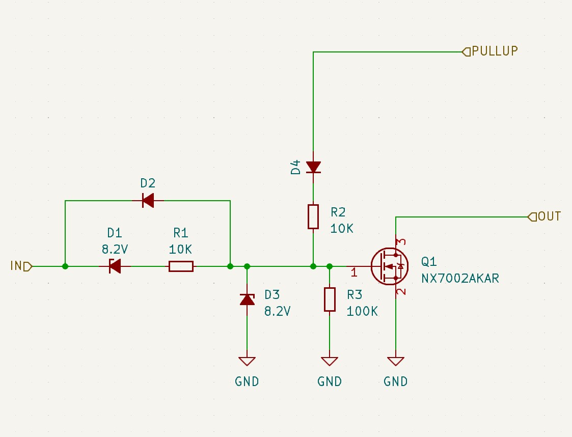
- The input (IN) at the left is where the wire is connected.
- The out (OUT) at the right goes to an MCU pin with enabled pull-up resistor.
- D1 and D3 are zener diodes.
- D2 and D4 are schottky diodes.
- Zener diodes value can be as lower as 4.7V
- PULLUP is a firmware controlled output. It can be the output of a power switch that gives 3.3V or a P-Channel mosfet working as a simple switch. It's not showing on the scematic because it will be common for all inputs. The circuit I represent will be multiplied 32 times. One for each input. 32 inputs total. All anodes of D4 will be connected together to the output of a power switch. That output will be firmware controlled using an mcu pin.
- How it works.
- When a voltage is applied (+24V typ) D1 conducts and Q1 starts conducting.
- D3 is used to protect gate-source maximum voltage.
- R3 is a pulldown.
- R1 limits the current through D1 and D3.
- When the IN is grounded D2 connects the gate to ground. It also cancels out R1 and D1 and the voltage divider that would be formed (R2 - R1). And brings gate source to ground.
- Firmware checks for Hi-Z.
- If we enable PULLUP, and the wire is floating. The state will change from Q1 not conducting to Q1 starts conducting. If the wire is connected to any other rails there will be no change. So, if a change occurs during the time the PULLUP is enabled the mcu translates that as "cable is floating".
- One mcu pin enables all PULLUP pins at the same time.
- This must be done multiple times per second but for my application that the frequency response is barely a 100Hz will do the job.
- The question:
- I don't like the D1 and D2 diodes.
- The reason I placed D1 is to avoid triggering the mosfet with very low voltage like 2V to 4V.
- Is D2 really necessary?
- What can I improve?
- EDIT:
- I drew an alternative circuit using BJT.
- 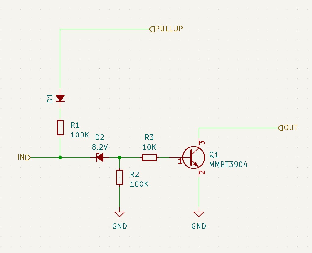
- In the second circuit, can the zener diode (D2) pull down the base of the transistor and turn it off?
- I want to sense 3 different states in the same mcu pin (GND, Hi-Z and PWR).
- PWR is typical +24V but I would like to have a wide margin from +17V to +40V just to be safe. The values can change but the typical will still be +24V
- I need 32 different (physical) inputs.
- I designed the following circuit after some brainstorming from my previous post and I'd like some review on it.
- 
- The input (IN) at the left is where the wire is connected.
- The out (OUT) at the right goes to an MCU pin with enabled pull-up resistor.
- D1 and D3 are zener diodes.
- D2 and D4 are schottky diodes.
- Zener diodes value can be as lower as 4.7V
- PULLUP is a firmware controlled output. It can be the output of a power switch that gives 3.3V or a P-Channel mosfet working as a simple switch. It's not showing on the scematic because it will be common for all inputs. The circuit I represent will be multiplied 32 times. One for each input. 32 inputs total. All anodes of D4 will be connected together to the output of a power switch. That output will be firmware controlled using an mcu pin.
- How it works.
- When a voltage is applied (+24V typ) D1 conducts and Q1 starts conducting.
- D3 is used to protect gate-source maximum voltage.
- R3 is a pulldown.
- R1 limits the current through D1 and D3.
- When the IN is grounded D2 connects the gate to ground. It also cancels out R1 and D1 and the voltage divider that would be formed (R2 - R1). And brings gate source to ground.
- Firmware checks for Hi-Z.
- If we enable PULLUP, and the wire is floating. The state will change from Q1 not conducting to Q1 starts conducting. If the wire is connected to any other rails there will be no change. So, if a change occurs during the time the PULLUP is enabled the mcu translates that as "cable is floating".
- One mcu pin enables all PULLUP pins at the same time.
- This must be done multiple times per second but for my application that the frequency response is barely a 100Hz will do the job.
- The question:
- I don't like the D1 and D2 diodes.
- The reason I placed D1 is to avoid triggering the mosfet with very low voltage like 2V to 4V.
- Is D2 really necessary?
- What can I improve?
- EDIT:
- I drew an alternative circuit using BJT.
- 
- In the second circuit. PULLUP pin must be +24V
- In the second circuit, can the zener diode (D2) pull down the base of the transistor and turn it off?
#10: Post edited
by
DeadMouse
·
2023-06-18T09:46:18Z (about 2 years ago)
- I want to sense 3 different states in the same mcu pin (GND, Hi-Z and PWR).
- PWR is typical +24V but I would like to have a wide margin from +17V to +40V just to be safe. The values can change but the typical will still be +24V
- I need 32 different (physical) inputs.
- I designed the following circuit after some brainstorming from my previous post and I'd like some review on it.
- 
- The input (IN) at the left is where the wire is connected.
- The out (OUT) at the right goes to an MCU pin with enabled pull-up resistor.
- D1 and D3 are zener diodes.
- D2 and D4 are schottky diodes.
- Zener diodes value can be as lower as 4.7V
- PULLUP is a firmware controlled output. It can be the output of a power switch that gives 3.3V or a P-Channel mosfet working as a simple switch. It's not showing on the scematic because it will be common for all inputs. The circuit I represent will be multiplied 32 times. One for each input. 32 inputs total. All anodes of D4 will be connected together to the output of a power switch. That output will be firmware controlled using an mcu pin.
- How it works.
- When a voltage is applied (+24V typ) D1 conducts and Q1 starts conducting.
- D3 is used to protect gate-source maximum voltage.
- R3 is a pulldown.
- R1 limits the current through D1 and D3.
- When the IN is grounded D2 connects the gate to ground. It also cancels out R1 and D1 and the voltage divider that would be formed (R2 - R1). And brings gate source to ground.
- Firmware checks for Hi-Z.
- If we enable PULLUP, and the wire is floating. The state will change from Q1 not conducting to Q1 starts conducting. If the wire is connected to any other rails there will be no change. So, if a change occurs during the time the PULLUP is enabled the mcu translates that as "cable is floating".
- One mcu pin enables all PULLUP pins at the same time.
- This must be done multiple times per second but for my application that the frequency response is barely a 100Hz will do the job.
- The question:
- I don't like the D1 and D2 diodes.
- The reason I placed D1 is to avoid triggering the mosfet with very low voltage like 2V to 4V.
- Is D2 really necessary?
- What can I improve?
- EDIT:
- I drew an alternative circuit using BJT.
- 
- In the second circuit, can the zener diode (D2) pull down the base of the transistor and turn it off?
#9: Post edited
by
DeadMouse
·
2023-06-18T09:44:51Z (about 2 years ago)
- I want to sense 3 different states in the same mcu pin (GND, Hi-Z and PWR).
- PWR is typical +24V but I would like to have a wide margin from +17V to +40V just to be safe. The values can change but the typical will still be +24V
- I need 32 different (physical) inputs.
- I designed the following circuit after some brainstorming from my previous post and I'd like some review on it.
- 
- The input (IN) at the left is where the wire is connected.
- The out (OUT) at the right goes to an MCU pin with enabled pull-up resistor.
- D1 and D3 are zener diodes.
- D2 and D4 are schottky diodes.
- Zener diodes value can be as lower as 4.7V
- PULLUP is a firmware controlled output. It can be the output of a power switch that gives 3.3V or a P-Channel mosfet working as a simple switch. It's not showing on the scematic because it will be common for all inputs. The circuit I represent will be multiplied 32 times. One for each input. 32 inputs total. All anodes of D4 will be connected together to the output of a power switch. That output will be firmware controlled using an mcu pin.
- How it works.
- When a voltage is applied (+24V typ) D1 conducts and Q1 starts conducting.
- D3 is used to protect gate-source maximum voltage.
- R3 is a pulldown.
- R1 limits the current through D1 and D3.
- When the IN is grounded D2 connects the gate to ground. It also cancels out R1 and D1 and the voltage divider that would be formed (R2 - R1). And brings gate source to ground.
- Firmware checks for Hi-Z.
- If we enable PULLUP, and the wire is floating. The state will change from Q1 not conducting to Q1 starts conducting. If the wire is connected to any other rails there will be no change. So, if a change occurs during the time the PULLUP is enabled the mcu translates that as "cable is floating".
- One mcu pin enables all PULLUP pins at the same time.
- This must be done multiple times per second but for my application that the frequency response is barely a 100Hz will do the job.
- The question:
- I don't like the D1 and D2 diodes.
- The reason I placed D1 is to avoid triggering the mosfet with very low voltage like 2V to 4V.
- Is D2 really necessary?
- What can I improve?
- EDIT:
- I drew an alternative circuit using BJT.
- 
#8: Post edited
by
DeadMouse
·
2023-06-17T19:06:11Z (about 2 years ago)
- I want to sense 3 different states in the same mcu pin (GND, Hi-Z and PWR).
- PWR is typical +24V but I would like to have a wide margin from +17V to +40V just to be safe. The values can change but the typical will still be +24V
- I need 32 different (physical) inputs.
- I designed the following circuit after some brainstorming from my previous post and I'd like some review on it.
- 
- The input (IN) at the left is where the wire is connected.
- The out (OUT) at the right goes to an MCU pin with enabled pull-up resistor.
- D1 and D3 are zener diodes.
- D2 and D4 are schottky diodes.
- PULLUP is a firmware controlled output. It can be the output of a power switch that gives 3.3V or a P-Channel mosfet working as a simple switch. It's not showing on the scematic because it will be common for all inputs. The circuit I represent will be multiplied 32 times. One for each input. 32 inputs total. All anodes of D4 will be connected together to the output of a power switch. That output will be firmware controlled using an mcu pin.
- How it works.
- When a voltage is applied (+24V typ) D1 conducts and Q1 starts conducting.
- D3 is used to protect gate-source maximum voltage.
- R3 is a pulldown.
- R1 limits the current through D1 and D3.
- When the IN is grounded D2 connects the gate to ground. It also cancels out R1 and D1 and the voltage divider that would be formed (R2 - R1). And brings gate source to ground.
- Firmware checks for Hi-Z.
- If we enable PULLUP, and the wire is floating. The state will change from Q1 not conducting to Q1 starts conducting. If the wire is connected to any other rails there will be no change. So, if a change occurs during the time the PULLUP is enabled the mcu translates that as "cable is floating".
- One mcu pin enables all PULLUP pins at the same time.
- This must be done multiple times per second but for my application that the frequency response is barely a 100Hz will do the job.
- The question:
- I don't like the D1 and D2 diodes.
- The reason I placed D1 is to avoid triggering the mosfet with very low voltage like 2V to 4V.
- Is D2 really necessary?
- What can I improve?
- I want to sense 3 different states in the same mcu pin (GND, Hi-Z and PWR).
- PWR is typical +24V but I would like to have a wide margin from +17V to +40V just to be safe. The values can change but the typical will still be +24V
- I need 32 different (physical) inputs.
- I designed the following circuit after some brainstorming from my previous post and I'd like some review on it.
- 
- The input (IN) at the left is where the wire is connected.
- The out (OUT) at the right goes to an MCU pin with enabled pull-up resistor.
- D1 and D3 are zener diodes.
- D2 and D4 are schottky diodes.
- Zener diodes value can be as lower as 4.7V
- PULLUP is a firmware controlled output. It can be the output of a power switch that gives 3.3V or a P-Channel mosfet working as a simple switch. It's not showing on the scematic because it will be common for all inputs. The circuit I represent will be multiplied 32 times. One for each input. 32 inputs total. All anodes of D4 will be connected together to the output of a power switch. That output will be firmware controlled using an mcu pin.
- How it works.
- When a voltage is applied (+24V typ) D1 conducts and Q1 starts conducting.
- D3 is used to protect gate-source maximum voltage.
- R3 is a pulldown.
- R1 limits the current through D1 and D3.
- When the IN is grounded D2 connects the gate to ground. It also cancels out R1 and D1 and the voltage divider that would be formed (R2 - R1). And brings gate source to ground.
- Firmware checks for Hi-Z.
- If we enable PULLUP, and the wire is floating. The state will change from Q1 not conducting to Q1 starts conducting. If the wire is connected to any other rails there will be no change. So, if a change occurs during the time the PULLUP is enabled the mcu translates that as "cable is floating".
- One mcu pin enables all PULLUP pins at the same time.
- This must be done multiple times per second but for my application that the frequency response is barely a 100Hz will do the job.
- The question:
- I don't like the D1 and D2 diodes.
- The reason I placed D1 is to avoid triggering the mosfet with very low voltage like 2V to 4V.
- Is D2 really necessary?
- What can I improve?
#7: Post edited
by
DeadMouse
·
2023-06-17T19:00:18Z (about 2 years ago)
- I want to sense 3 different states in the same mcu pin (GND, Hi-Z and PWR).
- PWR is typical +24V but I would like to have a wide margin from +17V to +40V just to be safe. The values can change but the typical will still be +24V
- I need 32 different (physical) inputs.
- I designed the following circuit after some brainstorming from my previous post and I'd like some review on it.
- 
- The input (IN) at the left is where the wire is connected.
- The out (OUT) at the right goes to an MCU pin with enabled pull-up resistor.
- D1 and D3 are zener diodes.
- D2 and D4 are schottky diodes.
PULLUP is a firmware controlled output. It can be the output of a power switch that gives 3.3V or a P-Channel mosfet working as a simple switch. It's not showing on the scematic because it will be common for all inputs. The circuit I represent will be multiplied 32 times. One for each input. 32 inputs total.- How it works.
- When a voltage is applied (+24V typ) D1 conducts and Q1 starts conducting.
- D3 is used to protect gate-source maximum voltage.
- R3 is a pulldown.
- R1 limits the current through D1 and D3.
- When the IN is grounded D2 connects the gate to ground. It also cancels out R1 and D1 and the voltage divider that would be formed (R2 - R1). And brings gate source to ground.
- Firmware checks for Hi-Z.
- If we enable PULLUP, and the wire is floating. The state will change from Q1 not conducting to Q1 starts conducting. If the wire is connected to any other rails there will be no change. So, if a change occurs during the time the PULLUP is enabled the mcu translates that as "cable is floating".
- One mcu pin enables all PULLUP pins at the same time.
- This must be done multiple times per second but for my application that the frequency response is barely a 100Hz will do the job.
- The question:
- I don't like the D1 and D2 diodes.
- The reason I placed D1 is to avoid triggering the mosfet with very low voltage like 2V to 4V.
- Is D2 really necessary?
- What can I improve?
- I want to sense 3 different states in the same mcu pin (GND, Hi-Z and PWR).
- PWR is typical +24V but I would like to have a wide margin from +17V to +40V just to be safe. The values can change but the typical will still be +24V
- I need 32 different (physical) inputs.
- I designed the following circuit after some brainstorming from my previous post and I'd like some review on it.
- 
- The input (IN) at the left is where the wire is connected.
- The out (OUT) at the right goes to an MCU pin with enabled pull-up resistor.
- D1 and D3 are zener diodes.
- D2 and D4 are schottky diodes.
- PULLUP is a firmware controlled output. It can be the output of a power switch that gives 3.3V or a P-Channel mosfet working as a simple switch. It's not showing on the scematic because it will be common for all inputs. The circuit I represent will be multiplied 32 times. One for each input. 32 inputs total. All anodes of D4 will be connected together to the output of a power switch. That output will be firmware controlled using an mcu pin.
- How it works.
- When a voltage is applied (+24V typ) D1 conducts and Q1 starts conducting.
- D3 is used to protect gate-source maximum voltage.
- R3 is a pulldown.
- R1 limits the current through D1 and D3.
- When the IN is grounded D2 connects the gate to ground. It also cancels out R1 and D1 and the voltage divider that would be formed (R2 - R1). And brings gate source to ground.
- Firmware checks for Hi-Z.
- If we enable PULLUP, and the wire is floating. The state will change from Q1 not conducting to Q1 starts conducting. If the wire is connected to any other rails there will be no change. So, if a change occurs during the time the PULLUP is enabled the mcu translates that as "cable is floating".
- One mcu pin enables all PULLUP pins at the same time.
- This must be done multiple times per second but for my application that the frequency response is barely a 100Hz will do the job.
- The question:
- I don't like the D1 and D2 diodes.
- The reason I placed D1 is to avoid triggering the mosfet with very low voltage like 2V to 4V.
- Is D2 really necessary?
- What can I improve?
#6: Post edited
by
DeadMouse
·
2023-06-17T18:56:26Z (about 2 years ago)
- I want to sense 3 different states in the same mcu pin (GND, Hi-Z and PWR).
- PWR is typical +24V but I would like to have a wide margin from +17V to +40V just to be safe. The values can change but the typical will still be +24V
- I need 32 different (physical) inputs.
- I designed the following circuit after some brainstorming from my previous post and I'd like some review on it.
- 
- The input (IN) at the left is where the wire is connected.
- The out (OUT) at the right goes to an MCU pin with enabled pull-up resistor.
D2 and D3 are zener diodes.- PULLUP is a firmware controlled output. It can be the output of a power switch that gives 3.3V or a P-Channel mosfet working as a simple switch. It's not showing on the scematic because it will be common for all inputs. The circuit I represent will be multiplied 32 times. One for each input. 32 inputs total.
- How it works.
- When a voltage is applied (+24V typ) D1 conducts and Q1 starts conducting.
- D3 is used to protect gate-source maximum voltage.
- R3 is a pulldown.
- R1 limits the current through D1 and D3.
- When the IN is grounded D2 connects the gate to ground. It also cancels out R1 and D1 and the voltage divider that would be formed (R2 - R1). And brings gate source to ground.
- Firmware checks for Hi-Z.
- If we enable PULLUP, and the wire is floating. The state will change from Q1 not conducting to Q1 starts conducting. If the wire is connected to any other rails there will be no change. So, if a change occurs during the time the PULLUP is enabled the mcu translates that as "cable is floating".
- One mcu pin enables all PULLUP pins at the same time.
- This must be done multiple times per second but for my application that the frequency response is barely a 100Hz will do the job.
- The question:
- I don't like the D1 and D2 diodes.
- The reason I placed D1 is to avoid triggering the mosfet with very low voltage like 2V to 4V.
- Is D2 really necessary?
- What can I improve?
- I want to sense 3 different states in the same mcu pin (GND, Hi-Z and PWR).
- PWR is typical +24V but I would like to have a wide margin from +17V to +40V just to be safe. The values can change but the typical will still be +24V
- I need 32 different (physical) inputs.
- I designed the following circuit after some brainstorming from my previous post and I'd like some review on it.
- 
- The input (IN) at the left is where the wire is connected.
- The out (OUT) at the right goes to an MCU pin with enabled pull-up resistor.
- D1 and D3 are zener diodes.
- D2 and D4 are schottky diodes.
- PULLUP is a firmware controlled output. It can be the output of a power switch that gives 3.3V or a P-Channel mosfet working as a simple switch. It's not showing on the scematic because it will be common for all inputs. The circuit I represent will be multiplied 32 times. One for each input. 32 inputs total.
- How it works.
- When a voltage is applied (+24V typ) D1 conducts and Q1 starts conducting.
- D3 is used to protect gate-source maximum voltage.
- R3 is a pulldown.
- R1 limits the current through D1 and D3.
- When the IN is grounded D2 connects the gate to ground. It also cancels out R1 and D1 and the voltage divider that would be formed (R2 - R1). And brings gate source to ground.
- Firmware checks for Hi-Z.
- If we enable PULLUP, and the wire is floating. The state will change from Q1 not conducting to Q1 starts conducting. If the wire is connected to any other rails there will be no change. So, if a change occurs during the time the PULLUP is enabled the mcu translates that as "cable is floating".
- One mcu pin enables all PULLUP pins at the same time.
- This must be done multiple times per second but for my application that the frequency response is barely a 100Hz will do the job.
- The question:
- I don't like the D1 and D2 diodes.
- The reason I placed D1 is to avoid triggering the mosfet with very low voltage like 2V to 4V.
- Is D2 really necessary?
- What can I improve?
#5: Post edited
by
DeadMouse
·
2023-06-17T18:55:33Z (about 2 years ago)
- I want to sense 3 different states in the same mcu pin (GND, Hi-Z and PWR).
- PWR is typical +24V but I would like to have a wide margin from +17V to +40V just to be safe. The values can change but the typical will still be +24V
- I need 32 different (physical) inputs.
- I designed the following circuit after some brainstorming from my previous post and I'd like some review on it.
- 
- The input (IN) at the left is where the wire is connected.
The out (OUT) at the right goes to an MCU pin with enabled pull-up resistor.- PULLUP is a firmware controlled output. It can be the output of a power switch that gives 3.3V or a P-Channel mosfet working as a simple switch. It's not showing on the scematic because it will be common for all inputs. The circuit I represent will be multiplied 32 times. One for each input. 32 inputs total.
- How it works.
- When a voltage is applied (+24V typ) D1 conducts and Q1 starts conducting.
- D3 is used to protect gate-source maximum voltage.
- R3 is a pulldown.
- R1 limits the current through D1 and D3.
- When the IN is grounded D2 connects the gate to ground. It also cancels out R1 and D1 and the voltage divider that would be formed (R2 - R1). And brings gate source to ground.
- Firmware checks for Hi-Z.
- If we enable PULLUP, and the wire is floating. The state will change from Q1 not conducting to Q1 starts conducting. If the wire is connected to any other rails there will be no change. So, if a change occurs during the time the PULLUP is enabled the mcu translates that as "cable is floating".
- One mcu pin enables all PULLUP pins at the same time.
- This must be done multiple times per second but for my application that the frequency response is barely a 100Hz will do the job.
- The question:
- I don't like the D1 and D2 diodes.
- The reason I placed D1 is to avoid triggering the mosfet with very low voltage like 2V to 4V.
- Is D2 really necessary?
What can I improve?
- I want to sense 3 different states in the same mcu pin (GND, Hi-Z and PWR).
- PWR is typical +24V but I would like to have a wide margin from +17V to +40V just to be safe. The values can change but the typical will still be +24V
- I need 32 different (physical) inputs.
- I designed the following circuit after some brainstorming from my previous post and I'd like some review on it.
- 
- The input (IN) at the left is where the wire is connected.
- The out (OUT) at the right goes to an MCU pin with enabled pull-up resistor.
- D2 and D3 are zener diodes.
- PULLUP is a firmware controlled output. It can be the output of a power switch that gives 3.3V or a P-Channel mosfet working as a simple switch. It's not showing on the scematic because it will be common for all inputs. The circuit I represent will be multiplied 32 times. One for each input. 32 inputs total.
- How it works.
- When a voltage is applied (+24V typ) D1 conducts and Q1 starts conducting.
- D3 is used to protect gate-source maximum voltage.
- R3 is a pulldown.
- R1 limits the current through D1 and D3.
- When the IN is grounded D2 connects the gate to ground. It also cancels out R1 and D1 and the voltage divider that would be formed (R2 - R1). And brings gate source to ground.
- Firmware checks for Hi-Z.
- If we enable PULLUP, and the wire is floating. The state will change from Q1 not conducting to Q1 starts conducting. If the wire is connected to any other rails there will be no change. So, if a change occurs during the time the PULLUP is enabled the mcu translates that as "cable is floating".
- One mcu pin enables all PULLUP pins at the same time.
- This must be done multiple times per second but for my application that the frequency response is barely a 100Hz will do the job.
- The question:
- I don't like the D1 and D2 diodes.
- The reason I placed D1 is to avoid triggering the mosfet with very low voltage like 2V to 4V.
- Is D2 really necessary?
- What can I improve?
#4: Post edited
by
DeadMouse
·
2023-06-17T18:54:31Z (about 2 years ago)
- I want to sense 3 different states in the same mcu pin (GND, Hi-Z and PWR).
- PWR is typical +24V but I would like to have a wide margin from +17V to +40V just to be safe. The values can change but the typical will still be +24V
- I need 32 different (physical) inputs.
- I designed the following circuit after some brainstorming from my previous post and I'd like some review on it.
- 
- The input (IN) at the left is where the wire is connected.
- The out (OUT) at the right goes to an MCU pin with enabled pull-up resistor.
- PULLUP is a firmware controlled output. It can be the output of a power switch that gives 3.3V or a P-Channel mosfet working as a simple switch. It's not showing on the scematic because it will be common for all inputs. The circuit I represent will be multiplied 32 times. One for each input. 32 inputs total.
- How it works.
- When a voltage is applied (+24V typ) D1 conducts and Q1 starts conducting.
- D3 is used to protect gate-source maximum voltage.
- R3 is a pulldown.
- R1 limits the current through D1 and D3.
- When the IN is grounded D2 connects the gate to ground. It also cancels out R1 and D1 and the voltage divider that would be formed (R2 - R1). And brings gate source to ground.
- Firmware checks for Hi-Z.
- If we enable PULLUP, and the wire is floating. The state will change from Q1 not conducting to Q1 starts conducting. If the wire is connected to any other rails there will be no change. So, if a change occurs during the time the PULLUP is enabled the mcu translates that as "cable is floating".
- One mcu pin enables all PULLUP pins at the same time.
- This must be done multiple times per second but for my application that the frequency response is barely a 100Hz will do the job.
- The question:
- I don't like the D1 and D2 diodes.
The reason I placed D1 is to avoid triggering the mosfet with very low voltage like 2V to 4V- Is D2 really necessary?
- What can I improve?
- I want to sense 3 different states in the same mcu pin (GND, Hi-Z and PWR).
- PWR is typical +24V but I would like to have a wide margin from +17V to +40V just to be safe. The values can change but the typical will still be +24V
- I need 32 different (physical) inputs.
- I designed the following circuit after some brainstorming from my previous post and I'd like some review on it.
- 
- The input (IN) at the left is where the wire is connected.
- The out (OUT) at the right goes to an MCU pin with enabled pull-up resistor.
- PULLUP is a firmware controlled output. It can be the output of a power switch that gives 3.3V or a P-Channel mosfet working as a simple switch. It's not showing on the scematic because it will be common for all inputs. The circuit I represent will be multiplied 32 times. One for each input. 32 inputs total.
- How it works.
- When a voltage is applied (+24V typ) D1 conducts and Q1 starts conducting.
- D3 is used to protect gate-source maximum voltage.
- R3 is a pulldown.
- R1 limits the current through D1 and D3.
- When the IN is grounded D2 connects the gate to ground. It also cancels out R1 and D1 and the voltage divider that would be formed (R2 - R1). And brings gate source to ground.
- Firmware checks for Hi-Z.
- If we enable PULLUP, and the wire is floating. The state will change from Q1 not conducting to Q1 starts conducting. If the wire is connected to any other rails there will be no change. So, if a change occurs during the time the PULLUP is enabled the mcu translates that as "cable is floating".
- One mcu pin enables all PULLUP pins at the same time.
- This must be done multiple times per second but for my application that the frequency response is barely a 100Hz will do the job.
- The question:
- I don't like the D1 and D2 diodes.
- The reason I placed D1 is to avoid triggering the mosfet with very low voltage like 2V to 4V.
- Is D2 really necessary?
- What can I improve?
#3: Post edited
by
DeadMouse
·
2023-06-17T18:53:51Z (about 2 years ago)
- I want to sense 3 different states in the same mcu pin (GND, Hi-Z and PWR).
- PWR is typical +24V but I would like to have a wide margin from +17V to +40V just to be safe. The values can change but the typical will still be +24V
- I need 32 different (physical) inputs.
- I designed the following circuit after some brainstorming from my previous post and I'd like some review on it.
- 
- The input (IN) at the left is where the wire is connected.
- The out (OUT) at the right goes to an MCU pin with enabled pull-up resistor.
- PULLUP is a firmware controlled output. It can be the output of a power switch that gives 3.3V or a P-Channel mosfet working as a simple switch. It's not showing on the scematic because it will be common for all inputs. The circuit I represent will be multiplied 32 times. One for each input. 32 inputs total.
- How it works.
- When a voltage is applied (+24V typ) D1 conducts and Q1 starts conducting.
- D3 is used to protect gate-source maximum voltage.
- R3 is a pulldown.
- R1 limits the current through D1 and D3.
- When the IN is grounded D2 connects the gate to ground. It also cancels out R1 and D1 and the voltage divider that would be formed (R2 - R1). And brings gate source to ground.
- Firmware checks for Hi-Z.
- If we enable PULLUP, and the wire is floating. The state will change from Q1 not conducting to Q1 starts conducting. If the wire is connected to any other rails there will be no change. So, if a change occurs during the time the PULLUP is enabled the mcu translates that as "cable is floating".
- One mcu pin enables all PULLUP pins at the same time.
- This must be done multiple times per second but for my application that the frequency response is barely a 100Hz will do the job.
- The question:
- I don't like the D1 and D2 diodes.
The reason I places D1 is to avoid triggering the mosfet with very low voltage like 2V to 4V- Is D2 really necessary?
- What can I improve?
- I want to sense 3 different states in the same mcu pin (GND, Hi-Z and PWR).
- PWR is typical +24V but I would like to have a wide margin from +17V to +40V just to be safe. The values can change but the typical will still be +24V
- I need 32 different (physical) inputs.
- I designed the following circuit after some brainstorming from my previous post and I'd like some review on it.
- 
- The input (IN) at the left is where the wire is connected.
- The out (OUT) at the right goes to an MCU pin with enabled pull-up resistor.
- PULLUP is a firmware controlled output. It can be the output of a power switch that gives 3.3V or a P-Channel mosfet working as a simple switch. It's not showing on the scematic because it will be common for all inputs. The circuit I represent will be multiplied 32 times. One for each input. 32 inputs total.
- How it works.
- When a voltage is applied (+24V typ) D1 conducts and Q1 starts conducting.
- D3 is used to protect gate-source maximum voltage.
- R3 is a pulldown.
- R1 limits the current through D1 and D3.
- When the IN is grounded D2 connects the gate to ground. It also cancels out R1 and D1 and the voltage divider that would be formed (R2 - R1). And brings gate source to ground.
- Firmware checks for Hi-Z.
- If we enable PULLUP, and the wire is floating. The state will change from Q1 not conducting to Q1 starts conducting. If the wire is connected to any other rails there will be no change. So, if a change occurs during the time the PULLUP is enabled the mcu translates that as "cable is floating".
- One mcu pin enables all PULLUP pins at the same time.
- This must be done multiple times per second but for my application that the frequency response is barely a 100Hz will do the job.
- The question:
- I don't like the D1 and D2 diodes.
- The reason I placed D1 is to avoid triggering the mosfet with very low voltage like 2V to 4V
- Is D2 really necessary?
- What can I improve?
#2: Post edited
by
DeadMouse
·
2023-06-17T18:52:21Z (about 2 years ago)
- I want to sense 3 different states in the same mcu pin (GND, Hi-Z and PWR).
- PWR is typical +24V but I would like to have a wide margin from +17V to +40V just to be safe. The values can change but the typical will still be +24V
I need 32 different inputs.- I designed the following circuit after some brainstorming from my previous post and I'd like some review on it.
- 
- The input (IN) at the left is where the wire is connected.
- The out (OUT) at the right goes to an MCU pin with enabled pull-up resistor.
- PULLUP is a firmware controlled output. It can be the output of a power switch that gives 3.3V or a P-Channel mosfet working as a simple switch. It's not showing on the scematic because it will be common for all inputs. The circuit I represent will be multiplied 32 times. One for each input. 32 inputs total.
- How it works.
- When a voltage is applied (+24V typ) D1 conducts and Q1 starts conducting.
- D3 is used to protect gate-source maximum voltage.
- R3 is a pulldown.
- R1 limits the current through D1 and D3.
- When the IN is grounded D2 connects the gate to ground. It also cancels out R1 and D1 and the voltage divider that would be formed (R2 - R1). And brings gate source to ground.
- Firmware checks for Hi-Z.
- If we enable PULLUP, and the wire is floating. The state will change from Q1 not conducting to Q1 starts conducting. If the wire is connected to any other rails there will be no change. So, if a change occurs during the time the PULLUP is enabled the mcu translates that as "cable is floating".
This must be done multiple times per second but for my application that the frequency response is barely a 100Hz will do the job.- The question:
- I don't like the D1 and D2 diodes.
- The reason I places D1 is to avoid triggering the mosfet with very low voltage like 2V to 4V
- Is D2 really necessary?
- What can I improve?
- I want to sense 3 different states in the same mcu pin (GND, Hi-Z and PWR).
- PWR is typical +24V but I would like to have a wide margin from +17V to +40V just to be safe. The values can change but the typical will still be +24V
- I need 32 different (physical) inputs.
- I designed the following circuit after some brainstorming from my previous post and I'd like some review on it.
- 
- The input (IN) at the left is where the wire is connected.
- The out (OUT) at the right goes to an MCU pin with enabled pull-up resistor.
- PULLUP is a firmware controlled output. It can be the output of a power switch that gives 3.3V or a P-Channel mosfet working as a simple switch. It's not showing on the scematic because it will be common for all inputs. The circuit I represent will be multiplied 32 times. One for each input. 32 inputs total.
- How it works.
- When a voltage is applied (+24V typ) D1 conducts and Q1 starts conducting.
- D3 is used to protect gate-source maximum voltage.
- R3 is a pulldown.
- R1 limits the current through D1 and D3.
- When the IN is grounded D2 connects the gate to ground. It also cancels out R1 and D1 and the voltage divider that would be formed (R2 - R1). And brings gate source to ground.
- Firmware checks for Hi-Z.
- If we enable PULLUP, and the wire is floating. The state will change from Q1 not conducting to Q1 starts conducting. If the wire is connected to any other rails there will be no change. So, if a change occurs during the time the PULLUP is enabled the mcu translates that as "cable is floating".
- One mcu pin enables all PULLUP pins at the same time.
- This must be done multiple times per second but for my application that the frequency response is barely a 100Hz will do the job.
- The question:
- I don't like the D1 and D2 diodes.
- The reason I places D1 is to avoid triggering the mosfet with very low voltage like 2V to 4V
- Is D2 really necessary?
- What can I improve?
#1: Initial revision
by
DeadMouse
·
2023-06-17T18:50:01Z (about 2 years ago)
Sensing 3 states in a single mcu pin using firmware
I want to sense 3 different states in the same mcu pin (GND, Hi-Z and PWR). PWR is typical +24V but I would like to have a wide margin from +17V to +40V just to be safe. The values can change but the typical will still be +24V I need 32 different inputs. I designed the following circuit after some brainstorming from my previous post and I'd like some review on it.  The input (IN) at the left is where the wire is connected. The out (OUT) at the right goes to an MCU pin with enabled pull-up resistor. PULLUP is a firmware controlled output. It can be the output of a power switch that gives 3.3V or a P-Channel mosfet working as a simple switch. It's not showing on the scematic because it will be common for all inputs. The circuit I represent will be multiplied 32 times. One for each input. 32 inputs total. How it works. When a voltage is applied (+24V typ) D1 conducts and Q1 starts conducting. D3 is used to protect gate-source maximum voltage. R3 is a pulldown. R1 limits the current through D1 and D3. When the IN is grounded D2 connects the gate to ground. It also cancels out R1 and D1 and the voltage divider that would be formed (R2 - R1). And brings gate source to ground. Firmware checks for Hi-Z. If we enable PULLUP, and the wire is floating. The state will change from Q1 not conducting to Q1 starts conducting. If the wire is connected to any other rails there will be no change. So, if a change occurs during the time the PULLUP is enabled the mcu translates that as "cable is floating". This must be done multiple times per second but for my application that the frequency response is barely a 100Hz will do the job. The question: I don't like the D1 and D2 diodes. The reason I places D1 is to avoid triggering the mosfet with very low voltage like 2V to 4V Is D2 really necessary? What can I improve?