Post History
You have mentioned a few points yourself, so I will try to comment on those points and perhaps suggest some reasons to add or not to add a ground plane. You mentioned twisting (I suppose warping) ...
#3: Post edited
by
 Elleanor Lopez
·
2023-06-28T18:07:28Z (almost 2 years ago)
Elleanor Lopez
·
2023-06-28T18:07:28Z (almost 2 years ago)
- You have mentioned a few points yourself, so I will try to comment on those points and perhaps suggest some reasons to add or not to add a ground plane.
- You mentioned twisting (I suppose warping) of the board. I believe there is a chance this happens if the board is not symmetrical copper wise, so if you pour copper only on one of the outer layers you risk having the board warp.
- Another thing that can happen is high current density in certain board parts during electroplating process. Image is from EuroCircuits website on the topic of plating index:
- 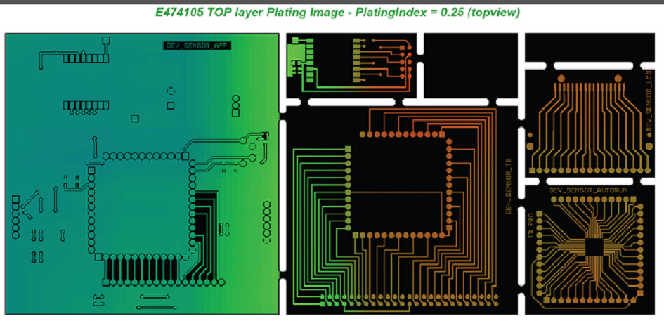
- In red are the areas that will be overplated.
- Having copper pour will help to equally distribute current across the surface, so you won't have overplated and underplated sections. As far as I have read, they try to mitigate this by placing thief copper outside the panel, and if there still is a potential problem they might ask if they can add thief copper onto your board as well.
- Yes, if you decide to pour copper on top, you have to make sure you don't create ground loops. You have to be in control of where the current returns to source, do not leave it up to chance. And you have to stitch them together with considerable amount of vias to ensure low impedance path between the planes, but within reason, because in mass production you might have to pay for extra vias.
- 
- Another thing to keep in mind is that pouring ground between traces without having a few vias stitching that ground sliver to the main ground plane can actually make things worse. If the connection to ground plane is far enough,it can start coupling noise between these two signals, that otherwise maybe would have been appropriately spaced.
- So if your ground pour on top layer is the 'guard trace', make sure it is terminated on both ends as a minimum, ideally with more vias on the way.
- Added bonus is additional plane capacitance between layers 3 and 4, which may or may not matter, better heat conduction, and as you mentioned yourself, less milling and waste.
- I see that you mention your traces are on top and bottom. Using the same stackup, I have used the power layer to route a sensitive analogue trace, and ground pour on layer 2 and layer 4 essentially shield it from the outside. But this was done in one small section of the board which did not split the power plane.
- Last, but not least, if you want to leave outer layers without ground plane and worry about manufacturing, the best thing to do is contact your PCB house and ask them if they can produce it or see any issues with it.
- You have mentioned a few points yourself, so I will try to comment on those points and perhaps suggest some reasons to add or not to add a ground plane.
- You mentioned twisting (I suppose warping) of the board. I believe there is a chance this happens if the board is not symmetrical copper wise, so if you pour copper only on one of the outer layers you risk having the board warp.
- Another thing that can happen is high current density in certain board parts during electroplating process. Image is from EuroCircuits website on the topic of plating index:
- 
- In red are the areas that will be overplated.
- Having copper pour will help to equally distribute current across the surface, so you won't have overplated and underplated sections. As far as I have read, they try to mitigate this by placing thief copper outside the panel, and if there still is a potential problem they might ask if they can add thief copper onto your board as well.
- Yes, if you decide to pour copper on top, you have to make sure you don't create ground loops. You have to be in control of where the current returns to source, do not leave it up to chance. And you have to stitch them together with considerable amount of vias to ensure low impedance path between the planes, but within reason, because in mass production you might have to pay for extra vias.
- 
- Another thing to keep in mind is that pouring ground between traces without having a few vias stitching that ground sliver to the main ground plane can actually make things worse. If the connection to ground plane is far enough,it can start coupling noise between these two signals, that otherwise maybe would have been appropriately spaced.
- So if your ground pour on top layer is the 'guard trace', make sure it is terminated on both ends as a minimum, ideally with more vias on the way.
- Added bonus is additional plane capacitance between layers 3 and 4, which may or may not matter, better heat conduction, and as you mentioned yourself, less milling and waste.
- I see that you mention your traces are on top and bottom. Using the same stackup, I have used the power layer to route a sensitive analogue trace, and ground pour on layer 2 and layer 4 essentially shield it from the outside. But this was done in one small section of the board which did not split the power plane.
- One notable exception can be if the PCB has to work in low outgassing environment like some vacuum applications. The requirements are stringent, and in general you want to reduce the amount of material on the outer layers, removing everything that is not strictly necessary.
- Last, but not least, if you want to leave outer layers without ground plane and worry about manufacturing, the best thing to do is contact your PCB house and ask them if they can produce it or see any issues with it.
- So in summary, I almost always fill the layers with copper, be it ground or power, but drawing a rectangle and pressing 'pour' will likely bring more sorrow than happiness. As long as you keep the aforementioned points in mind, as well as those mentioned by yourself, pouring seems superior option to me in most cases.
#2: Post edited
by
Elleanor Lopez
·
2023-06-28T18:00:49Z (almost 2 years ago)
- You have mentioned a few points yourself, so I will try to comment on those points and perhaps suggest some reasons to add or not to add a ground plane.
- You mentioned twisting (I suppose warping) of the board. I believe there is a chance this happens if the board is not symmetrical copper wise, so if you pour copper only on one of the outer layers you risk having the board warp.
- Another thing that can happen is high current density in certain board parts during electroplating process. Image is from EuroCircuits website on the topic of plating index:
- 
- Having copper pour will help to equally distribute current across the surface, so you won't have overplated and underplated sections. As far as I have read, they try to mitigate this by placing thief copper outside the panel, and if there still is a potential problem they might ask if they can add thief copper onto your board as well.
- Yes, if you decide to pour copper on top, you have to make sure you don't create ground loops. You have to be in control of where the current returns to source, do not leave it up to chance. And you have to stitch them together with considerable amount of vias to ensure low impedance path between the planes, but within reason, because in mass production you might have to pay for extra vias.
- 
- Another thing to keep in mind is that pouring ground between traces without having a few vias stitching that ground sliver to the main ground plane can actually make things worse. If the connection to ground plane is far enough,it can start coupling noise between these two signals, that otherwise maybe would have been appropriately spaced.
- So if your ground pour on top layer is the 'guard trace', make sure it is terminated on both ends as a minimum, ideally with more vias on the way.
- Added bonus is additional plane capacitance between layers 3 and 4, which may or may not matter, better heat conduction, and as you mentioned yourself, less milling and waste.
- I see that you mention your traces are on top and bottom. Using the same stackup, I have used the power layer to route a sensitive analogue trace, and ground pour on layer 2 and layer 4 essentially shield it from the outside. But this was done in one small section of the board which did not split the power plane.
- Last, but not least, if you want to leave outer layers without ground plane and worry about manufacturing, the best thing to do is contact your PCB house and ask them if they can produce it or see any issues with it.
- You have mentioned a few points yourself, so I will try to comment on those points and perhaps suggest some reasons to add or not to add a ground plane.
- You mentioned twisting (I suppose warping) of the board. I believe there is a chance this happens if the board is not symmetrical copper wise, so if you pour copper only on one of the outer layers you risk having the board warp.
- Another thing that can happen is high current density in certain board parts during electroplating process. Image is from EuroCircuits website on the topic of plating index:
- 
- In red are the areas that will be overplated.
- Having copper pour will help to equally distribute current across the surface, so you won't have overplated and underplated sections. As far as I have read, they try to mitigate this by placing thief copper outside the panel, and if there still is a potential problem they might ask if they can add thief copper onto your board as well.
- Yes, if you decide to pour copper on top, you have to make sure you don't create ground loops. You have to be in control of where the current returns to source, do not leave it up to chance. And you have to stitch them together with considerable amount of vias to ensure low impedance path between the planes, but within reason, because in mass production you might have to pay for extra vias.
- 
- Another thing to keep in mind is that pouring ground between traces without having a few vias stitching that ground sliver to the main ground plane can actually make things worse. If the connection to ground plane is far enough,it can start coupling noise between these two signals, that otherwise maybe would have been appropriately spaced.
- So if your ground pour on top layer is the 'guard trace', make sure it is terminated on both ends as a minimum, ideally with more vias on the way.
- Added bonus is additional plane capacitance between layers 3 and 4, which may or may not matter, better heat conduction, and as you mentioned yourself, less milling and waste.
- I see that you mention your traces are on top and bottom. Using the same stackup, I have used the power layer to route a sensitive analogue trace, and ground pour on layer 2 and layer 4 essentially shield it from the outside. But this was done in one small section of the board which did not split the power plane.
- Last, but not least, if you want to leave outer layers without ground plane and worry about manufacturing, the best thing to do is contact your PCB house and ask them if they can produce it or see any issues with it.
#1: Initial revision
by
Elleanor Lopez
·
2023-06-28T17:59:33Z (almost 2 years ago)
You have mentioned a few points yourself, so I will try to comment on those points and perhaps suggest some reasons to add or not to add a ground plane. You mentioned twisting (I suppose warping) of the board. I believe there is a chance this happens if the board is not symmetrical copper wise, so if you pour copper only on one of the outer layers you risk having the board warp. Another thing that can happen is high current density in certain board parts during electroplating process. Image is from EuroCircuits website on the topic of plating index:  Having copper pour will help to equally distribute current across the surface, so you won't have overplated and underplated sections. As far as I have read, they try to mitigate this by placing thief copper outside the panel, and if there still is a potential problem they might ask if they can add thief copper onto your board as well. Yes, if you decide to pour copper on top, you have to make sure you don't create ground loops. You have to be in control of where the current returns to source, do not leave it up to chance. And you have to stitch them together with considerable amount of vias to ensure low impedance path between the planes, but within reason, because in mass production you might have to pay for extra vias.  Another thing to keep in mind is that pouring ground between traces without having a few vias stitching that ground sliver to the main ground plane can actually make things worse. If the connection to ground plane is far enough,it can start coupling noise between these two signals, that otherwise maybe would have been appropriately spaced. So if your ground pour on top layer is the 'guard trace', make sure it is terminated on both ends as a minimum, ideally with more vias on the way. Added bonus is additional plane capacitance between layers 3 and 4, which may or may not matter, better heat conduction, and as you mentioned yourself, less milling and waste. I see that you mention your traces are on top and bottom. Using the same stackup, I have used the power layer to route a sensitive analogue trace, and ground pour on layer 2 and layer 4 essentially shield it from the outside. But this was done in one small section of the board which did not split the power plane. Last, but not least, if you want to leave outer layers without ground plane and worry about manufacturing, the best thing to do is contact your PCB house and ask them if they can produce it or see any issues with it.