What material is used in the tabs of power packages? (TO-220, D2PAK, etc.)
What material is used in the tabs of power packages? (TO-220, D2PAK, etc.)
I would assume probably a tin-plated copper alloy, but I can't find a reference. Datasheets don't seem to mention the material, aside from being lead-free.
See for example:
1 answer
A definitive answer is hard to give, since the information is not easily available. However, after a bit of research I'm inclined to believe that the most common materials are copper, copper alloys or sometimes Fe-Ni alloys, plated with some other material to prevent oxidation.
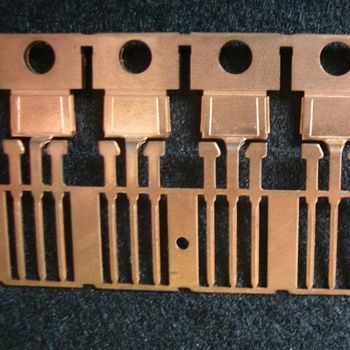
Note that the tab is an integral part of the lead frame of the device, and it turns out that there is quite a bit of technology in manufacturing lead frames like these:
What follows are the results of my research that back up my opening statement.
The following is an excerpt from the first part of patent application US5557842 – Method of manufacturing a semiconductor leadframe structure (emphasis mine):
Current leadframes for power semiconductor device packages (e.g., TO-218, TO-220, DPAK, D2 PAK, D3 PAK) typically are formed or stamped from a ribbon of a single or dual gauge metal material such as copper or a copper alloy. Typically, prior to stamping, all or part of the ribbon material is plated with another metal. After stamping, a typical power semiconductor leadframe comprises a die bond pad and a plurality of leads either connected to the die bond pad or in proximity to it. All or some of the leads include a bond post portion for connecting (e.g., wire bonding) a semiconductor die to the leads.
There is also this patent:Lead frame material and lead frame for semiconductor device. Its abstract says (emphasis mine):
A lead frame material comprises a base plate consisting of copper or copper alloys, and a protective coating formed on the upper or the both surface of the base plate. The protective coating is composed of at least one metal selected from the group consisting of gold, gold alloy, silver, silver alloy, palladium and palladium alloy, and has a thickness of 10-500 angstrom. The protective coating is formed by means of vapor deposition. It is possible to form an intermediate coating of nickel or nickel alloys between the surface of the base plate and the protective coating, by means of vapor deposition or wet plating. The suitable thickness of the intermediate coating is within the range of 50-20000 angstrom.
Another document reports the following (emphasis mine):
Plating
Common lead-frame materials are copper alloys (usually with a small percentage of iron) and ‘Alloy 42’, which is an alloy of iron (58% and nickel (42%). These materials have a close TCE match with silicon and good strength and workability. Bondability is generally enhanced by spot plating with silver. Lead-frames are generally not plated overall before assembly, and a solder surface would in any case not be compatible with the high temperatures involved in encapsulation by transfer moulding. This means that the package exterior must be solder-coated, either by hot dipping or plating. Hot dipping is effective, but difficult to control, with fine pitch surface mount parts being liable to solder bridging and variations in coating thickness which lead to problems of package non-coplanarity. As the parts are connected together and shorted out by the lead-frame, electrolytic plating is an option, a typical finish being 10μm of tin-lead. Depending on the application, either eutectic or 70/30 material can be specified, and the finish may be infra-red reflowed. The predominant finish is as-plated, having a dull grey appearance. Brighter finishes can be achieved by using plating additives, but, as with all plating operations, these may adversely affect solderability and ageing characteristics. Post-encapsulation plating is effective, but there is always the danger that plating chemical residues will impair the long-term reliability of the component. One alternative, which has been evaluated with some success, is to pre-plate the lead-frame with palladium on top of a nickel under-layer. Palladium increases adhesion to the encapsulant, and is dispersed during soldering to leave a bond between the solder and the underlying nickel. Unfortunately, the surface finish is poor, which discourages users.
0 comment threads

0 comment threads