Comments on Using FET based followers and design rules
Parent
Using FET based followers and design rules
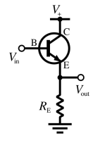
Usually, voltage followers are built with bipolar transistors (or with opamps if better precision is needed). In this case, the simple rule says that the transistor emitter "follows" the input voltage one diode drop below, a somewhat approximate but understandable term.
It is perhaps less usual to see field effect based followers, and I'm particularly interested in jfets and mosfets.
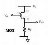
From my readings about this topic, it is still unclear to me how to determine the voltage drop introduced by these transistors (parallel to the diode drop for the bipolar transistor follower).
Also, if there is a way to control this drop (without using an opamp), what are the design rules, or perhaps the rules of thumbs ?
Allow me to address the MOSFET only as a source follower. - this has very unpredictable linear use without voltage …
4y ago
"Also, if there is a way to control this drop (without using an oamp), what are the design rules, or perhaps the rules o …
4y ago
FET source-followers are generally less predictable than BJT (bipolar junction transistor, like NPN or PNP) emitter-foll …
4y ago
> ... it is still unclear to me how to determine the voltage drop introduced by these transistors... Very interesting …
4y ago
In addition to Olin's answer: > and I'm particularly interested in jfets and mosfets. If you decide to go dow …
4y ago
Post
... it is still unclear to me how to determine the voltage drop introduced by these transistors...
Very interesting question... I have asked myself many times in the past... and I have not been able to answer it... but now I think I have already succeeded... Maybe Codidact acts as a kind of "catalyst" for my creative thinking:) In addition, the principle of negative feedback and Mr Hayes with his Student Manual for the Art of Electronics (my favorite book from the past) helped me realize the idea.
"Negative feedback" here means that the transistor (JFET) passes its drain current through the source resistor thus trying to increase the voltage drop across it. But this voltage is applied to the gate-source junction so that to decrease the drain current. As a result, equilibrium is achieved. And the OP's question is, "How much is VGS?" I would ask the same about ID. So we need to know both...
It is obvious the question is about a large DC input signal varying between the supply rails. The transfer characteristic Id = f(Vgs) is nonlinear and the transconductance gm cannot be used. Then Mr Hayes suggested solving the circuit graphically. I have extracted below three consecutive steps from his explanations. Let's consider them.
1. Simplest JFET current source. Compared with BJT, JFET is a weird device because it has an NP junction but it is backward biased... and the transistor is fully on when the voltage across this junction is zero. To make it zero, we can simply join the gate and source (Fig. 1 left), thus obtaining the simplest possible JFET current source. This connection is very useful in this application since the 3-terminal transistor is made act as a 2-terminal current-stabilizing "diode".
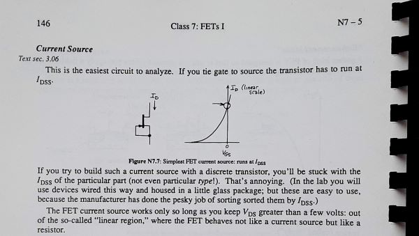
Fig. 1. To make VGS - 0, we can simply join the gate and source.
The intersection point between two curves (the JFET's IV curve and the ordinate axis) gives the graphical solution (Fig. 1 right). There is no negative feedback in this arrangement.
2. Self-biased JFET current source. To set the desired current, we can insert a source resistor Rs (between the gate and source) - Fig. 2 left. The negative feedback comes into picture (as I have explained it above) and the equilibrium is reached. It is interesting to see the graphical solution for this case - Fig. 2 right.
Fig. 2. Self-biased JFET current source.
I had a problem understanding this graphical interpretation because I had the usual idea of this visualization technique - the curves of two elements (for example a diode and a resistor) overlap in the same coordinate system and their intersection (operating) point gives the solution. But they are "ordinary" elements with two terminals between which the current passes and voltage drop appears.
The problem here is that the one of them is a "trans element" since the voltage appears across one place but the current flows through other place. But the trick here is that, for the purposes of this graphical presentation, it is thought of as a "composed" 2-terminal element with its nonlinear IV curve. It is as if both the current and the voltage are its... but that is just an illusion.
The "trans element" can be considered as a virtual element whose voltage is the original VGS but the current Id is artificially created according to the trans curve.
Note the resistor is represented by a reversed IV curve (line). The intersection point between it and the JFET transfer curve gives an answer to the OP's question.
3. Self-biased JFET source follower. The situations above were static. Let's now include an input voltage. We can do it in various ways - as in Fig. 3 through a capacitor (small AC)... or just connecting the input voltage source between the gate and ground (in series to the gate-source junction). Thus its voltage will be added/subtracted to/from the voltage drop across the resistor.
Fig. 3. Self-biased JFET source follower.
It is interesting to imagine what the graphical interpretation will be (Mr. Hayes has not provided us with an illustration; so we will have to imagine it ourselves). I think the JFET IV curve will move horizontally (translate)... and the intersection point will move along the R IV curve (the "load line"). It would be good to draw it... OK, let's do it.
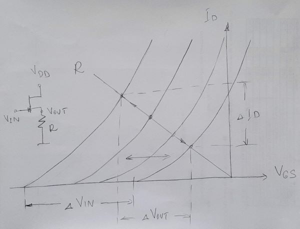
Fig. 4. JFET source follower with Vin (quickly sketched)
But why not use the same technique to show the operation of the classic emitter follower?
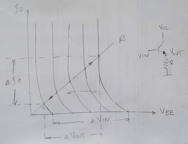
Fig. 5. Emitter follower with Vin (quickly sketched)
Note the transistor is represented by a reversed IV transfer curve. Here the "trans element" can be considered as a virtual element whose original current IB is modified by adding beta x IB current to it.
And here is another challenge for your imagination - the same two pictures but with additionally shown "dynamic resistance" RDS and RCE (thin lines starting from the beginning of each IV curve and crossing the operating point).
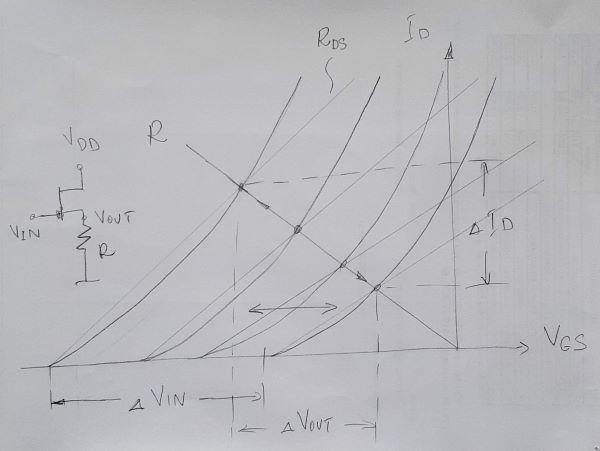
Fig. 6. JFET source follower with dynamic resistance RDS visualized
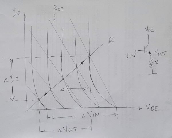
Fig. 7. Emitter follower with dynamic resistance RCE visualized
If necessary, I will add more explanations to the last two figures to clarify how the non-linear transfer curve is obtained by the concept of "dynamic resistance"...

1 comment thread