Comments on Isolated Digital Input - Overvoltage protection
Parent
Isolated Digital Input - Overvoltage protection
I am trying to build an active-low digital isolated switch capable of withstanding 32VDC voltage without creating any damage to the system.
This is the snapshot of the circuit not fulfilling the requirement:
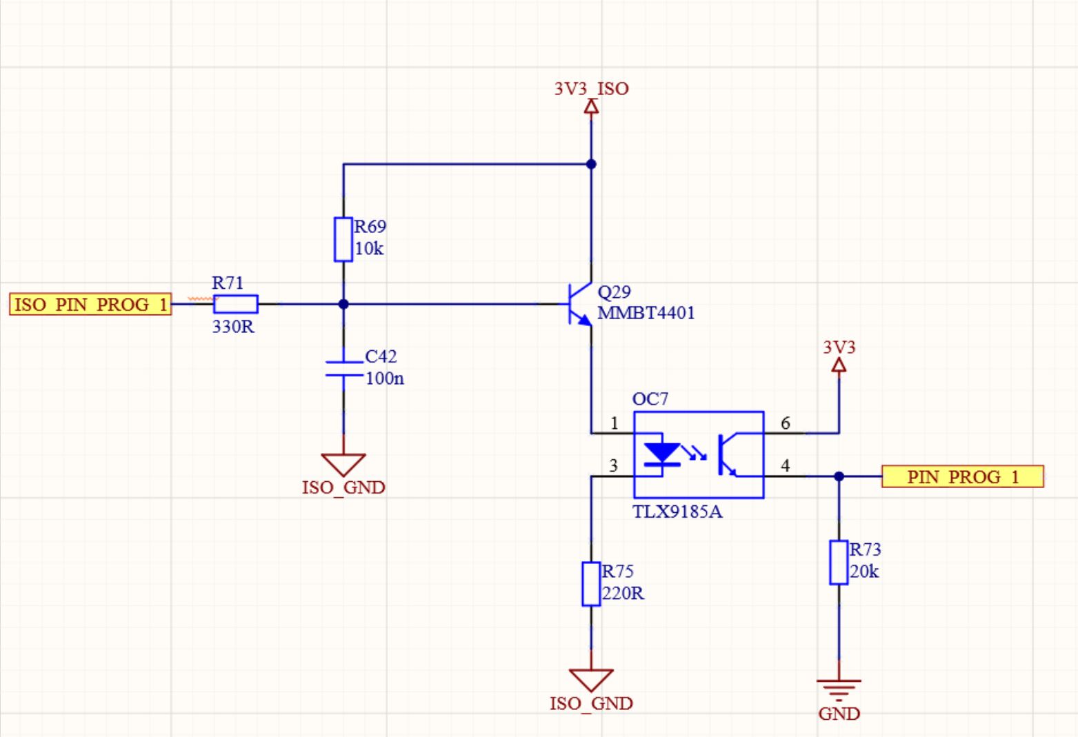
"ISO_PIN_PROG_1" will be connected to the switch which will tie to the ground and causing the base of the Q29 to go below 0.7V hence cutting off the OC7.
"PIN_PROG_1" will be connected to the MCU input.
If there is a 32V applied by the accident on "ISO_PIN_PROG_1" this would cause problems with the circuit as is. How could I properly solve it?
-
Step 1: Since 3V3_ISO would be LDO driven I would probably add a diode with the anode connected to the LDO output and a cathode connected with the LDO input to prevent the LDO to have output higher than the input. Based on my experience they tend not to love that. I haven't post that because I haven't yet designed the power stage.
-
Step 2: Add Zener regulator at i.e. 12V with a properly dimensioned resistor and add one more resistor in series with Q29 base to limit the current - does it need to be limited because there is a limit how high Ic of the Q29 could be in full saturation? I believe it should because it won't be in the forward active region anymore.
I may be stuck having multiple unknowns and not being really secure whether this is the right topology for the task and whether I am addressing the problems correctly so your help would be kindly appreciated! Thanks as always!
Further clarifications ——————————————————————————
When input is left floating opto’s diode is forward biased as seen on the schematic. When input is low, the opto should be off therefore “PIN_PROG_1” should be high. That is really all in terms of usual usage. However, there is a chance that someone would connect 32V max on the input and without adding any support the circuit shown would be damaged. Proper operation during the event is not needed - so when between 3V3 and 32V on the Q29 base circuit and PSU should not be damaged, output of it is less important. Snap on action is not required. Esd protection is important. Input impedance should be high.
Post
Step 1: Since 3V3_ISO would be LDO driven I would probably add a diode with the anode connected to the LDO output and a cathode connected with the LDO input to prevent the LDO to have output higher than the input. Based on my experience they tend not to love that. I haven't post that because I haven't yet designed the power stage.
Indeed, this is common practice and does help saving the LDO. Normally I'd pick a schottky with high enough reverse voltage, to minimize the voltage difference between LDO input and output. However in this case, 32V is likely far too high input for the LDO (?) depending on type.
If you have no reason to suspect lots of EMI etc, you shouldn't need galvanic isolation, it makes the BOM expensive. Even with expected EMI, then normally it should suffice with a TVS together with some current limiting resistor, to take the brunt of the load in case some high voltage is applied by accident.
I'd get rid of the BJT, LDO and optocoupler and just add some protective diodes, one towards ground and one towards the voltage you want. Something like this:
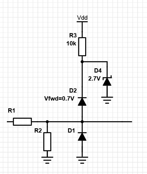
- TVS optional directly on the input (not drawn).
- Vdd is some known high voltage you've got access to, like 24VDC.
- R1 is some high ohm current limiter >10k.
- R2 optional if you need voltage divider
- If some high voltage is applied then you lose 0.7V across D2 and the rest across the zener. You end up with ~3.4V that you can safely connect directly to a 3V3 MCU etc.

1 comment thread