Comments on Via on pad: acceptable or not?
Parent
Via on pad: acceptable or not?
I am designing a PCB with somewhat limited space. To save space, I am placing some vias on component pads. However, I am not sure if this is a good practice in PCB design. As far as I understand, there are certain pros and cons for such designs.
Pros
- Lower impedance for circuits where this matters (RF).
- Saves space on the PCB.
Cons
- Wicks solder away if via is not plugged, affects reflow.
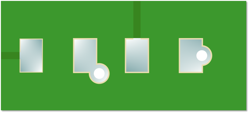
My layout contains vias that are directly placed on pads or at least intersect them (see example below, courtesy of Eurocircuits):
However, it seems like big PCB houses (e.g. Eurocircuits) will offer plugging/filling of vias, eliminating the wicking concern. This makes the production more costly.
If the cost argument is not considered, what is the reason to use or not to use vias on component pads?
Post
This can be OK if you consider and address the consequences carefully. It's something I would only do as a last resort. Usually I try to make sure the hole itself is outside the outline of the pad, and therefore covered with soldermask.
The major problem I see is the via making a thermal connection and slowing down the temperature rise of the pad. This can lead to "tombstoning".
Tombstoning is when one pad of a small 2-pad part heats up before the other so that one has molten solder on it while the other still has unmolten solder paste. The surface tension of molten solder is much higher than that of paste. The high surface tension on one end of the part can cause it to lever up, making it stand vertically on one pad and no longer touching the other. That's why it's called "tombstoning". The part sticks up, like a tombstone does from the ground.
For tombstoning to work, the part has to be small. The part acts like a lever. When the lever is too long, the force to lift the part off the far pad is higher than the surface tension can provide. Generally 0805 are safe from tombstoning, but anything smaller than that is susceptible. At 0603 you have to consider it. Tombstoning can happen readily at 0402 size.
The other thing to worry about is the surface tension of the molten solder pulling the part off-center when the solder on all the pads is melted. This can largely be countered by making sure the solder mask openings are the same for all the pads. You can have more metal leading off some pads than others, but if the solder mask openings are the same there won't be any differential pull from the surface tension.
So, when possible, put the hole of the via far enough away from the pad so that it is covered by solder mask. Only put holes abutting pads when the parts are large enough or have enough pads to prevent tombstoning.
In some cases when you're really space-constrained, put the via in the middle of the pad. Some solder will go down the via, but of course the pad and pin of the part will wick solder too. There should be enough left to allow for a firm connection. However, this is something you should discuss with your assembly house. They know their process better than you do. Tell them what you want to do, and see what they think. If you're not using a lot of small (< 0805) parts, maybe they'll apply a little thicker layer of solder paste. Again, though, this is something where you let them tell you what to do to work well with their process.
1 comment thread

1 comment thread