How do I calculate and manipulate the inductance and capacitance of outputs to a connector on a PCB?
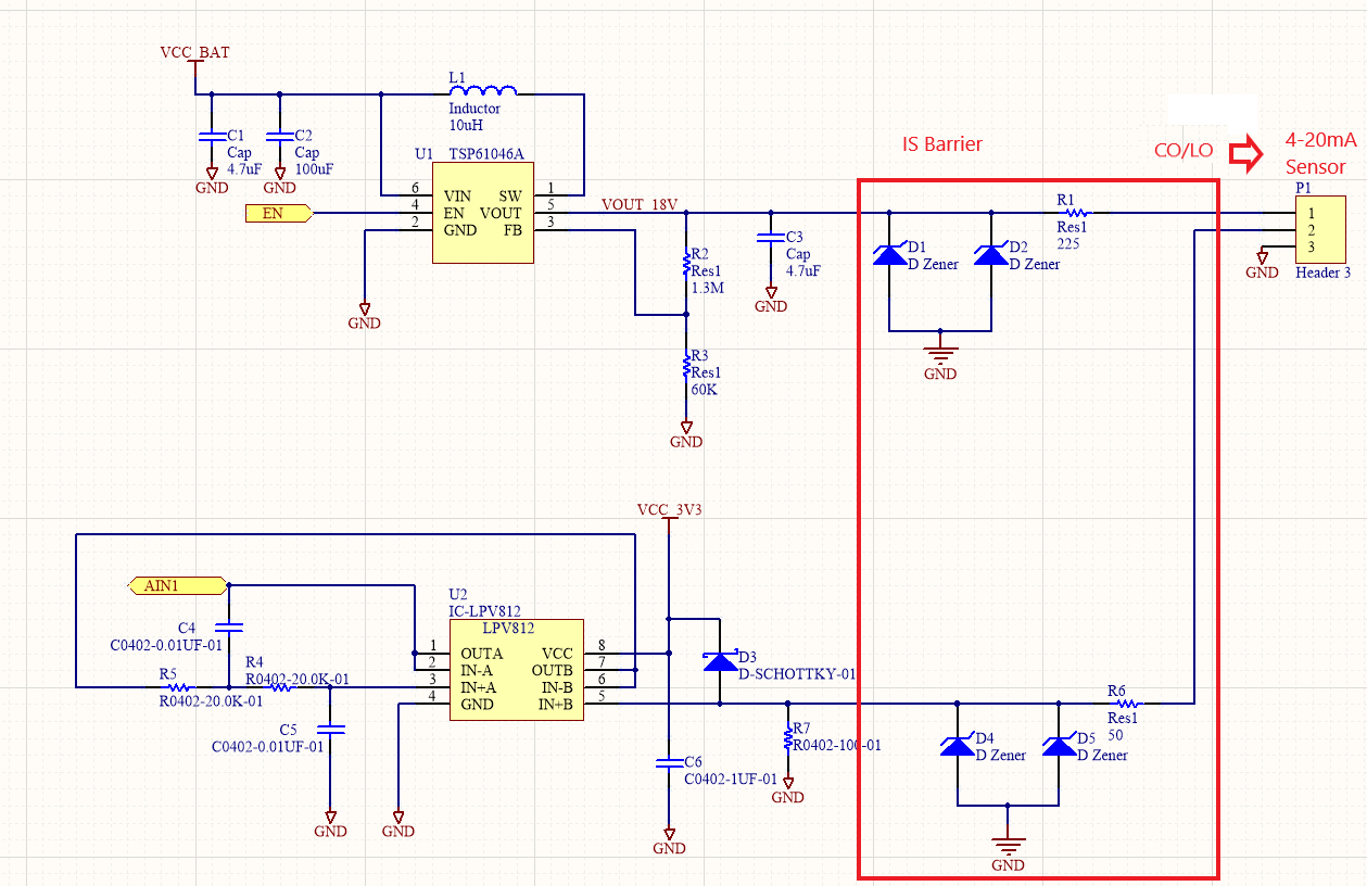
I am designing a PCB that has to have class 1 div 1 associated apparatus (only the outputs to the sensor) certification. Essentially, I am using a boost converter to convert the voltage from a lithium battery of 3.9V to 18V to power a 4-20mA sensor in a hazardous zone, while the main product will be in a safer zone with a class 1 div 2 cert.
I know there could be extra components, such as fuses/diode return; however, it isn't the focus of my question and have simplified the schematic a little bit to focus on the concept I am trying to understand:
The rules for total effective inductance and capacitance can be seen here:
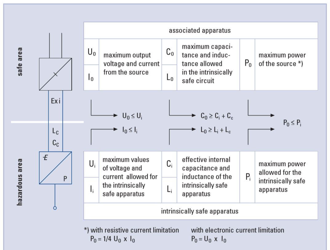
I can get the inductance and capacitance of the sensor + cable (Li+Lc/Ci+Cc) from the manufacturer of the intrinsically safe sensor, but how do I calculate the inductance and capacitance out from the barrier to make sure it is less than the sensor values? The Co and Lo also have to abide by rules to limit the maximum energy allowed in the hazardous area.
The examples I have seen with a similar schematic end up with less than 1uF of capacitance and 2-4mH of inductance for Co and Lo. This seems odd to me when there is only a 10uH inductor and an over abundance of capacitance at 4.7uH on the output of the boost converter. From my understanding, the L and C from the traces will be very minimal in comparison to these numbers.
I do not have a PCB laid out, because I am trying to understand the methodologies and standards first. I understand that means these things can't be completely calculated yet. I'm not asking for someone to design something for me or do calculations for me; I'm just wanting to understand the methodologies behind this question to better understand the concept to use in all of my engineering moving forward.
How do I calculate the theoretical inductance and capacitance at an output? Are there tricks to increasing inductance and decreasing capacitance through the way the board is laid out, or adding components for the specific purpose of manipulating those values?
2 answers
How do I calculate the inductance and capacitance out from the barrier to make sure it is less than the sensor values?
The output capacitance and inductance from your zener barrier is irrelevant - you design the barrier components (fuse, zeners and output resistor) to limit the short circuit current and limit the open circuit voltage. Once designed, the barrier is a zener limited voltage source in series with an infallible resistor. It does not store energy and it does not have any capacitance or inductance.
Then, using graphs for the gas group your unit is to be installed in, you see if there might be a spark energy that can ignite a gas should the sensor have too much inductance or capacitance (when connected to the barrier).
In other words, the barrier buffers (fuse, zeners and resistor) your switching converter to intrinsically safe output levels. But, it's only intrinsically safe if what you hang on the output (the sensor) is permitted i.e. less than the maximum allowable capacitance and inductance.
I'm just wanting to understand the methodologies behind this question to better understand the concept to use in all of my engineering moving forward.
It seems you my be a little inexperienced in this area but it should all become clear when you look in the appropriate standards for intrinsically safety. Your zener barrier maximum output voltage dictates the maximum capacitance that your sensor (and its wiring) can have AND, your zener barrier maximum short circuit current dictates the maximum inductance that your sensor (and its wiring) can have.
It's not completely clear, but it seems you are asking about a circuit in a class 1 div 2 location that will drive another circuit in a class 1 div 1 location.
The point of the IS barrier is to present a Thevenin source. In other words, the two important criteria are the open circuit voltage and short circuit current. Since it seems you are connecting to a previously-certified sensor in the C1 Div1 zone, you need to make sure your barrier provides enough voltage/current, but not more than the sensor is rated for. You have to look at the "entity parameters" of the sensor carefully, and make sure they are not exceeded. Of course for your own purposes, you also have to make sure that the sensor gets enough voltage/current to operate properly.
Since your circuit is still in a hazardous location, you have to look up what exactly the limits are. C1 D2 is less stringent than C1 D1, but there are still limits. Also note that there isn't a single set of limits. There are different sets of limits, depending on the hazardous gas that could be present. For example, the limits are tighter for hydrogen and acetylene than for gasoline vapors.
Once you decide what gas you need to be safe against, there are still various interacting limits. Usually you can derive pessimistic limits that are some maximum inductance and some maximum capacitance, at a voltage level you are guaranteed not to exceed. It's easier if you can live with these. If not, you have to look carefully at series resistance and the like, but that can make your certification process longer and more expensive. This is where you have to read whatever standard you want to claim compliance with very carefully. Actually, you always have to read the standard carefully, but it's easier if you can stick below the "easy" limits.
One issue you may run into is proving that your 18 V will not exceed 18 V, regardless of certain failures. You probably can't. Put another way, the max voltage you use to decide the max capacitance and inductance, isn't your nominal voltage, but something higher you can show won't be exceeded even with some failures. Then there is also derating of parts. For example, those zeners will have some rating, but for IS compliance purposes, their clamping voltage will be higher than that.
In the end, a 18 V supply might be looked at as a 24 V supply worst case, for example. The maximum capacitance and inductance allowed in the circuit will then be a function of the 24 V figure.
It gets complicated. If you've never done this before, I suggest you get a consultant that has experience in this area to guide you and look over your design this first time. Otherwise, you'll probably waste more than the consulting fee going back and forth with the certification agency until you get something they are willing to certify, but that still meets your needs.

1 comment thread