Post History
I am designing a PCB that has to have class 1 div 1 associated apparatus (only the outputs to the sensor) certification. Essentially, I am using a boost converter to convert the voltage from a lith...
#2: Post edited
by
 Lorenzo Donati
·
2023-08-09T21:26:51Z (almost 2 years ago)
Lorenzo Donati
·
2023-08-09T21:26:51Z (almost 2 years ago)
Retagged.
#1: Initial revision
by
 Hawk2020
·
2020-07-07T23:48:23Z (almost 5 years ago)
Hawk2020
·
2020-07-07T23:48:23Z (almost 5 years ago)
I am designing a PCB that has to have class 1 div 1 associated apparatus (only the outputs to the sensor) certification. Essentially, I am using a boost converter to convert the voltage from a lithium battery of 3.9V to 18V to power a 4-20mA sensor in a hazardous zone, while the main product will be in a safer zone with a class 1 div 2 cert. I know there could be extra components, such as fuses/diode return; however, it isn't the focus of my question and have simplified the schematic a little bit to focus on the concept I am trying to understand: 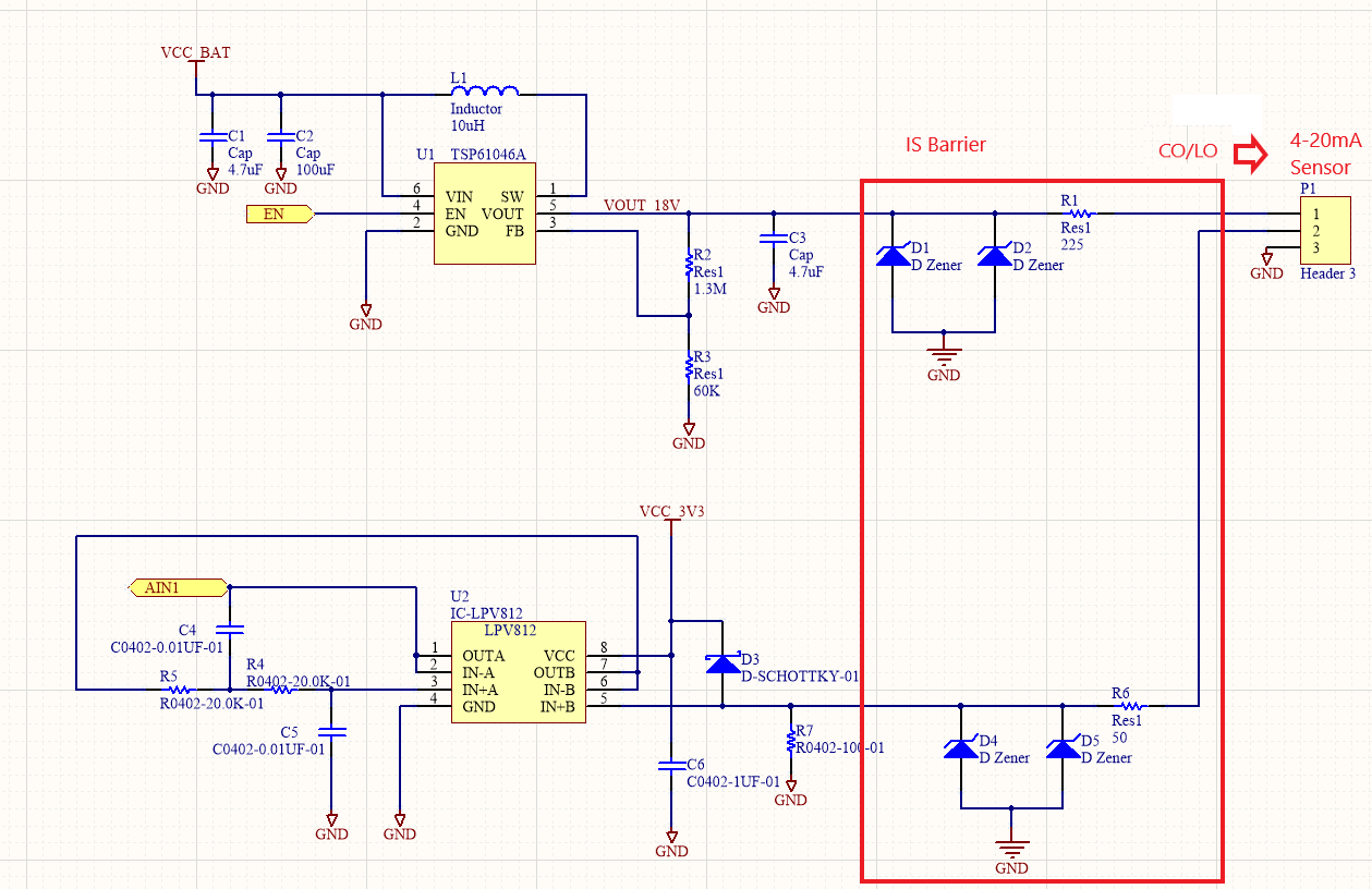 The rules for total effective inductance and capacitance can be seen here: 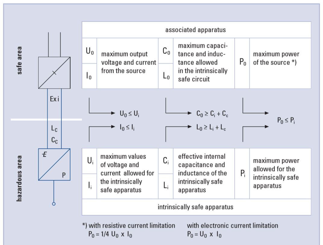 I can get the inductance and capacitance of the sensor + cable (Li+Lc/Ci+Cc) from the manufacturer of the intrinsically safe sensor, but how do I calculate the inductance and capacitance out from the barrier to make sure it is less than the sensor values? The Co and Lo also have to abide by rules to limit the maximum energy allowed in the hazardous area. The examples I have seen with a similar schematic end up with less than 1uF of capacitance and 2-4mH of inductance for Co and Lo. This seems odd to me when there is only a 10uH inductor and an over abundance of capacitance at 4.7uH on the output of the boost converter. From my understanding, the L and C from the traces will be very minimal in comparison to these numbers. I do not have a PCB laid out, because I am trying to understand the methodologies and standards first. I understand that means these things can't be completely calculated yet. I'm not asking for someone to design something for me or do calculations for me; I'm just wanting to understand the methodologies behind this question to better understand the concept to use in all of my engineering moving forward. How do I calculate the theoretical inductance and capacitance at an output? Are there tricks to increasing inductance and decreasing capacitance through the way the board is laid out, or adding components for the specific purpose of manipulating those values?