Amplifier compensation with added resistor across opamp input terminals
This application note from Linear Technology discusses oscillations in opamp circuits and some compensation schemes. One method discussed for reducing phase shifts in the loop gain due to the RC network formed by the feedback network and the opamp input capacitance is shown below for a non-inverting configuration, in which a resistor $R_{IN}$ is added between the opamp input terminals:
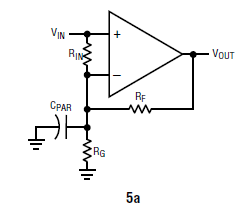
The added resistor $R_{IN}$ reduces the resistance of the divider network as seen by the opamp terminal (assuming a low-source resistance at Vin), pushing the pole formed by the input capacitance and the feedback resistance to higher frequency. This part is easy to understand.
I am looking for help understanding the statement that I have highlighted in the paragraph below that explains the circuit in the app note:
This feedback network appears to be a combination of series and shunt feedback on the input side. I am unclear about how to analyze this circuit from a feedback perspective to understand the highlighted statement.
If you can help point me in the right direction, you can assume an understanding of feedback analysis of common topologies such as inverting and non-inverting configurations. If a detailed explanation is a bit cumbersome, intuitive discussion would be helpful too.
1 answer
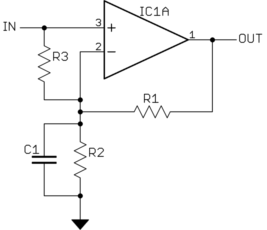
Here is the circuit in question, with the component designators changed to make them easier to write:
To understand this circuit, try building it up in pieces.
First, let's only include R1 and R2. The circuit is then a basic non-inverting amplifier with a gain of (R1 + R2)/R2.
Now let's add C1. The bottom half of the feedback divider is now R2//C1. At low frequencies, C1 is large compared to R2, so the parallel combination is still R2, as it was before. The rolloff frequency is when the impedance magnitudes of C1 and R2 are the same, which happens at f = 1/(2π R2 C1). In a Bode plot, the gain would be flat from DC, then start to go up by 20 dB/decade at the roloff frequency.
With an ideal opamp, this would go up forever. However, real opamps have finite gain×bandwith products. Once the gain gets to be a significant fraction of the gain×bandwidth product, the simple gain equation above becomes invalid, and various unpredictable non-ideal characteristics of the opamp start to matter. We'll assume in the rest of this analysis that we're sticking to frequencies where the ideal approximation of the opamp is still reasonable.
Now let's add R3. Note that due to the feedback (and staying within the usable frequency range as noted above), the negative input of the opamp is driven to IN. Connecting a resistor from there to IN still ends up driving the negative input to the same voltage, but at a lower impedance. This raises the frequency at which C1 starts to become significant. Since C1 starts attenuating the feedback signal at a higher frequency, the bandwidth of the feedback signal becomes higher. Since the overall function is the inverse of the feedback, the overall bandwidth is reduced.
As for the offset voltage, we can get rid of C1 since the offset can be analyzed nicely at DC where C1 has no effect anyway.
With a perfect opamp, R3 shouldn't matter since the voltage across it should always be 0. However, let's imagine the opamp has a 1 mV offset so that it ends up controlling the output such that the negative input stays 1 mV below IN. Now some current will flow thru R3 from In to the negative input node. The current thru R2 is still the same, so this additional R3 current must NOT be coming thru R1. That means the voltage across R1 is lower, and therefore the output voltage is lower than without R3. The net effect of adding R3 is that the input offset voltage of the opamp has a greater effect on the output.

0 comment threads