Post History
#20: Post edited
by
 Lorenzo Donati
·
2023-08-09T19:04:12Z (almost 2 years ago)
Lorenzo Donati
·
2023-08-09T19:04:12Z (almost 2 years ago)
Retagged.
#19: Post edited
by
 Circuit fantasist
·
2022-09-23T19:04:19Z (over 2 years ago)
Circuit fantasist
·
2022-09-23T19:04:19Z (over 2 years ago)
Minor edit
- Goals and objectives
- -------------------------
- **Motivation.** Having shown how a [1-transistor circuit](https://electrical.codidact.com/articles/278933) can be invented, now I will demonstrate how we can invent another more complex 2-transistor circuit. As before, my goals are two - _specific_ (the very 2-transistor circuit) and _general_ (the technology of invention). With my inventor's story, I just want to encourage circuit beginners to be creative by showing them another possible path to invention.
- **Background.** My story is based on three circuit concepts:
- * _voltage divider_ acting as a _reference voltage source_
- * BJT acting as a _comparator_ and _switch_
- * LED acting as a _voltage stabilizer_ and _diode switch_ (_current steering_)
- They are known separately... but the way they are combined here gives an inventive solution.
- **History.** This idea came to me in the early 80's when, in addition to an electronics hobbyist, I was an amateur photographer. I wanted to make a _flash light meter_ with an LED indication for my new camera.
- In [this circuit](https://electrical.codidact.com/uploads/Ky66QamLX19NTN8CKxCnExUF), I converted the light to voltage by an op-amp circuit. Then, I memorize the voltage pulse by something like a _sample & hold_ circuit. Finally, I indicated the voltage by two LEDs connected in the negative feedabck loop to show when the light (voltage) was above or below the desired level. But I wanted to have a third (middle) LED, which would light up when the level was desired. Thus, the LED light would crossfade and an analog indicator would be obtained.
- The problem was how to make the middle diode go out when one of the two end diodes started to light up. In other similar circuits, an additional transistor was used for this purpose... but I did not like it.
- And then I accidentally saw in a book this trick of connecting two LEDs with different threshold voltages in parallel... and immediately applied it in my circuit. I found it very interesting; I abandoned photography and started experimenting with various circuits of LED voltage indicators. Finally, I obtained two [patents](https://electrical.codidact.com/uploads/J5GYukv2WT3MLq4TpsJURsDM)...
- **Presentation.** Below I have reproduced, step by step, the path I have taken in the form of an imaginary _inventive scenario_. This is a good example of how an inventor thinks when inventing.
- I have illustrated each step by a conceptual circuit diagram where the invisible electrical quantities are visualized. The voltages are represented by vertical segments (_voltage bars_) with proportional height in red. They are summed (subtracted) geometrically according to KVL. This clearly shows the relationship between voltages. The set of voltage bars on the circuit diagram can be considered as a snapshot of the voltage relief. For the purposes of this qualitative presentation, numerical values are not given because they are not significant here.
- The current paths are shown by closed lines (_current loops_) in green that start from the positive terminal of the power supply and end at its negative terminal. The current magnitude can be shown by the line thickness but here, for simplicity, this technique is not used.
- In the final Step 7, I have drawn the circuit diagram in its conventional compact form - no voltage bars, no current loops, no colors, no unusually situated elements... So you have a choice - if you do not like step-by-step invention and visualization, you can jump directly to Fig. 7.
- “Inventing” the circuit
- ----------------------------
- **1. Obtaining the threshold voltage VTR.** To make a threshold voltage circuit, first at all, we need to set the threshold (reference) voltage. The simplest way to obtain it is by the ubiquitous _voltage divider_. Let's initially choose VREF = VCC/2 (or zero, in the case of a dual power supply). This means to connect two equal resistors R1 = R2 in series - Fig. 1. The voltage drops across them are equal as well - VR1 = VR2, and we take the lower grounded voltage in point A.
- 
- Fig. 1. "Producing" a reference voltage by a voltage divider R1-R2 and input voltage VIN by a potentiometer P.
- In a similar way - by the potentiometer P, we can emulate the previous stage producing the input voltage VIN (the light-to-voltage converter from my story above). Note the potentiometer and the power supply do not belong to the invented circuit that is outlined in yellow.
- **2. Inserting the first (middle) diode.** Now we have to supply the first (middle) LED D1. Let's insert it between the two resistors - Fig. 2, to "lift" its voltage drop VD1 by the threshold voltage VIN/2. By choosing the sum of their resistance, we set the desired current through D1.
- 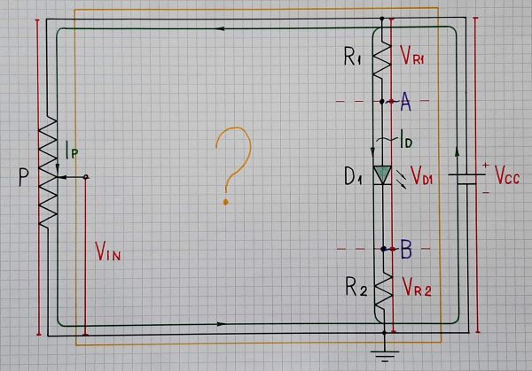
- Fig. 2. Including the first (middle) LED D1.
- Now we have two slightly differing reference voltages - below D1 (point B) and above D1 (point A).
- **3. Building the upper comparator.** Now, we have to _compare_ the input voltage with the reference voltages and _connect_ the according end LED depending on the difference. Both can be implemented by a _bipolar junction transistor_.
- Let's begin with the upper comparator. We can make it by an NPN transistor (T1) by connecting its emitter to the lower reference voltage (point B) and its base to the input voltage (through a resistor RB) - Fig. 3. But it should switch LED D3; so let's insert D3 in the emitter. Its forward voltage and T1 base-emitter voltage VBE will be added to the lower reference voltage VR2 thus forming the high threshold voltage.
- 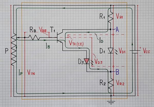
- Fig. 3. Building the upper comparator
- When the input voltage exceeds the high threshold, T1 begins conducting and D3 will begin lighting up. But D1 should start to go out. How do we do it?
- Here chance helps us - it turns out that D1 goes out on its own. But why?
- D1 is a green LED with forward voltage VD1 = 2.5 V and D3 is a red LED with forward voltage VD3 = 1.8 V. They are connected in parallel; so the current is diverted (steered) from D1 to D3... and they cross fade.
- So, our chance was that we connected, by accident, an LED with lower forward voltage (red) in parallel to an LED with higher voltage (green). If we had done the opposite, the trick would not have worked...
- **4. Building the lower comparator.** Now we should use a PNP transistor (T2) by connecting its emitter to the higher reference voltage (point A) and its base to the input voltage - Fig. 4. It should switch LED D2; so we insert D2 in the emitter. Its forward voltage and T2 base-emitter voltage VBE will be subtracted from the higher reference voltage (Vcc - VR1) thus forming the low threshold voltage.
- 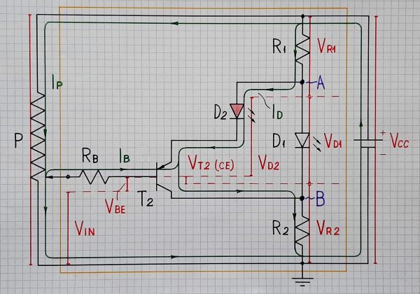
- Fig. 4. Building the lower comparator.
- Now, when the input voltage drops below the low threshold, T2 begins connecting D2 in parallel to D1. The current is steered from D1 to D2 and the LEDs cross fade.
- **5. Combining the two comparators.** Now it remains only to combine the two comparators in one _window comparator_ - Fig. 5.
- 
- Fig. 5. Combining the two comparators in one.
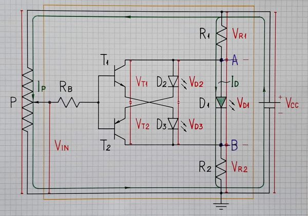
- **6. Simplifying the circuit.** But we do not like these cross-connections. What happens if we join them to make the circuit tidier? Let's try - Fig. 6.
- 
- Fig. 6. The circuit can be simplified by joining the emitters.
- The result is really a more beautiful circuit. All that remains is it to work:) And it really works... and even better! Let's see why.
- In addition to the previous version, now when the transistor T1/T2 connects the end LED D3/D2 in parallel to the middle LED D1, it shunts the other end LED D2/D3 and reliably turns it off.
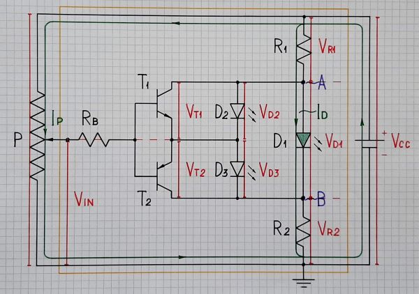
- **7. Usually drawn circuit.** Finally, let's remove all these visual aids and draw the circuit in the conventional way - Fig. 7.
- 
- Fig. 7. The circuit is drawn without visualized electrical quantities (a dual-supplied version).
- How neat it is... small, beautiful and symmetrical!
- Properties
- ----------
- Look at the central part of the circuit including the two transistors T1, T2 and three LEDs D1-D3. This structure has unique properties:
- **Constant voltage.** Regardless of the state in which it is (switched on D1, D2 or D3... or an intermediate state), the voltage drop across it (between points A and B) changes slightly. The whole structure behaves like one diode (LED).
- **Constant current.** Also, regardless of the state, the whole current through this structure changes slightly. It only diverts between diodes (as they say, it is "steered" between LEDs). This phenomenon is known as _current steering_ and is usually associated with the differential (long-tailed) pair.
- **Mobility.** Figuratively speaking, this structure is "stretched" through two resistors (pull-up R1 and pull-down R2) between the supply rails. If we change simultaneously and in opposite directions their resistances, we can "move" this "diode" up to V+ and down to ground or V- without changing the voltage across it (VA - VB) and the current through it.
- **Bridge circuit.** If the voltage indicator is driven by a potentiometer (as it is here), the whole circuit (including the potentiometer) can be considered as a Wheatstone bridge with a zero indicator. It consists of the two potentiometer half resistances and resistors R1 and R2. The central part serves as the _zero voltage indicator_.
- Improvements
- ------------
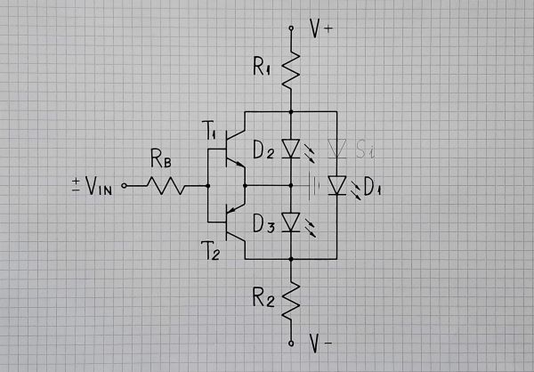
- **Dual-supplied version.** In addition, we can draw its dual-supplied version - Fig. 7 above.
- **Grounded version.** If this is a _zero voltage indicator_, we can ground the common emitter point (shown in light gray in Fig. 7). Thus the emitter voltages will be firmly fixed.
- **Direct control.** The circuit can be further simplified by removing RB (when the emitters are not grounded). This will make it even more sensitive. There is no danger of damage to the transistors because resistors R1 and R2 limit the base currents. Only the circuit input resistance will be lower.
- **Identical LEDs.** The circuit can be implemented by identical LEDs (with equal VF). In this case, we can increase D1 forward voltage by inserting an ordinary Si diode in series.
- **Narrow dead zone.** The width of the "dead zone" is 2VBE. It can be narrowed by applying a bias voltage as @TonyStewart suggests in his attractive [FS simulation](http://www.falstad.com/circuit/circuitjs.html?ctz=CQAgDOB0YzCsICMjoA4BsB2ATNzjs4BOVA9EAFgGYkILsAoAFxEPOzFRCrAtc-BIQAWhSYi6CvRIVM6bETh9hYaGEw8cPbIkUk4qIrTDNWcdjm69WliKKhh0iR4nO64CzkTAIVkdAGImGBUGh5EiBjkziYA7lZ8utjc6FxJ3AzxVKmsqFw8fNh5SJkJrNh8BawUECYATuWFlriVHIK4sAwNLfxcPQRcEB0wDAAmjdVDFTbJyaMApgBmAIYArgA2TKU9VG1Vu7Xb0wNlJyYAShMHVx6CdHYItVBwYxMcfdMVQyALKxtbAHMQOgBF8QMRZjVwF1TkVTkRklNVLAUaiQqVsn1ijUhsULsCBNcQflbk8ocJHndIC9LsSkHC6RI7pQIJTatTSuhzJNgdy2ND4kpCgIhTzGFkcukcUgEdCGnT0gq4Ui1GjUVQYXSilw6dcVWq0Rr4lqoVz2FC4gS+qbQdzEJzQdMTRB7SxRXhklrbCJEFBMKQ4HAqM5UAZxJIRKpzI4uWBsLsqEQaoRjKZ3QItQIXT7IEnUv6KKhxHACDwjH5owE4HGE0m4wgYgxEPJedFZWa3j8lmtNsJ1vNxr6nsjGM3PXzuR3tawu39e-3xtn2XGHVidXzivbjXzTXzppaFe27bKD5vZcFErLxcDitOL7k0gxLlUTlUmWTWcyozD3VCS5CnhieokDkMVPgtYxLV-VkpBmVgmxbTEZWSJCwTmbt-j7AchGHaBR0QnIwVQ29Zx7JgsMHHCHEYKg+F+MiKIAHQAZwAdUEFBsHmURszgfxoTHFkXVlaVp3QudyIXFj2N9WTqJhKpp32Np9QNFEjTKIjCKhe1LiCcgI0QWCI2zC1cxTXCXiyawiJs7kTCBRSoTEi1tj5R1hT6NyLFmT5mlKf8eUCwzSn0nkwpC+IIr4YK+FPNIjzbRFOVvYopzxBgahoZBkgoZtuFQPhCzJKgAH1JFKsBSooINcEq8y4Hq2BEFKlrsGqsqNUE+90nvMTSMwqS2KEOSRwYAB7ArgTiyhaqHVV5rARAqGIJx6CMwgMAqIxviofIJu4IwTNm3ZFpgRbltWjaNohXgZpQowNUm00Zpq06HHOhxm0TWjdCrCpCt2doWQySa8GmwQ3p0D6lq+6gKCwDg8AoIh-W8bKZ3Bp7cghug5phi74cRuNMBR1A9tkIRZn2yalFx7h8AUcFqIbGc6Y1PbKBodlWYAWWWAAPFiADVxs2ZYAXmBggA):
- 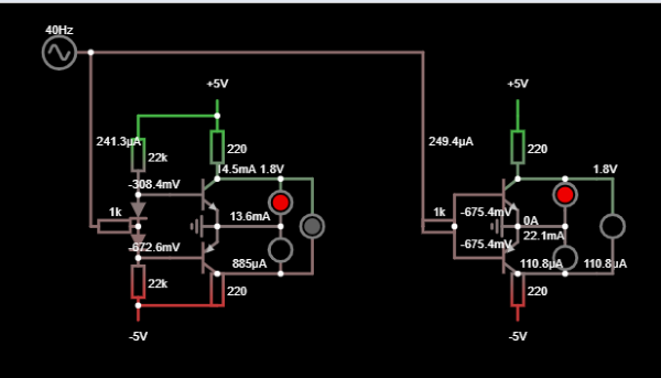
- Fig. 8. LED indicator - simulation (by @TonyStewart)
- The bias voltage is created across diodes connected in parallel to base-emitter junctions. This is a well-known bias technique widely used in output stages of power amplifiers.
- **Wide dead zone.** Conversely, we can expand the "dead zone" (if necessary) by inserting diodes *in series* to the base-emitter junctions.
- See also
- --------
[A similar Wikibooks story](https://en.m.wikibooks.org/wiki/Circuit_Idea/Group_57a#Lab_1_Building_LED_Voltage_Indicator_using_transistor_switches) (written by my students in 2010]
- Goals and objectives
- -------------------------
- **Motivation.** Having shown how a [1-transistor circuit](https://electrical.codidact.com/articles/278933) can be invented, now I will demonstrate how we can invent another more complex 2-transistor circuit. As before, my goals are two - _specific_ (the very 2-transistor circuit) and _general_ (the technology of invention). With my inventor's story, I just want to encourage circuit beginners to be creative by showing them another possible path to invention.
- **Background.** My story is based on three circuit concepts:
- * _voltage divider_ acting as a _reference voltage source_
- * BJT acting as a _comparator_ and _switch_
- * LED acting as a _voltage stabilizer_ and _diode switch_ (_current steering_)
- They are known separately... but the way they are combined here gives an inventive solution.
- **History.** This idea came to me in the early 80's when, in addition to an electronics hobbyist, I was an amateur photographer. I wanted to make a _flash light meter_ with an LED indication for my new camera.
- In [this circuit](https://electrical.codidact.com/uploads/Ky66QamLX19NTN8CKxCnExUF), I converted the light to voltage by an op-amp circuit. Then, I memorize the voltage pulse by something like a _sample & hold_ circuit. Finally, I indicated the voltage by two LEDs connected in the negative feedabck loop to show when the light (voltage) was above or below the desired level. But I wanted to have a third (middle) LED, which would light up when the level was desired. Thus, the LED light would crossfade and an analog indicator would be obtained.
- The problem was how to make the middle diode go out when one of the two end diodes started to light up. In other similar circuits, an additional transistor was used for this purpose... but I did not like it.
- And then I accidentally saw in a book this trick of connecting two LEDs with different threshold voltages in parallel... and immediately applied it in my circuit. I found it very interesting; I abandoned photography and started experimenting with various circuits of LED voltage indicators. Finally, I obtained two [patents](https://electrical.codidact.com/uploads/J5GYukv2WT3MLq4TpsJURsDM)...
- **Presentation.** Below I have reproduced, step by step, the path I have taken in the form of an imaginary _inventive scenario_. This is a good example of how an inventor thinks when inventing.
- I have illustrated each step by a conceptual circuit diagram where the invisible electrical quantities are visualized. The voltages are represented by vertical segments (_voltage bars_) with proportional height in red. They are summed (subtracted) geometrically according to KVL. This clearly shows the relationship between voltages. The set of voltage bars on the circuit diagram can be considered as a snapshot of the voltage relief. For the purposes of this qualitative presentation, numerical values are not given because they are not significant here.
- The current paths are shown by closed lines (_current loops_) in green that start from the positive terminal of the power supply and end at its negative terminal. The current magnitude can be shown by the line thickness but here, for simplicity, this technique is not used.
- In the final Step 7, I have drawn the circuit diagram in its conventional compact form - no voltage bars, no current loops, no colors, no unusually situated elements... So you have a choice - if you do not like step-by-step invention and visualization, you can jump directly to Fig. 7.
- “Inventing” the circuit
- ----------------------------
- **1. Obtaining the threshold voltage VTR.** To make a threshold voltage circuit, first at all, we need to set the threshold (reference) voltage. The simplest way to obtain it is by the ubiquitous _voltage divider_. Let's initially choose VREF = VCC/2 (or zero, in the case of a dual power supply). This means to connect two equal resistors R1 = R2 in series - Fig. 1. The voltage drops across them are equal as well - VR1 = VR2, and we take the lower grounded voltage in point A.
- 
- Fig. 1. "Producing" a reference voltage by a voltage divider R1-R2 and input voltage VIN by a potentiometer P.
- In a similar way - by the potentiometer P, we can emulate the previous stage producing the input voltage VIN (the light-to-voltage converter from my story above). Note the potentiometer and the power supply do not belong to the invented circuit that is outlined in yellow.
- **2. Inserting the first (middle) diode.** Now we have to supply the first (middle) LED D1. Let's insert it between the two resistors - Fig. 2, to "lift" its voltage drop VD1 by the threshold voltage VIN/2. By choosing the sum of their resistance, we set the desired current through D1.
- 
- Fig. 2. Including the first (middle) LED D1.
- Now we have two slightly differing reference voltages - below D1 (point B) and above D1 (point A).
- **3. Building the upper comparator.** Now, we have to _compare_ the input voltage with the reference voltages and _connect_ the according end LED depending on the difference. Both can be implemented by a _bipolar junction transistor_.
- Let's begin with the upper comparator. We can make it by an NPN transistor (T1) by connecting its emitter to the lower reference voltage (point B) and its base to the input voltage (through a resistor RB) - Fig. 3. But it should switch LED D3; so let's insert D3 in the emitter. Its forward voltage and T1 base-emitter voltage VBE will be added to the lower reference voltage VR2 thus forming the high threshold voltage.
- 
- Fig. 3. Building the upper comparator
- When the input voltage exceeds the high threshold, T1 begins conducting and D3 will begin lighting up. But D1 should start to go out. How do we do it?
- Here chance helps us - it turns out that D1 goes out on its own. But why?
- D1 is a green LED with forward voltage VD1 = 2.5 V and D3 is a red LED with forward voltage VD3 = 1.8 V. They are connected in parallel; so the current is diverted (steered) from D1 to D3... and they cross fade.
- So, our chance was that we connected, by accident, an LED with lower forward voltage (red) in parallel to an LED with higher voltage (green). If we had done the opposite, the trick would not have worked...
- **4. Building the lower comparator.** Now we should use a PNP transistor (T2) by connecting its emitter to the higher reference voltage (point A) and its base to the input voltage - Fig. 4. It should switch LED D2; so we insert D2 in the emitter. Its forward voltage and T2 base-emitter voltage VBE will be subtracted from the higher reference voltage (Vcc - VR1) thus forming the low threshold voltage.
- 
- Fig. 4. Building the lower comparator.
- Now, when the input voltage drops below the low threshold, T2 begins connecting D2 in parallel to D1. The current is steered from D1 to D2 and the LEDs cross fade.
- **5. Combining the two comparators.** Now it remains only to combine the two comparators in one _window comparator_ - Fig. 5.
- 
- Fig. 5. Combining the two comparators in one.
- **6. Simplifying the circuit.** But we do not like these cross-connections. What happens if we join them to make the circuit tidier? Let's try - Fig. 6.
- 
- Fig. 6. The circuit can be simplified by joining the emitters.
- The result is really a more beautiful circuit. All that remains is it to work:) And it really works... and even better! Let's see why.
- In addition to the previous version, now when the transistor T1/T2 connects the end LED D3/D2 in parallel to the middle LED D1, it shunts the other end LED D2/D3 and reliably turns it off.
- **7. Usually drawn circuit.** Finally, let's remove all these visual aids and draw the circuit in the conventional way - Fig. 7.
- 
- Fig. 7. The circuit is drawn without visualized electrical quantities (a dual-supplied version).
- How neat it is... small, beautiful and symmetrical!
- Properties
- ----------
- Look at the central part of the circuit including the two transistors T1, T2 and three LEDs D1-D3. This structure has unique properties:
- **Constant voltage.** Regardless of the state in which it is (switched on D1, D2 or D3... or an intermediate state), the voltage drop across it (between points A and B) changes slightly. The whole structure behaves like one diode (LED).
- **Constant current.** Also, regardless of the state, the whole current through this structure changes slightly. It only diverts between diodes (as they say, it is "steered" between LEDs). This phenomenon is known as _current steering_ and is usually associated with the differential (long-tailed) pair.
- **Mobility.** Figuratively speaking, this structure is "stretched" through two resistors (pull-up R1 and pull-down R2) between the supply rails. If we change simultaneously and in opposite directions their resistances, we can "move" this "diode" up to V+ and down to ground or V- without changing the voltage across it (VA - VB) and the current through it.
- **Bridge circuit.** If the voltage indicator is driven by a potentiometer (as it is here), the whole circuit (including the potentiometer) can be considered as a Wheatstone bridge with a zero indicator. It consists of the two potentiometer half resistances and resistors R1 and R2. The central part serves as the _zero voltage indicator_.
- Improvements
- ------------
- **Dual-supplied version.** In addition, we can draw its dual-supplied version - Fig. 7 above.
- **Grounded version.** If this is a _zero voltage indicator_, we can ground the common emitter point (shown in light gray in Fig. 7). Thus the emitter voltages will be firmly fixed.
- **Direct control.** The circuit can be further simplified by removing RB (when the emitters are not grounded). This will make it even more sensitive. There is no danger of damage to the transistors because resistors R1 and R2 limit the base currents. Only the circuit input resistance will be lower.
- **Identical LEDs.** The circuit can be implemented by identical LEDs (with equal VF). In this case, we can increase D1 forward voltage by inserting an ordinary Si diode in series.
- **Narrow dead zone.** The width of the "dead zone" is 2VBE. It can be narrowed by applying a bias voltage as @TonyStewart suggests in his attractive [FS simulation](http://www.falstad.com/circuit/circuitjs.html?ctz=CQAgDOB0YzCsICMjoA4BsB2ATNzjs4BOVA9EAFgGYkILsAoAFxEPOzFRCrAtc-BIQAWhSYi6CvRIVM6bETh9hYaGEw8cPbIkUk4qIrTDNWcdjm69WliKKhh0iR4nO64CzkTAIVkdAGImGBUGh5EiBjkziYA7lZ8utjc6FxJ3AzxVKmsqFw8fNh5SJkJrNh8BawUECYATuWFlriVHIK4sAwNLfxcPQRcEB0wDAAmjdVDFTbJyaMApgBmAIYArgA2TKU9VG1Vu7Xb0wNlJyYAShMHVx6CdHYItVBwYxMcfdMVQyALKxtbAHMQOgBF8QMRZjVwF1TkVTkRklNVLAUaiQqVsn1ijUhsULsCBNcQflbk8ocJHndIC9LsSkHC6RI7pQIJTatTSuhzJNgdy2ND4kpCgIhTzGFkcukcUgEdCGnT0gq4Ui1GjUVQYXSilw6dcVWq0Rr4lqoVz2FC4gS+qbQdzEJzQdMTRB7SxRXhklrbCJEFBMKQ4HAqM5UAZxJIRKpzI4uWBsLsqEQaoRjKZ3QItQIXT7IEnUv6KKhxHACDwjH5owE4HGE0m4wgYgxEPJedFZWa3j8lmtNsJ1vNxr6nsjGM3PXzuR3tawu39e-3xtn2XGHVidXzivbjXzTXzppaFe27bKD5vZcFErLxcDitOL7k0gxLlUTlUmWTWcyozD3VCS5CnhieokDkMVPgtYxLV-VkpBmVgmxbTEZWSJCwTmbt-j7AchGHaBR0QnIwVQ29Zx7JgsMHHCHEYKg+F+MiKIAHQAZwAdUEFBsHmURszgfxoTHFkXVlaVp3QudyIXFj2N9WTqJhKpp32Np9QNFEjTKIjCKhe1LiCcgI0QWCI2zC1cxTXCXiyawiJs7kTCBRSoTEi1tj5R1hT6NyLFmT5mlKf8eUCwzSn0nkwpC+IIr4YK+FPNIjzbRFOVvYopzxBgahoZBkgoZtuFQPhCzJKgAH1JFKsBSooINcEq8y4Hq2BEFKlrsGqsqNUE+90nvMTSMwqS2KEOSRwYAB7ArgTiyhaqHVV5rARAqGIJx6CMwgMAqIxviofIJu4IwTNm3ZFpgRbltWjaNohXgZpQowNUm00Zpq06HHOhxm0TWjdCrCpCt2doWQySa8GmwQ3p0D6lq+6gKCwDg8AoIh-W8bKZ3Bp7cghug5phi74cRuNMBR1A9tkIRZn2yalFx7h8AUcFqIbGc6Y1PbKBodlWYAWWWAAPFiADVxs2ZYAXmBggA):
- 
- Fig. 8. LED indicator - simulation (by @TonyStewart)
- The bias voltage is created across diodes connected in parallel to base-emitter junctions. This is a well-known bias technique widely used in output stages of power amplifiers.
- **Wide dead zone.** Conversely, we can expand the "dead zone" (if necessary) by inserting diodes *in series* to the base-emitter junctions.
- See also
- --------
- [A similar Wikibooks story](https://en.m.wikibooks.org/wiki/Circuit_Idea/Group_57a#Lab_1_Building_LED_Voltage_Indicator_using_transistor_switches) (written by my students in 2010)
#18: Post edited
by
Circuit fantasist
·
2022-09-23T17:17:14Z (over 2 years ago)
Minor edit
- Goals and objectives
- -------------------------
- **Motivation.** Having shown how a [1-transistor circuit](https://electrical.codidact.com/articles/278933) can be invented, now I will demonstrate how we can invent another more complex 2-transistor circuit. As before, my goals are two - _specific_ (the very 2-transistor circuit) and _general_ (the technology of invention). With my inventor's story, I just want to encourage circuit beginners to be creative by showing them another possible path to invention.
- **Background.** My story is based on three circuit concepts:
- * _voltage divider_ acting as a _reference voltage source_
- * BJT acting as a _comparator_ and _switch_
- * LED acting as a _voltage stabilizer_ and _diode switch_ (_current steering_)
- They are known separately... but the way they are combined here gives an inventive solution.
- **History.** This idea came to me in the early 80's when, in addition to an electronics hobbyist, I was an amateur photographer. I wanted to make a _flash light meter_ with an LED indication for my new camera.
- In [this circuit](https://electrical.codidact.com/uploads/Ky66QamLX19NTN8CKxCnExUF), I converted the light to voltage by an op-amp circuit. Then, I memorize the voltage pulse by something like a _sample & hold_ circuit. Finally, I indicated the voltage by two LEDs connected in the negative feedabck loop to show when the light (voltage) was above or below the desired level. But I wanted to have a third (middle) LED, which would light up when the level was desired. Thus, the LED light would crossfade and an analog indicator would be obtained.
- The problem was how to make the middle diode go out when one of the two end diodes started to light up. In other similar circuits, an additional transistor was used for this purpose... but I did not like it.
- And then I accidentally saw in a book this trick of connecting two LEDs with different threshold voltages in parallel... and immediately applied it in my circuit. I found it very interesting; I abandoned photography and started experimenting with various circuits of LED voltage indicators. Finally, I obtained two [patents](https://electrical.codidact.com/uploads/J5GYukv2WT3MLq4TpsJURsDM)...
- **Presentation.** Below I have reproduced, step by step, the path I have taken in the form of an imaginary _inventive scenario_. This is a good example of how an inventor thinks when inventing.
- I have illustrated each step by a conceptual circuit diagram where the invisible electrical quantities are visualized. The voltages are represented by vertical segments (_voltage bars_) with proportional height in red. They are summed (subtracted) geometrically according to KVL. This clearly shows the relationship between voltages. The set of voltage bars on the circuit diagram can be considered as a snapshot of the voltage relief. For the purposes of this qualitative presentation, numerical values are not given because they are not significant here.
- The current paths are shown by closed lines (_current loops_) in green that start from the positive terminal of the power supply and end at its negative terminal. The current magnitude can be shown by the line thickness but here, for simplicity, this technique is not used.
- In the final Step 7, I have drawn the circuit diagram in its conventional compact form - no voltage bars, no current loops, no colors, no unusually situated elements... So you have a choice - if you do not like step-by-step invention and visualization, you can jump directly to Fig. 7.
- “Inventing” the circuit
- ----------------------------
- **1. Obtaining the threshold voltage VTR.** To make a threshold voltage circuit, first at all, we need to set the threshold (reference) voltage. The simplest way to obtain it is by the ubiquitous _voltage divider_. Let's initially choose VREF = VCC/2 (or zero, in the case of a dual power supply). This means to connect two equal resistors R1 = R2 in series - Fig. 1. The voltage drops across them are equal as well - VR1 = VR2, and we take the lower grounded voltage in point A.
- 
- Fig. 1. "Producing" a reference voltage by a voltage divider R1-R2 and input voltage VIN by a potentiometer P.
- In a similar way - by the potentiometer P, we can emulate the previous stage producing the input voltage VIN (the light-to-voltage converter from my story above). Note the potentiometer and the power supply do not belong to the invented circuit that is outlined in yellow.
- **2. Inserting the first (middle) diode.** Now we have to supply the first (middle) LED D1. Let's insert it between the two resistors - Fig. 2, to "lift" its voltage drop VD1 by the threshold voltage VIN/2. By choosing the sum of their resistance, we set the desired current through D1.
- 
- Fig. 2. Including the first (middle) LED D1.
- Now we have two slightly differing reference voltages - below D1 (point B) and above D1 (point A).
- **3. Building the upper comparator.** Now, we have to _compare_ the input voltage with the reference voltages and _connect_ the according end LED depending on the difference. Both can be implemented by a _bipolar junction transistor_.
- Let's begin with the upper comparator. We can make it by an NPN transistor (T1) by connecting its emitter to the lower reference voltage (point B) and its base to the input voltage (through a resistor RB) - Fig. 3. But it should switch LED D3; so let's insert D3 in the emitter. Its forward voltage and T1 base-emitter voltage VBE will be added to the lower reference voltage VR2 thus forming the high threshold voltage.
- 
- Fig. 3. Building the upper comparator
- When the input voltage exceeds the high threshold, T1 begins conducting and D3 will begin lighting up. But D1 should start to go out. How do we do it?
- Here chance helps us - it turns out that D1 goes out on its own. But why?
- D1 is a green LED with forward voltage VD1 = 2.5 V and D3 is a red LED with forward voltage VD3 = 1.8 V. They are connected in parallel; so the current is diverted (steered) from D1 to D3... and they cross fade.
- So, our chance was that we connected, by accident, an LED with lower forward voltage (red) in parallel to an LED with higher voltage (green). If we had done the opposite, the trick would not have worked...
- **4. Building the lower comparator.** Now we should use a PNP transistor (T2) by connecting its emitter to the higher reference voltage (point A) and its base to the input voltage - Fig. 4. It should switch LED D2; so we insert D2 in the emitter. Its forward voltage and T2 base-emitter voltage VBE will be subtracted from the higher reference voltage (Vcc - VR1) thus forming the low threshold voltage.
- 
- Fig. 4. Building the lower comparator.
- Now, when the input voltage drops below the low threshold, T2 begins connecting D2 in parallel to D1. The current is steered from D1 to D2 and the LEDs cross fade.
- **5. Combining the two comparators.** Now it remains only to combine the two comparators in one _window comparator_ - Fig. 5.
- 
- Fig. 5. Combining the two comparators in one.
- **6. Simplifying the circuit.** But we do not like these cross-connections. What happens if we join them to make the circuit tidier? Let's try - Fig. 6.
- 
- Fig. 6. The circuit can be simplified by joining the emitters.
- The result is really a more beautiful circuit. All that remains is it to work:) And it really works... and even better! Let's see why.
- In addition to the previous version, now when the transistor T1/T2 connects the end LED D3/D2 in parallel to the middle LED D1, it shunts the other end LED D2/D3 and reliably turns it off.
- **7. Usually drawn circuit.** Finally, let's remove all these visual aids and draw the circuit in the conventional way - Fig. 7.
- 
- Fig. 7. The circuit is drawn without visualized electrical quantities (a dual-supplied version).
- How neat it is... small, beautiful and symmetrical!
- Properties
- ----------
- Look at the central part of the circuit including the two transistors T1, T2 and three LEDs D1-D3. This structure has unique properties:
- **Constant voltage.** Regardless of the state in which it is (switched on D1, D2 or D3... or an intermediate state), the voltage drop across it (between points A and B) changes slightly. The whole structure behaves like one diode (LED).
- **Constant current.** Also, regardless of the state, the whole current through this structure changes slightly. It only diverts between diodes (as they say, it is "steered" between LEDs). This phenomenon is known as _current steering_ and is usually associated with the differential (long-tailed) pair.
- **Mobility.** Figuratively speaking, this structure is "stretched" through two resistors (pull-up R1 and pull-down R2) between the supply rails. If we change simultaneously and in opposite directions their resistances, we can "move" this "diode" up to V+ and down to ground or V- without changing the voltage across it (VA - VB) and the current through it.
- **Bridge circuit.** If the voltage indicator is driven by a potentiometer (as it is here), the whole circuit (including the potentiometer) can be considered as a Wheatstone bridge with a zero indicator. It consists of the two potentiometer half resistances and resistors R1 and R2. The central part serves as the _zero voltage indicator_.
- Improvements
- ------------
- **Dual-supplied version.** In addition, we can draw its dual-supplied version - Fig. 7 above.
- **Grounded version.** If this is a _zero voltage indicator_, we can ground the common emitter point (shown in light gray in Fig. 7). Thus the emitter voltages will be firmly fixed.
- **Direct control.** The circuit can be further simplified by removing RB (when the emitters are not grounded). This will make it even more sensitive. There is no danger of damage to the transistors because resistors R1 and R2 limit the base currents. Only the circuit input resistance will be lower.
- **Identical LEDs.** The circuit can be implemented by identical LEDs (with equal VF). In this case, we can increase D1 forward voltage by inserting an ordinary Si diode in series.
- **Narrow dead zone.** The width of the "dead zone" is 2VBE. It can be narrowed by applying a bias voltage as @TonyStewart suggests in his attractive [FS simulation](http://www.falstad.com/circuit/circuitjs.html?ctz=CQAgDOB0YzCsICMjoA4BsB2ATNzjs4BOVA9EAFgGYkILsAoAFxEPOzFRCrAtc-BIQAWhSYi6CvRIVM6bETh9hYaGEw8cPbIkUk4qIrTDNWcdjm69WliKKhh0iR4nO64CzkTAIVkdAGImGBUGh5EiBjkziYA7lZ8utjc6FxJ3AzxVKmsqFw8fNh5SJkJrNh8BawUECYATuWFlriVHIK4sAwNLfxcPQRcEB0wDAAmjdVDFTbJyaMApgBmAIYArgA2TKU9VG1Vu7Xb0wNlJyYAShMHVx6CdHYItVBwYxMcfdMVQyALKxtbAHMQOgBF8QMRZjVwF1TkVTkRklNVLAUaiQqVsn1ijUhsULsCBNcQflbk8ocJHndIC9LsSkHC6RI7pQIJTatTSuhzJNgdy2ND4kpCgIhTzGFkcukcUgEdCGnT0gq4Ui1GjUVQYXSilw6dcVWq0Rr4lqoVz2FC4gS+qbQdzEJzQdMTRB7SxRXhklrbCJEFBMKQ4HAqM5UAZxJIRKpzI4uWBsLsqEQaoRjKZ3QItQIXT7IEnUv6KKhxHACDwjH5owE4HGE0m4wgYgxEPJedFZWa3j8lmtNsJ1vNxr6nsjGM3PXzuR3tawu39e-3xtn2XGHVidXzivbjXzTXzppaFe27bKD5vZcFErLxcDitOL7k0gxLlUTlUmWTWcyozD3VCS5CnhieokDkMVPgtYxLV-VkpBmVgmxbTEZWSJCwTmbt-j7AchGHaBR0QnIwVQ29Zx7JgsMHHCHEYKg+F+MiKIAHQAZwAdUEFBsHmURszgfxoTHFkXVlaVp3QudyIXFj2N9WTqJhKpp32Np9QNFEjTKIjCKhe1LiCcgI0QWCI2zC1cxTXCXiyawiJs7kTCBRSoTEi1tj5R1hT6NyLFmT5mlKf8eUCwzSn0nkwpC+IIr4YK+FPNIjzbRFOVvYopzxBgahoZBkgoZtuFQPhCzJKgAH1JFKsBSooINcEq8y4Hq2BEFKlrsGqsqNUE+90nvMTSMwqS2KEOSRwYAB7ArgTiyhaqHVV5rARAqGIJx6CMwgMAqIxviofIJu4IwTNm3ZFpgRbltWjaNohXgZpQowNUm00Zpq06HHOhxm0TWjdCrCpCt2doWQySa8GmwQ3p0D6lq+6gKCwDg8AoIh-W8bKZ3Bp7cghug5phi74cRuNMBR1A9tkIRZn2yalFx7h8AUcFqIbGc6Y1PbKBodlWYAWWWAAPFiADVxs2ZYAXmBggA):
- 
- Fig. 8. LED indicator - simulation (by @TonyStewart)
- The bias voltage is created across diodes connected in parallel to base-emitter junctions. This is a well-known bias technique widely used in output stages of power amplifiers.
- **Wide dead zone.** Conversely, we can expand the "dead zone" (if necessary) by inserting diodes *in series* to the base-emitter junctions.
- See also
- --------
[A similar Wikibooks story written by my students](https://en.m.wikibooks.org/wiki/Circuit_Idea/Group_57a#Lab_1_Building_LED_Voltage_Indicator_using_transistor_switches)
- Goals and objectives
- -------------------------
- **Motivation.** Having shown how a [1-transistor circuit](https://electrical.codidact.com/articles/278933) can be invented, now I will demonstrate how we can invent another more complex 2-transistor circuit. As before, my goals are two - _specific_ (the very 2-transistor circuit) and _general_ (the technology of invention). With my inventor's story, I just want to encourage circuit beginners to be creative by showing them another possible path to invention.
- **Background.** My story is based on three circuit concepts:
- * _voltage divider_ acting as a _reference voltage source_
- * BJT acting as a _comparator_ and _switch_
- * LED acting as a _voltage stabilizer_ and _diode switch_ (_current steering_)
- They are known separately... but the way they are combined here gives an inventive solution.
- **History.** This idea came to me in the early 80's when, in addition to an electronics hobbyist, I was an amateur photographer. I wanted to make a _flash light meter_ with an LED indication for my new camera.
- In [this circuit](https://electrical.codidact.com/uploads/Ky66QamLX19NTN8CKxCnExUF), I converted the light to voltage by an op-amp circuit. Then, I memorize the voltage pulse by something like a _sample & hold_ circuit. Finally, I indicated the voltage by two LEDs connected in the negative feedabck loop to show when the light (voltage) was above or below the desired level. But I wanted to have a third (middle) LED, which would light up when the level was desired. Thus, the LED light would crossfade and an analog indicator would be obtained.
- The problem was how to make the middle diode go out when one of the two end diodes started to light up. In other similar circuits, an additional transistor was used for this purpose... but I did not like it.
- And then I accidentally saw in a book this trick of connecting two LEDs with different threshold voltages in parallel... and immediately applied it in my circuit. I found it very interesting; I abandoned photography and started experimenting with various circuits of LED voltage indicators. Finally, I obtained two [patents](https://electrical.codidact.com/uploads/J5GYukv2WT3MLq4TpsJURsDM)...
- **Presentation.** Below I have reproduced, step by step, the path I have taken in the form of an imaginary _inventive scenario_. This is a good example of how an inventor thinks when inventing.
- I have illustrated each step by a conceptual circuit diagram where the invisible electrical quantities are visualized. The voltages are represented by vertical segments (_voltage bars_) with proportional height in red. They are summed (subtracted) geometrically according to KVL. This clearly shows the relationship between voltages. The set of voltage bars on the circuit diagram can be considered as a snapshot of the voltage relief. For the purposes of this qualitative presentation, numerical values are not given because they are not significant here.
- The current paths are shown by closed lines (_current loops_) in green that start from the positive terminal of the power supply and end at its negative terminal. The current magnitude can be shown by the line thickness but here, for simplicity, this technique is not used.
- In the final Step 7, I have drawn the circuit diagram in its conventional compact form - no voltage bars, no current loops, no colors, no unusually situated elements... So you have a choice - if you do not like step-by-step invention and visualization, you can jump directly to Fig. 7.
- “Inventing” the circuit
- ----------------------------
- **1. Obtaining the threshold voltage VTR.** To make a threshold voltage circuit, first at all, we need to set the threshold (reference) voltage. The simplest way to obtain it is by the ubiquitous _voltage divider_. Let's initially choose VREF = VCC/2 (or zero, in the case of a dual power supply). This means to connect two equal resistors R1 = R2 in series - Fig. 1. The voltage drops across them are equal as well - VR1 = VR2, and we take the lower grounded voltage in point A.
- 
- Fig. 1. "Producing" a reference voltage by a voltage divider R1-R2 and input voltage VIN by a potentiometer P.
- In a similar way - by the potentiometer P, we can emulate the previous stage producing the input voltage VIN (the light-to-voltage converter from my story above). Note the potentiometer and the power supply do not belong to the invented circuit that is outlined in yellow.
- **2. Inserting the first (middle) diode.** Now we have to supply the first (middle) LED D1. Let's insert it between the two resistors - Fig. 2, to "lift" its voltage drop VD1 by the threshold voltage VIN/2. By choosing the sum of their resistance, we set the desired current through D1.
- 
- Fig. 2. Including the first (middle) LED D1.
- Now we have two slightly differing reference voltages - below D1 (point B) and above D1 (point A).
- **3. Building the upper comparator.** Now, we have to _compare_ the input voltage with the reference voltages and _connect_ the according end LED depending on the difference. Both can be implemented by a _bipolar junction transistor_.
- Let's begin with the upper comparator. We can make it by an NPN transistor (T1) by connecting its emitter to the lower reference voltage (point B) and its base to the input voltage (through a resistor RB) - Fig. 3. But it should switch LED D3; so let's insert D3 in the emitter. Its forward voltage and T1 base-emitter voltage VBE will be added to the lower reference voltage VR2 thus forming the high threshold voltage.
- 
- Fig. 3. Building the upper comparator
- When the input voltage exceeds the high threshold, T1 begins conducting and D3 will begin lighting up. But D1 should start to go out. How do we do it?
- Here chance helps us - it turns out that D1 goes out on its own. But why?
- D1 is a green LED with forward voltage VD1 = 2.5 V and D3 is a red LED with forward voltage VD3 = 1.8 V. They are connected in parallel; so the current is diverted (steered) from D1 to D3... and they cross fade.
- So, our chance was that we connected, by accident, an LED with lower forward voltage (red) in parallel to an LED with higher voltage (green). If we had done the opposite, the trick would not have worked...
- **4. Building the lower comparator.** Now we should use a PNP transistor (T2) by connecting its emitter to the higher reference voltage (point A) and its base to the input voltage - Fig. 4. It should switch LED D2; so we insert D2 in the emitter. Its forward voltage and T2 base-emitter voltage VBE will be subtracted from the higher reference voltage (Vcc - VR1) thus forming the low threshold voltage.
- 
- Fig. 4. Building the lower comparator.
- Now, when the input voltage drops below the low threshold, T2 begins connecting D2 in parallel to D1. The current is steered from D1 to D2 and the LEDs cross fade.
- **5. Combining the two comparators.** Now it remains only to combine the two comparators in one _window comparator_ - Fig. 5.
- 
- Fig. 5. Combining the two comparators in one.
- **6. Simplifying the circuit.** But we do not like these cross-connections. What happens if we join them to make the circuit tidier? Let's try - Fig. 6.
- 
- Fig. 6. The circuit can be simplified by joining the emitters.
- The result is really a more beautiful circuit. All that remains is it to work:) And it really works... and even better! Let's see why.
- In addition to the previous version, now when the transistor T1/T2 connects the end LED D3/D2 in parallel to the middle LED D1, it shunts the other end LED D2/D3 and reliably turns it off.
- **7. Usually drawn circuit.** Finally, let's remove all these visual aids and draw the circuit in the conventional way - Fig. 7.
- 
- Fig. 7. The circuit is drawn without visualized electrical quantities (a dual-supplied version).
- How neat it is... small, beautiful and symmetrical!
- Properties
- ----------
- Look at the central part of the circuit including the two transistors T1, T2 and three LEDs D1-D3. This structure has unique properties:
- **Constant voltage.** Regardless of the state in which it is (switched on D1, D2 or D3... or an intermediate state), the voltage drop across it (between points A and B) changes slightly. The whole structure behaves like one diode (LED).
- **Constant current.** Also, regardless of the state, the whole current through this structure changes slightly. It only diverts between diodes (as they say, it is "steered" between LEDs). This phenomenon is known as _current steering_ and is usually associated with the differential (long-tailed) pair.
- **Mobility.** Figuratively speaking, this structure is "stretched" through two resistors (pull-up R1 and pull-down R2) between the supply rails. If we change simultaneously and in opposite directions their resistances, we can "move" this "diode" up to V+ and down to ground or V- without changing the voltage across it (VA - VB) and the current through it.
- **Bridge circuit.** If the voltage indicator is driven by a potentiometer (as it is here), the whole circuit (including the potentiometer) can be considered as a Wheatstone bridge with a zero indicator. It consists of the two potentiometer half resistances and resistors R1 and R2. The central part serves as the _zero voltage indicator_.
- Improvements
- ------------
- **Dual-supplied version.** In addition, we can draw its dual-supplied version - Fig. 7 above.
- **Grounded version.** If this is a _zero voltage indicator_, we can ground the common emitter point (shown in light gray in Fig. 7). Thus the emitter voltages will be firmly fixed.
- **Direct control.** The circuit can be further simplified by removing RB (when the emitters are not grounded). This will make it even more sensitive. There is no danger of damage to the transistors because resistors R1 and R2 limit the base currents. Only the circuit input resistance will be lower.
- **Identical LEDs.** The circuit can be implemented by identical LEDs (with equal VF). In this case, we can increase D1 forward voltage by inserting an ordinary Si diode in series.
- **Narrow dead zone.** The width of the "dead zone" is 2VBE. It can be narrowed by applying a bias voltage as @TonyStewart suggests in his attractive [FS simulation](http://www.falstad.com/circuit/circuitjs.html?ctz=CQAgDOB0YzCsICMjoA4BsB2ATNzjs4BOVA9EAFgGYkILsAoAFxEPOzFRCrAtc-BIQAWhSYi6CvRIVM6bETh9hYaGEw8cPbIkUk4qIrTDNWcdjm69WliKKhh0iR4nO64CzkTAIVkdAGImGBUGh5EiBjkziYA7lZ8utjc6FxJ3AzxVKmsqFw8fNh5SJkJrNh8BawUECYATuWFlriVHIK4sAwNLfxcPQRcEB0wDAAmjdVDFTbJyaMApgBmAIYArgA2TKU9VG1Vu7Xb0wNlJyYAShMHVx6CdHYItVBwYxMcfdMVQyALKxtbAHMQOgBF8QMRZjVwF1TkVTkRklNVLAUaiQqVsn1ijUhsULsCBNcQflbk8ocJHndIC9LsSkHC6RI7pQIJTatTSuhzJNgdy2ND4kpCgIhTzGFkcukcUgEdCGnT0gq4Ui1GjUVQYXSilw6dcVWq0Rr4lqoVz2FC4gS+qbQdzEJzQdMTRB7SxRXhklrbCJEFBMKQ4HAqM5UAZxJIRKpzI4uWBsLsqEQaoRjKZ3QItQIXT7IEnUv6KKhxHACDwjH5owE4HGE0m4wgYgxEPJedFZWa3j8lmtNsJ1vNxr6nsjGM3PXzuR3tawu39e-3xtn2XGHVidXzivbjXzTXzppaFe27bKD5vZcFErLxcDitOL7k0gxLlUTlUmWTWcyozD3VCS5CnhieokDkMVPgtYxLV-VkpBmVgmxbTEZWSJCwTmbt-j7AchGHaBR0QnIwVQ29Zx7JgsMHHCHEYKg+F+MiKIAHQAZwAdUEFBsHmURszgfxoTHFkXVlaVp3QudyIXFj2N9WTqJhKpp32Np9QNFEjTKIjCKhe1LiCcgI0QWCI2zC1cxTXCXiyawiJs7kTCBRSoTEi1tj5R1hT6NyLFmT5mlKf8eUCwzSn0nkwpC+IIr4YK+FPNIjzbRFOVvYopzxBgahoZBkgoZtuFQPhCzJKgAH1JFKsBSooINcEq8y4Hq2BEFKlrsGqsqNUE+90nvMTSMwqS2KEOSRwYAB7ArgTiyhaqHVV5rARAqGIJx6CMwgMAqIxviofIJu4IwTNm3ZFpgRbltWjaNohXgZpQowNUm00Zpq06HHOhxm0TWjdCrCpCt2doWQySa8GmwQ3p0D6lq+6gKCwDg8AoIh-W8bKZ3Bp7cghug5phi74cRuNMBR1A9tkIRZn2yalFx7h8AUcFqIbGc6Y1PbKBodlWYAWWWAAPFiADVxs2ZYAXmBggA):
- 
- Fig. 8. LED indicator - simulation (by @TonyStewart)
- The bias voltage is created across diodes connected in parallel to base-emitter junctions. This is a well-known bias technique widely used in output stages of power amplifiers.
- **Wide dead zone.** Conversely, we can expand the "dead zone" (if necessary) by inserting diodes *in series* to the base-emitter junctions.
- See also
- --------
- [A similar Wikibooks story](https://en.m.wikibooks.org/wiki/Circuit_Idea/Group_57a#Lab_1_Building_LED_Voltage_Indicator_using_transistor_switches) (written by my students in 2010]
#17: Post edited
by
Circuit fantasist
·
2022-09-23T17:13:20Z (over 2 years ago)
Added link to a similar Wikibooks story
- Goals and objectives
- -------------------------
- **Motivation.** Having shown how a [1-transistor circuit](https://electrical.codidact.com/articles/278933) can be invented, now I will demonstrate how we can invent another more complex 2-transistor circuit. As before, my goals are two - _specific_ (the very 2-transistor circuit) and _general_ (the technology of invention). With my inventor's story, I just want to encourage circuit beginners to be creative by showing them another possible path to invention.
- **Background.** My story is based on three circuit concepts:
- * _voltage divider_ acting as a _reference voltage source_
- * BJT acting as a _comparator_ and _switch_
- * LED acting as a _voltage stabilizer_ and _diode switch_ (_current steering_)
- They are known separately... but the way they are combined here gives an inventive solution.
- **History.** This idea came to me in the early 80's when, in addition to an electronics hobbyist, I was an amateur photographer. I wanted to make a _flash light meter_ with an LED indication for my new camera.
- In [this circuit](https://electrical.codidact.com/uploads/Ky66QamLX19NTN8CKxCnExUF), I converted the light to voltage by an op-amp circuit. Then, I memorize the voltage pulse by something like a _sample & hold_ circuit. Finally, I indicated the voltage by two LEDs connected in the negative feedabck loop to show when the light (voltage) was above or below the desired level. But I wanted to have a third (middle) LED, which would light up when the level was desired. Thus, the LED light would crossfade and an analog indicator would be obtained.
- The problem was how to make the middle diode go out when one of the two end diodes started to light up. In other similar circuits, an additional transistor was used for this purpose... but I did not like it.
- And then I accidentally saw in a book this trick of connecting two LEDs with different threshold voltages in parallel... and immediately applied it in my circuit. I found it very interesting; I abandoned photography and started experimenting with various circuits of LED voltage indicators. Finally, I obtained two [patents](https://electrical.codidact.com/uploads/J5GYukv2WT3MLq4TpsJURsDM)...
- **Presentation.** Below I have reproduced, step by step, the path I have taken in the form of an imaginary _inventive scenario_. This is a good example of how an inventor thinks when inventing.
- I have illustrated each step by a conceptual circuit diagram where the invisible electrical quantities are visualized. The voltages are represented by vertical segments (_voltage bars_) with proportional height in red. They are summed (subtracted) geometrically according to KVL. This clearly shows the relationship between voltages. The set of voltage bars on the circuit diagram can be considered as a snapshot of the voltage relief. For the purposes of this qualitative presentation, numerical values are not given because they are not significant here.
- The current paths are shown by closed lines (_current loops_) in green that start from the positive terminal of the power supply and end at its negative terminal. The current magnitude can be shown by the line thickness but here, for simplicity, this technique is not used.
- In the final Step 7, I have drawn the circuit diagram in its conventional compact form - no voltage bars, no current loops, no colors, no unusually situated elements... So you have a choice - if you do not like step-by-step invention and visualization, you can jump directly to Fig. 7.
- “Inventing” the circuit
- ----------------------------
- **1. Obtaining the threshold voltage VTR.** To make a threshold voltage circuit, first at all, we need to set the threshold (reference) voltage. The simplest way to obtain it is by the ubiquitous _voltage divider_. Let's initially choose VREF = VCC/2 (or zero, in the case of a dual power supply). This means to connect two equal resistors R1 = R2 in series - Fig. 1. The voltage drops across them are equal as well - VR1 = VR2, and we take the lower grounded voltage in point A.
- 
- Fig. 1. "Producing" a reference voltage by a voltage divider R1-R2 and input voltage VIN by a potentiometer P.
- In a similar way - by the potentiometer P, we can emulate the previous stage producing the input voltage VIN (the light-to-voltage converter from my story above). Note the potentiometer and the power supply do not belong to the invented circuit that is outlined in yellow.
- **2. Inserting the first (middle) diode.** Now we have to supply the first (middle) LED D1. Let's insert it between the two resistors - Fig. 2, to "lift" its voltage drop VD1 by the threshold voltage VIN/2. By choosing the sum of their resistance, we set the desired current through D1.
- 
- Fig. 2. Including the first (middle) LED D1.
- Now we have two slightly differing reference voltages - below D1 (point B) and above D1 (point A).
- **3. Building the upper comparator.** Now, we have to _compare_ the input voltage with the reference voltages and _connect_ the according end LED depending on the difference. Both can be implemented by a _bipolar junction transistor_.
- Let's begin with the upper comparator. We can make it by an NPN transistor (T1) by connecting its emitter to the lower reference voltage (point B) and its base to the input voltage (through a resistor RB) - Fig. 3. But it should switch LED D3; so let's insert D3 in the emitter. Its forward voltage and T1 base-emitter voltage VBE will be added to the lower reference voltage VR2 thus forming the high threshold voltage.
- 
- Fig. 3. Building the upper comparator
- When the input voltage exceeds the high threshold, T1 begins conducting and D3 will begin lighting up. But D1 should start to go out. How do we do it?
- Here chance helps us - it turns out that D1 goes out on its own. But why?
- D1 is a green LED with forward voltage VD1 = 2.5 V and D3 is a red LED with forward voltage VD3 = 1.8 V. They are connected in parallel; so the current is diverted (steered) from D1 to D3... and they cross fade.
- So, our chance was that we connected, by accident, an LED with lower forward voltage (red) in parallel to an LED with higher voltage (green). If we had done the opposite, the trick would not have worked...
- **4. Building the lower comparator.** Now we should use a PNP transistor (T2) by connecting its emitter to the higher reference voltage (point A) and its base to the input voltage - Fig. 4. It should switch LED D2; so we insert D2 in the emitter. Its forward voltage and T2 base-emitter voltage VBE will be subtracted from the higher reference voltage (Vcc - VR1) thus forming the low threshold voltage.
- 
- Fig. 4. Building the lower comparator.
- Now, when the input voltage drops below the low threshold, T2 begins connecting D2 in parallel to D1. The current is steered from D1 to D2 and the LEDs cross fade.
- **5. Combining the two comparators.** Now it remains only to combine the two comparators in one _window comparator_ - Fig. 5.
- 
- Fig. 5. Combining the two comparators in one.
- **6. Simplifying the circuit.** But we do not like these cross-connections. What happens if we join them to make the circuit tidier? Let's try - Fig. 6.
- 
- Fig. 6. The circuit can be simplified by joining the emitters.
- The result is really a more beautiful circuit. All that remains is it to work:) And it really works... and even better! Let's see why.
- In addition to the previous version, now when the transistor T1/T2 connects the end LED D3/D2 in parallel to the middle LED D1, it shunts the other end LED D2/D3 and reliably turns it off.
- **7. Usually drawn circuit.** Finally, let's remove all these visual aids and draw the circuit in the conventional way - Fig. 7.
- 
- Fig. 7. The circuit is drawn without visualized electrical quantities (a dual-supplied version).
- How neat it is... small, beautiful and symmetrical!
- Properties
- ----------
- Look at the central part of the circuit including the two transistors T1, T2 and three LEDs D1-D3. This structure has unique properties:
- **Constant voltage.** Regardless of the state in which it is (switched on D1, D2 or D3... or an intermediate state), the voltage drop across it (between points A and B) changes slightly. The whole structure behaves like one diode (LED).
- **Constant current.** Also, regardless of the state, the whole current through this structure changes slightly. It only diverts between diodes (as they say, it is "steered" between LEDs). This phenomenon is known as _current steering_ and is usually associated with the differential (long-tailed) pair.
- **Mobility.** Figuratively speaking, this structure is "stretched" through two resistors (pull-up R1 and pull-down R2) between the supply rails. If we change simultaneously and in opposite directions their resistances, we can "move" this "diode" up to V+ and down to ground or V- without changing the voltage across it (VA - VB) and the current through it.
- **Bridge circuit.** If the voltage indicator is driven by a potentiometer (as it is here), the whole circuit (including the potentiometer) can be considered as a Wheatstone bridge with a zero indicator. It consists of the two potentiometer half resistances and resistors R1 and R2. The central part serves as the _zero voltage indicator_.
- Improvements
- ------------
- **Dual-supplied version.** In addition, we can draw its dual-supplied version - Fig. 7 above.
- **Grounded version.** If this is a _zero voltage indicator_, we can ground the common emitter point (shown in light gray in Fig. 7). Thus the emitter voltages will be firmly fixed.
- **Direct control.** The circuit can be further simplified by removing RB (when the emitters are not grounded). This will make it even more sensitive. There is no danger of damage to the transistors because resistors R1 and R2 limit the base currents. Only the circuit input resistance will be lower.
- **Identical LEDs.** The circuit can be implemented by identical LEDs (with equal VF). In this case, we can increase D1 forward voltage by inserting an ordinary Si diode in series.
- **Narrow dead zone.** The width of the "dead zone" is 2VBE. It can be narrowed by applying a bias voltage as @TonyStewart suggests in his attractive [FS simulation](http://www.falstad.com/circuit/circuitjs.html?ctz=CQAgDOB0YzCsICMjoA4BsB2ATNzjs4BOVA9EAFgGYkILsAoAFxEPOzFRCrAtc-BIQAWhSYi6CvRIVM6bETh9hYaGEw8cPbIkUk4qIrTDNWcdjm69WliKKhh0iR4nO64CzkTAIVkdAGImGBUGh5EiBjkziYA7lZ8utjc6FxJ3AzxVKmsqFw8fNh5SJkJrNh8BawUECYATuWFlriVHIK4sAwNLfxcPQRcEB0wDAAmjdVDFTbJyaMApgBmAIYArgA2TKU9VG1Vu7Xb0wNlJyYAShMHVx6CdHYItVBwYxMcfdMVQyALKxtbAHMQOgBF8QMRZjVwF1TkVTkRklNVLAUaiQqVsn1ijUhsULsCBNcQflbk8ocJHndIC9LsSkHC6RI7pQIJTatTSuhzJNgdy2ND4kpCgIhTzGFkcukcUgEdCGnT0gq4Ui1GjUVQYXSilw6dcVWq0Rr4lqoVz2FC4gS+qbQdzEJzQdMTRB7SxRXhklrbCJEFBMKQ4HAqM5UAZxJIRKpzI4uWBsLsqEQaoRjKZ3QItQIXT7IEnUv6KKhxHACDwjH5owE4HGE0m4wgYgxEPJedFZWa3j8lmtNsJ1vNxr6nsjGM3PXzuR3tawu39e-3xtn2XGHVidXzivbjXzTXzppaFe27bKD5vZcFErLxcDitOL7k0gxLlUTlUmWTWcyozD3VCS5CnhieokDkMVPgtYxLV-VkpBmVgmxbTEZWSJCwTmbt-j7AchGHaBR0QnIwVQ29Zx7JgsMHHCHEYKg+F+MiKIAHQAZwAdUEFBsHmURszgfxoTHFkXVlaVp3QudyIXFj2N9WTqJhKpp32Np9QNFEjTKIjCKhe1LiCcgI0QWCI2zC1cxTXCXiyawiJs7kTCBRSoTEi1tj5R1hT6NyLFmT5mlKf8eUCwzSn0nkwpC+IIr4YK+FPNIjzbRFOVvYopzxBgahoZBkgoZtuFQPhCzJKgAH1JFKsBSooINcEq8y4Hq2BEFKlrsGqsqNUE+90nvMTSMwqS2KEOSRwYAB7ArgTiyhaqHVV5rARAqGIJx6CMwgMAqIxviofIJu4IwTNm3ZFpgRbltWjaNohXgZpQowNUm00Zpq06HHOhxm0TWjdCrCpCt2doWQySa8GmwQ3p0D6lq+6gKCwDg8AoIh-W8bKZ3Bp7cghug5phi74cRuNMBR1A9tkIRZn2yalFx7h8AUcFqIbGc6Y1PbKBodlWYAWWWAAPFiADVxs2ZYAXmBggA):
- 
- Fig. 8. LED indicator - simulation (by @TonyStewart)
- The bias voltage is created across diodes connected in parallel to base-emitter junctions. This is a well-known bias technique widely used in output stages of power amplifiers.
**Wide dead zone.** Conversely, we can expand the "dead zone" (if necessary) by inserting diodes *in series* to the base-emitter junctions.
- Goals and objectives
- -------------------------
- **Motivation.** Having shown how a [1-transistor circuit](https://electrical.codidact.com/articles/278933) can be invented, now I will demonstrate how we can invent another more complex 2-transistor circuit. As before, my goals are two - _specific_ (the very 2-transistor circuit) and _general_ (the technology of invention). With my inventor's story, I just want to encourage circuit beginners to be creative by showing them another possible path to invention.
- **Background.** My story is based on three circuit concepts:
- * _voltage divider_ acting as a _reference voltage source_
- * BJT acting as a _comparator_ and _switch_
- * LED acting as a _voltage stabilizer_ and _diode switch_ (_current steering_)
- They are known separately... but the way they are combined here gives an inventive solution.
- **History.** This idea came to me in the early 80's when, in addition to an electronics hobbyist, I was an amateur photographer. I wanted to make a _flash light meter_ with an LED indication for my new camera.
- In [this circuit](https://electrical.codidact.com/uploads/Ky66QamLX19NTN8CKxCnExUF), I converted the light to voltage by an op-amp circuit. Then, I memorize the voltage pulse by something like a _sample & hold_ circuit. Finally, I indicated the voltage by two LEDs connected in the negative feedabck loop to show when the light (voltage) was above or below the desired level. But I wanted to have a third (middle) LED, which would light up when the level was desired. Thus, the LED light would crossfade and an analog indicator would be obtained.
- The problem was how to make the middle diode go out when one of the two end diodes started to light up. In other similar circuits, an additional transistor was used for this purpose... but I did not like it.
- And then I accidentally saw in a book this trick of connecting two LEDs with different threshold voltages in parallel... and immediately applied it in my circuit. I found it very interesting; I abandoned photography and started experimenting with various circuits of LED voltage indicators. Finally, I obtained two [patents](https://electrical.codidact.com/uploads/J5GYukv2WT3MLq4TpsJURsDM)...
- **Presentation.** Below I have reproduced, step by step, the path I have taken in the form of an imaginary _inventive scenario_. This is a good example of how an inventor thinks when inventing.
- I have illustrated each step by a conceptual circuit diagram where the invisible electrical quantities are visualized. The voltages are represented by vertical segments (_voltage bars_) with proportional height in red. They are summed (subtracted) geometrically according to KVL. This clearly shows the relationship between voltages. The set of voltage bars on the circuit diagram can be considered as a snapshot of the voltage relief. For the purposes of this qualitative presentation, numerical values are not given because they are not significant here.
- The current paths are shown by closed lines (_current loops_) in green that start from the positive terminal of the power supply and end at its negative terminal. The current magnitude can be shown by the line thickness but here, for simplicity, this technique is not used.
- In the final Step 7, I have drawn the circuit diagram in its conventional compact form - no voltage bars, no current loops, no colors, no unusually situated elements... So you have a choice - if you do not like step-by-step invention and visualization, you can jump directly to Fig. 7.
- “Inventing” the circuit
- ----------------------------
- **1. Obtaining the threshold voltage VTR.** To make a threshold voltage circuit, first at all, we need to set the threshold (reference) voltage. The simplest way to obtain it is by the ubiquitous _voltage divider_. Let's initially choose VREF = VCC/2 (or zero, in the case of a dual power supply). This means to connect two equal resistors R1 = R2 in series - Fig. 1. The voltage drops across them are equal as well - VR1 = VR2, and we take the lower grounded voltage in point A.
- 
- Fig. 1. "Producing" a reference voltage by a voltage divider R1-R2 and input voltage VIN by a potentiometer P.
- In a similar way - by the potentiometer P, we can emulate the previous stage producing the input voltage VIN (the light-to-voltage converter from my story above). Note the potentiometer and the power supply do not belong to the invented circuit that is outlined in yellow.
- **2. Inserting the first (middle) diode.** Now we have to supply the first (middle) LED D1. Let's insert it between the two resistors - Fig. 2, to "lift" its voltage drop VD1 by the threshold voltage VIN/2. By choosing the sum of their resistance, we set the desired current through D1.
- 
- Fig. 2. Including the first (middle) LED D1.
- Now we have two slightly differing reference voltages - below D1 (point B) and above D1 (point A).
- **3. Building the upper comparator.** Now, we have to _compare_ the input voltage with the reference voltages and _connect_ the according end LED depending on the difference. Both can be implemented by a _bipolar junction transistor_.
- Let's begin with the upper comparator. We can make it by an NPN transistor (T1) by connecting its emitter to the lower reference voltage (point B) and its base to the input voltage (through a resistor RB) - Fig. 3. But it should switch LED D3; so let's insert D3 in the emitter. Its forward voltage and T1 base-emitter voltage VBE will be added to the lower reference voltage VR2 thus forming the high threshold voltage.
- 
- Fig. 3. Building the upper comparator
- When the input voltage exceeds the high threshold, T1 begins conducting and D3 will begin lighting up. But D1 should start to go out. How do we do it?
- Here chance helps us - it turns out that D1 goes out on its own. But why?
- D1 is a green LED with forward voltage VD1 = 2.5 V and D3 is a red LED with forward voltage VD3 = 1.8 V. They are connected in parallel; so the current is diverted (steered) from D1 to D3... and they cross fade.
- So, our chance was that we connected, by accident, an LED with lower forward voltage (red) in parallel to an LED with higher voltage (green). If we had done the opposite, the trick would not have worked...
- **4. Building the lower comparator.** Now we should use a PNP transistor (T2) by connecting its emitter to the higher reference voltage (point A) and its base to the input voltage - Fig. 4. It should switch LED D2; so we insert D2 in the emitter. Its forward voltage and T2 base-emitter voltage VBE will be subtracted from the higher reference voltage (Vcc - VR1) thus forming the low threshold voltage.
- 
- Fig. 4. Building the lower comparator.
- Now, when the input voltage drops below the low threshold, T2 begins connecting D2 in parallel to D1. The current is steered from D1 to D2 and the LEDs cross fade.
- **5. Combining the two comparators.** Now it remains only to combine the two comparators in one _window comparator_ - Fig. 5.
- 
- Fig. 5. Combining the two comparators in one.
- **6. Simplifying the circuit.** But we do not like these cross-connections. What happens if we join them to make the circuit tidier? Let's try - Fig. 6.
- 
- Fig. 6. The circuit can be simplified by joining the emitters.
- The result is really a more beautiful circuit. All that remains is it to work:) And it really works... and even better! Let's see why.
- In addition to the previous version, now when the transistor T1/T2 connects the end LED D3/D2 in parallel to the middle LED D1, it shunts the other end LED D2/D3 and reliably turns it off.
- **7. Usually drawn circuit.** Finally, let's remove all these visual aids and draw the circuit in the conventional way - Fig. 7.
- 
- Fig. 7. The circuit is drawn without visualized electrical quantities (a dual-supplied version).
- How neat it is... small, beautiful and symmetrical!
- Properties
- ----------
- Look at the central part of the circuit including the two transistors T1, T2 and three LEDs D1-D3. This structure has unique properties:
- **Constant voltage.** Regardless of the state in which it is (switched on D1, D2 or D3... or an intermediate state), the voltage drop across it (between points A and B) changes slightly. The whole structure behaves like one diode (LED).
- **Constant current.** Also, regardless of the state, the whole current through this structure changes slightly. It only diverts between diodes (as they say, it is "steered" between LEDs). This phenomenon is known as _current steering_ and is usually associated with the differential (long-tailed) pair.
- **Mobility.** Figuratively speaking, this structure is "stretched" through two resistors (pull-up R1 and pull-down R2) between the supply rails. If we change simultaneously and in opposite directions their resistances, we can "move" this "diode" up to V+ and down to ground or V- without changing the voltage across it (VA - VB) and the current through it.
- **Bridge circuit.** If the voltage indicator is driven by a potentiometer (as it is here), the whole circuit (including the potentiometer) can be considered as a Wheatstone bridge with a zero indicator. It consists of the two potentiometer half resistances and resistors R1 and R2. The central part serves as the _zero voltage indicator_.
- Improvements
- ------------
- **Dual-supplied version.** In addition, we can draw its dual-supplied version - Fig. 7 above.
- **Grounded version.** If this is a _zero voltage indicator_, we can ground the common emitter point (shown in light gray in Fig. 7). Thus the emitter voltages will be firmly fixed.
- **Direct control.** The circuit can be further simplified by removing RB (when the emitters are not grounded). This will make it even more sensitive. There is no danger of damage to the transistors because resistors R1 and R2 limit the base currents. Only the circuit input resistance will be lower.
- **Identical LEDs.** The circuit can be implemented by identical LEDs (with equal VF). In this case, we can increase D1 forward voltage by inserting an ordinary Si diode in series.
- **Narrow dead zone.** The width of the "dead zone" is 2VBE. It can be narrowed by applying a bias voltage as @TonyStewart suggests in his attractive [FS simulation](http://www.falstad.com/circuit/circuitjs.html?ctz=CQAgDOB0YzCsICMjoA4BsB2ATNzjs4BOVA9EAFgGYkILsAoAFxEPOzFRCrAtc-BIQAWhSYi6CvRIVM6bETh9hYaGEw8cPbIkUk4qIrTDNWcdjm69WliKKhh0iR4nO64CzkTAIVkdAGImGBUGh5EiBjkziYA7lZ8utjc6FxJ3AzxVKmsqFw8fNh5SJkJrNh8BawUECYATuWFlriVHIK4sAwNLfxcPQRcEB0wDAAmjdVDFTbJyaMApgBmAIYArgA2TKU9VG1Vu7Xb0wNlJyYAShMHVx6CdHYItVBwYxMcfdMVQyALKxtbAHMQOgBF8QMRZjVwF1TkVTkRklNVLAUaiQqVsn1ijUhsULsCBNcQflbk8ocJHndIC9LsSkHC6RI7pQIJTatTSuhzJNgdy2ND4kpCgIhTzGFkcukcUgEdCGnT0gq4Ui1GjUVQYXSilw6dcVWq0Rr4lqoVz2FC4gS+qbQdzEJzQdMTRB7SxRXhklrbCJEFBMKQ4HAqM5UAZxJIRKpzI4uWBsLsqEQaoRjKZ3QItQIXT7IEnUv6KKhxHACDwjH5owE4HGE0m4wgYgxEPJedFZWa3j8lmtNsJ1vNxr6nsjGM3PXzuR3tawu39e-3xtn2XGHVidXzivbjXzTXzppaFe27bKD5vZcFErLxcDitOL7k0gxLlUTlUmWTWcyozD3VCS5CnhieokDkMVPgtYxLV-VkpBmVgmxbTEZWSJCwTmbt-j7AchGHaBR0QnIwVQ29Zx7JgsMHHCHEYKg+F+MiKIAHQAZwAdUEFBsHmURszgfxoTHFkXVlaVp3QudyIXFj2N9WTqJhKpp32Np9QNFEjTKIjCKhe1LiCcgI0QWCI2zC1cxTXCXiyawiJs7kTCBRSoTEi1tj5R1hT6NyLFmT5mlKf8eUCwzSn0nkwpC+IIr4YK+FPNIjzbRFOVvYopzxBgahoZBkgoZtuFQPhCzJKgAH1JFKsBSooINcEq8y4Hq2BEFKlrsGqsqNUE+90nvMTSMwqS2KEOSRwYAB7ArgTiyhaqHVV5rARAqGIJx6CMwgMAqIxviofIJu4IwTNm3ZFpgRbltWjaNohXgZpQowNUm00Zpq06HHOhxm0TWjdCrCpCt2doWQySa8GmwQ3p0D6lq+6gKCwDg8AoIh-W8bKZ3Bp7cghug5phi74cRuNMBR1A9tkIRZn2yalFx7h8AUcFqIbGc6Y1PbKBodlWYAWWWAAPFiADVxs2ZYAXmBggA):
- 
- Fig. 8. LED indicator - simulation (by @TonyStewart)
- The bias voltage is created across diodes connected in parallel to base-emitter junctions. This is a well-known bias technique widely used in output stages of power amplifiers.
- **Wide dead zone.** Conversely, we can expand the "dead zone" (if necessary) by inserting diodes *in series* to the base-emitter junctions.
- See also
- --------
- [A similar Wikibooks story written by my students](https://en.m.wikibooks.org/wiki/Circuit_Idea/Group_57a#Lab_1_Building_LED_Voltage_Indicator_using_transistor_switches)
#16: Post edited
by
Circuit fantasist
·
2020-12-18T18:51:04Z (over 4 years ago)
Restored correct text and pictures (removed during the ability update)
- Goals and objectives
- -------------------------
- **Motivation.** Having shown how a [1-transistor circuit](https://electrical.codidact.com/articles/278933) can be invented, now I will demonstrate how we can invent another more complex 2-transistor circuit. As before, my goals are two - _specific_ (the very 2-transistor circuit) and _general_ (the technology of invention). With my inventor's story, I just want to encourage circuit beginners to be creative by showing them another possible path to invention.
- **Background.** My story is based on three circuit concepts:
- * _voltage divider_ acting as a _reference voltage source_
- * BJT acting as a _comparator_ and _switch_
- * LED acting as a _voltage stabilizer_ and _diode switch_ (_current steering_)
They are known separately... but the way they are combined gives an inventive solution.- **History.** This idea came to me in the early 80's when, in addition to an electronics hobbyist, I was an amateur photographer. I wanted to make a _flash light meter_ with an LED indication for my new camera.
- In [this circuit](https://electrical.codidact.com/uploads/Ky66QamLX19NTN8CKxCnExUF), I converted the light to voltage by an op-amp circuit. Then, I memorize the voltage pulse by something like a _sample & hold_ circuit. Finally, I indicated the voltage by two LEDs connected in the negative feedabck loop to show when the light (voltage) was above or below the desired level. But I wanted to have a third (middle) LED, which would light up when the level was desired. Thus, the LED light would crossfade and an analog indicator would be obtained.
- The problem was how to make the middle diode go out when one of the two end diodes started to light up. In other similar circuits, an additional transistor was used for this purpose... but I did not like it.
- And then I accidentally saw in a book this trick of connecting two LEDs with different threshold voltages in parallel... and immediately applied it in my circuit. I found it very interesting; I abandoned photography and started experimenting with various circuits of LED voltage indicators. Finally, I obtained two [patents](https://electrical.codidact.com/uploads/J5GYukv2WT3MLq4TpsJURsDM)...
- **Presentation.** Below I have reproduced, step by step, the path I have taken in the form of an imaginary _inventive scenario_. This is a good example of how an inventor thinks when inventing.
- I have illustrated each step by a conceptual circuit diagram where the invisible electrical quantities are visualized. The voltages are represented by vertical segments (_voltage bars_) with proportional height in red. They are summed (subtracted) geometrically according to KVL. This clearly shows the relationship between voltages. The set of voltage bars on the circuit diagram can be considered as a snapshot of the voltage relief. For the purposes of this qualitative presentation, numerical values are not given because they are not significant here.
The current paths are shown by closed lines (_current loops_) in green that start from the positive terminal of the power supply and end at its negative terminal. The current magnitude can be shown by the line thickness but here, for simplicity, it is not used.- In the final Step 7, I have drawn the circuit diagram in its conventional compact form - no voltage bars, no current loops, no colors, no unusually situated elements... So you have a choice - if you do not like step-by-step invention and visualization, you can jump directly to Fig. 7.
- “Inventing” the circuit
- ----------------------------
**1. Obtaining the threshold voltage VTR.** To make a threshold voltage circuit, first at all, we need to set the threshold (reference) voltage. The simplest way to obtain it is by the ubiquitous _voltage divider_. Let's initially choose VREF = VCC/2 (or zero, in the case of a dual power supply). This means to connect two equal resistors R1 = R2 in series - Fig. 1. The voltage drops across them are equal as well - VR1 = VR2.- Fig. 1. "Producing" a reference voltage by a voltage divider R1-R2 and input voltage VIN by a potentiometer P.
- In a similar way - by the potentiometer P, we can emulate the previous stage producing the input voltage VIN (the light-to-voltage converter from my story above). Note the potentiometer and the power supply do not belong to the invented circuit that is outlined in yellow.
- **2. Inserting the first (middle) diode.** Now we have to supply the first (middle) LED D1. Let's insert it between the two resistors - Fig. 2, to "lift" its voltage drop VD1 by the threshold voltage VIN/2. By choosing the sum of their resistance, we set the desired current through D1.
- Fig. 2. Including the first (middle) LED D1.
Now we have two slightly differing reference voltages - below and above D1.- **3. Building the upper comparator.** Now, we have to _compare_ the input voltage with the reference voltages and _connect_ the according end LED depending on the difference. Both can be implemented by a _bipolar junction transistor_.
Let's begin with the upper comparator. We can make it by an NPN transistor (T1) by connecting its emitter to the lower reference voltage and its base to the input voltage (through a resistor RB) - Fig. 3. But it should switch LED D3; so let's insert D3 in the emitter. Its forward voltage and T1's base-emitter voltage VBE will be added to the lower reference voltage VR2 thus forming the high threshold voltage.- Fig. 3. Building the upper comparator
- When the input voltage exceeds the high threshold, T1 begins conducting and D3 will begin lighting up. But D1 should start to go out. How do we do it?
- Here chance helps us - it turns out that D1 goes out on its own. But why?
- D1 is a green LED with forward voltage VD1 = 2.5 V and D3 is a red LED with forward voltage VD3 = 1.8 V. They are connected in parallel; so the current is diverted (steered) from D1 to D3... and they cross fade.
- So, our chance was that we connected, by accident, an LED with lower forward voltage (red) in parallel to an LED with higher voltage (green). If we had done the opposite, the trick would not have worked...
**4. Building the lower comparator.** Now we should use a PNP transistor (T2) by connecting its emitter to the higher reference voltage and its base to the input voltage - Fig. 4. It should switch LED D2; so we insert D2 in the emitter. Its forward voltage and T2's base-emitter voltage VBE will be subtracted from the higher reference voltage (Vcc - VR1) thus forming the low threshold voltage.- Fig. 4. Building the lower comparator.
- Now, when the input voltage drops below the low threshold, T2 begins connecting D2 in parallel to D1. The current is steered from D1 to D2 and the LEDs cross fade.
- **5. Combining the two comparators.** Now it remains only to combine the two comparators in one _window comparator_ - Fig. 5.
- Fig. 5. Combining the two comparators in one.
- **6. Simplifying the circuit.** But we do not like these cross-connections. What happens if we join them to make the circuit tidier? Let's try - Fig. 6.
- Fig. 6. The circuit can be simplified by joining the emitters.
- The result is really a more beautiful circuit. All that remains is it to work:) And it really works... and even better! Let's see why.
- In addition to the previous version, now when the transistor T1/T2 connects the end LED D3/D2 in parallel to the middle LED D1, it shunts the other end LED D2/D3 and reliably turns it off.
- **7. Usually drawn circuit.** Finally, let's remove all these visual aids and draw the circuit in the conventional way - Fig. 7.
- Fig. 7. The circuit is drawn without visualized electrical quantities (a dual-supplied version).
- How neat it is... small, beautiful and symmetrical!
- Properties
- ----------
- Look at the central part of the circuit including the two transistors T1, T2 and three LEDs D1-D3. This structure has unique properties:
**Constant voltage.** Regardless of the state in which it is (switched on D1, D2 or D3... or an intermediate state), the voltage drop across it changes slightly. The whole structure behaves like one diode (LED).- **Constant current.** Also, regardless of the state, the whole current through this structure changes slightly. It only diverts between diodes (as they say, it is "steered" between LEDs). This phenomenon is known as _current steering_ and is usually associated with the differential (long-tailed) pair.
**Mobility.** Figuratively speaking, this structure is "stretched" through two resistors (pull-up R1 and pull-down R2) between the supply rails. If we change simultaneously and in opposite directions their resistances, we can "move" this "diode" up to V+ and down to ground or V- without changing the voltage across it and the current through it.- **Bridge circuit.** If the voltage indicator is driven by a potentiometer (as it is here), the whole circuit (including the potentiometer) can be considered as a Wheatstone bridge with a zero indicator. It consists of the two potentiometer half resistances and resistors R1 and R2. The central part serves as the _zero voltage indicator_.
- Improvements
- ------------
- **Dual-supplied version.** In addition, we can draw its dual-supplied version - Fig. 7 above.
- **Grounded version.** If this is a _zero voltage indicator_, we can ground the common emitter point (shown in light gray in Fig. 7). Thus the emitter voltages will be firmly fixed.
- **Direct control.** The circuit can be further simplified by removing RB (when the emitters are not grounded). This will make it even more sensitive. There is no danger of damage to the transistors because resistors R1 and R2 limit the base currents. Only the circuit input resistance will be lower.
**Identical LEDs.** The circuit can be implemented by identical LEDs (with equal VF). In this case, we can increase the D1 forward voltage by inserting an ordinary Si diode in series.- **Narrow dead zone.** The width of the "dead zone" is 2VBE. It can be narrowed by applying a bias voltage as @TonyStewart suggests in his attractive [FS simulation](http://www.falstad.com/circuit/circuitjs.html?ctz=CQAgDOB0YzCsICMjoA4BsB2ATNzjs4BOVA9EAFgGYkILsAoAFxEPOzFRCrAtc-BIQAWhSYi6CvRIVM6bETh9hYaGEw8cPbIkUk4qIrTDNWcdjm69WliKKhh0iR4nO64CzkTAIVkdAGImGBUGh5EiBjkziYA7lZ8utjc6FxJ3AzxVKmsqFw8fNh5SJkJrNh8BawUECYATuWFlriVHIK4sAwNLfxcPQRcEB0wDAAmjdVDFTbJyaMApgBmAIYArgA2TKU9VG1Vu7Xb0wNlJyYAShMHVx6CdHYItVBwYxMcfdMVQyALKxtbAHMQOgBF8QMRZjVwF1TkVTkRklNVLAUaiQqVsn1ijUhsULsCBNcQflbk8ocJHndIC9LsSkHC6RI7pQIJTatTSuhzJNgdy2ND4kpCgIhTzGFkcukcUgEdCGnT0gq4Ui1GjUVQYXSilw6dcVWq0Rr4lqoVz2FC4gS+qbQdzEJzQdMTRB7SxRXhklrbCJEFBMKQ4HAqM5UAZxJIRKpzI4uWBsLsqEQaoRjKZ3QItQIXT7IEnUv6KKhxHACDwjH5owE4HGE0m4wgYgxEPJedFZWa3j8lmtNsJ1vNxr6nsjGM3PXzuR3tawu39e-3xtn2XGHVidXzivbjXzTXzppaFe27bKD5vZcFErLxcDitOL7k0gxLlUTlUmWTWcyozD3VCS5CnhieokDkMVPgtYxLV-VkpBmVgmxbTEZWSJCwTmbt-j7AchGHaBR0QnIwVQ29Zx7JgsMHHCHEYKg+F+MiKIAHQAZwAdUEFBsHmURszgfxoTHFkXVlaVp3QudyIXFj2N9WTqJhKpp32Np9QNFEjTKIjCKhe1LiCcgI0QWCI2zC1cxTXCXiyawiJs7kTCBRSoTEi1tj5R1hT6NyLFmT5mlKf8eUCwzSn0nkwpC+IIr4YK+FPNIjzbRFOVvYopzxBgahoZBkgoZtuFQPhCzJKgAH1JFKsBSooINcEq8y4Hq2BEFKlrsGqsqNUE+90nvMTSMwqS2KEOSRwYAB7ArgTiyhaqHVV5rARAqGIJx6CMwgMAqIxviofIJu4IwTNm3ZFpgRbltWjaNohXgZpQowNUm00Zpq06HHOhxm0TWjdCrCpCt2doWQySa8GmwQ3p0D6lq+6gKCwDg8AoIh-W8bKZ3Bp7cghug5phi74cRuNMBR1A9tkIRZn2yalFx7h8AUcFqIbGc6Y1PbKBodlWYAWWWAAPFiADVxs2ZYAXmBggA):
- 
- Fig. 8. LED indicator - simulation (by @TonyStewart)
- The bias voltage is created across diodes connected in parallel to base-emitter junctions. This is a well-known bias technique widely used in output stages of power amplifiers.
- **Wide dead zone.** Conversely, we can expand the "dead zone" (if necessary) by inserting diodes *in series* to the base-emitter junctions.
- Goals and objectives
- -------------------------
- **Motivation.** Having shown how a [1-transistor circuit](https://electrical.codidact.com/articles/278933) can be invented, now I will demonstrate how we can invent another more complex 2-transistor circuit. As before, my goals are two - _specific_ (the very 2-transistor circuit) and _general_ (the technology of invention). With my inventor's story, I just want to encourage circuit beginners to be creative by showing them another possible path to invention.
- **Background.** My story is based on three circuit concepts:
- * _voltage divider_ acting as a _reference voltage source_
- * BJT acting as a _comparator_ and _switch_
- * LED acting as a _voltage stabilizer_ and _diode switch_ (_current steering_)
- They are known separately... but the way they are combined here gives an inventive solution.
- **History.** This idea came to me in the early 80's when, in addition to an electronics hobbyist, I was an amateur photographer. I wanted to make a _flash light meter_ with an LED indication for my new camera.
- In [this circuit](https://electrical.codidact.com/uploads/Ky66QamLX19NTN8CKxCnExUF), I converted the light to voltage by an op-amp circuit. Then, I memorize the voltage pulse by something like a _sample & hold_ circuit. Finally, I indicated the voltage by two LEDs connected in the negative feedabck loop to show when the light (voltage) was above or below the desired level. But I wanted to have a third (middle) LED, which would light up when the level was desired. Thus, the LED light would crossfade and an analog indicator would be obtained.
- The problem was how to make the middle diode go out when one of the two end diodes started to light up. In other similar circuits, an additional transistor was used for this purpose... but I did not like it.
- And then I accidentally saw in a book this trick of connecting two LEDs with different threshold voltages in parallel... and immediately applied it in my circuit. I found it very interesting; I abandoned photography and started experimenting with various circuits of LED voltage indicators. Finally, I obtained two [patents](https://electrical.codidact.com/uploads/J5GYukv2WT3MLq4TpsJURsDM)...
- **Presentation.** Below I have reproduced, step by step, the path I have taken in the form of an imaginary _inventive scenario_. This is a good example of how an inventor thinks when inventing.
- I have illustrated each step by a conceptual circuit diagram where the invisible electrical quantities are visualized. The voltages are represented by vertical segments (_voltage bars_) with proportional height in red. They are summed (subtracted) geometrically according to KVL. This clearly shows the relationship between voltages. The set of voltage bars on the circuit diagram can be considered as a snapshot of the voltage relief. For the purposes of this qualitative presentation, numerical values are not given because they are not significant here.
- The current paths are shown by closed lines (_current loops_) in green that start from the positive terminal of the power supply and end at its negative terminal. The current magnitude can be shown by the line thickness but here, for simplicity, this technique is not used.
- In the final Step 7, I have drawn the circuit diagram in its conventional compact form - no voltage bars, no current loops, no colors, no unusually situated elements... So you have a choice - if you do not like step-by-step invention and visualization, you can jump directly to Fig. 7.
- “Inventing” the circuit
- ----------------------------
- **1. Obtaining the threshold voltage VTR.** To make a threshold voltage circuit, first at all, we need to set the threshold (reference) voltage. The simplest way to obtain it is by the ubiquitous _voltage divider_. Let's initially choose VREF = VCC/2 (or zero, in the case of a dual power supply). This means to connect two equal resistors R1 = R2 in series - Fig. 1. The voltage drops across them are equal as well - VR1 = VR2, and we take the lower grounded voltage in point A.
- 
- Fig. 1. "Producing" a reference voltage by a voltage divider R1-R2 and input voltage VIN by a potentiometer P.
- In a similar way - by the potentiometer P, we can emulate the previous stage producing the input voltage VIN (the light-to-voltage converter from my story above). Note the potentiometer and the power supply do not belong to the invented circuit that is outlined in yellow.
- **2. Inserting the first (middle) diode.** Now we have to supply the first (middle) LED D1. Let's insert it between the two resistors - Fig. 2, to "lift" its voltage drop VD1 by the threshold voltage VIN/2. By choosing the sum of their resistance, we set the desired current through D1.
- 
- Fig. 2. Including the first (middle) LED D1.
- Now we have two slightly differing reference voltages - below D1 (point B) and above D1 (point A).
- **3. Building the upper comparator.** Now, we have to _compare_ the input voltage with the reference voltages and _connect_ the according end LED depending on the difference. Both can be implemented by a _bipolar junction transistor_.
- Let's begin with the upper comparator. We can make it by an NPN transistor (T1) by connecting its emitter to the lower reference voltage (point B) and its base to the input voltage (through a resistor RB) - Fig. 3. But it should switch LED D3; so let's insert D3 in the emitter. Its forward voltage and T1 base-emitter voltage VBE will be added to the lower reference voltage VR2 thus forming the high threshold voltage.
- 
- Fig. 3. Building the upper comparator
- When the input voltage exceeds the high threshold, T1 begins conducting and D3 will begin lighting up. But D1 should start to go out. How do we do it?
- Here chance helps us - it turns out that D1 goes out on its own. But why?
- D1 is a green LED with forward voltage VD1 = 2.5 V and D3 is a red LED with forward voltage VD3 = 1.8 V. They are connected in parallel; so the current is diverted (steered) from D1 to D3... and they cross fade.
- So, our chance was that we connected, by accident, an LED with lower forward voltage (red) in parallel to an LED with higher voltage (green). If we had done the opposite, the trick would not have worked...
- **4. Building the lower comparator.** Now we should use a PNP transistor (T2) by connecting its emitter to the higher reference voltage (point A) and its base to the input voltage - Fig. 4. It should switch LED D2; so we insert D2 in the emitter. Its forward voltage and T2 base-emitter voltage VBE will be subtracted from the higher reference voltage (Vcc - VR1) thus forming the low threshold voltage.
- 
- Fig. 4. Building the lower comparator.
- Now, when the input voltage drops below the low threshold, T2 begins connecting D2 in parallel to D1. The current is steered from D1 to D2 and the LEDs cross fade.
- **5. Combining the two comparators.** Now it remains only to combine the two comparators in one _window comparator_ - Fig. 5.
- 
- Fig. 5. Combining the two comparators in one.
- **6. Simplifying the circuit.** But we do not like these cross-connections. What happens if we join them to make the circuit tidier? Let's try - Fig. 6.
- 
- Fig. 6. The circuit can be simplified by joining the emitters.
- The result is really a more beautiful circuit. All that remains is it to work:) And it really works... and even better! Let's see why.
- In addition to the previous version, now when the transistor T1/T2 connects the end LED D3/D2 in parallel to the middle LED D1, it shunts the other end LED D2/D3 and reliably turns it off.
- **7. Usually drawn circuit.** Finally, let's remove all these visual aids and draw the circuit in the conventional way - Fig. 7.
- 
- Fig. 7. The circuit is drawn without visualized electrical quantities (a dual-supplied version).
- How neat it is... small, beautiful and symmetrical!
- Properties
- ----------
- Look at the central part of the circuit including the two transistors T1, T2 and three LEDs D1-D3. This structure has unique properties:
- **Constant voltage.** Regardless of the state in which it is (switched on D1, D2 or D3... or an intermediate state), the voltage drop across it (between points A and B) changes slightly. The whole structure behaves like one diode (LED).
- **Constant current.** Also, regardless of the state, the whole current through this structure changes slightly. It only diverts between diodes (as they say, it is "steered" between LEDs). This phenomenon is known as _current steering_ and is usually associated with the differential (long-tailed) pair.
- **Mobility.** Figuratively speaking, this structure is "stretched" through two resistors (pull-up R1 and pull-down R2) between the supply rails. If we change simultaneously and in opposite directions their resistances, we can "move" this "diode" up to V+ and down to ground or V- without changing the voltage across it (VA - VB) and the current through it.
- **Bridge circuit.** If the voltage indicator is driven by a potentiometer (as it is here), the whole circuit (including the potentiometer) can be considered as a Wheatstone bridge with a zero indicator. It consists of the two potentiometer half resistances and resistors R1 and R2. The central part serves as the _zero voltage indicator_.
- Improvements
- ------------
- **Dual-supplied version.** In addition, we can draw its dual-supplied version - Fig. 7 above.
- **Grounded version.** If this is a _zero voltage indicator_, we can ground the common emitter point (shown in light gray in Fig. 7). Thus the emitter voltages will be firmly fixed.
- **Direct control.** The circuit can be further simplified by removing RB (when the emitters are not grounded). This will make it even more sensitive. There is no danger of damage to the transistors because resistors R1 and R2 limit the base currents. Only the circuit input resistance will be lower.
- **Identical LEDs.** The circuit can be implemented by identical LEDs (with equal VF). In this case, we can increase D1 forward voltage by inserting an ordinary Si diode in series.
- **Narrow dead zone.** The width of the "dead zone" is 2VBE. It can be narrowed by applying a bias voltage as @TonyStewart suggests in his attractive [FS simulation](http://www.falstad.com/circuit/circuitjs.html?ctz=CQAgDOB0YzCsICMjoA4BsB2ATNzjs4BOVA9EAFgGYkILsAoAFxEPOzFRCrAtc-BIQAWhSYi6CvRIVM6bETh9hYaGEw8cPbIkUk4qIrTDNWcdjm69WliKKhh0iR4nO64CzkTAIVkdAGImGBUGh5EiBjkziYA7lZ8utjc6FxJ3AzxVKmsqFw8fNh5SJkJrNh8BawUECYATuWFlriVHIK4sAwNLfxcPQRcEB0wDAAmjdVDFTbJyaMApgBmAIYArgA2TKU9VG1Vu7Xb0wNlJyYAShMHVx6CdHYItVBwYxMcfdMVQyALKxtbAHMQOgBF8QMRZjVwF1TkVTkRklNVLAUaiQqVsn1ijUhsULsCBNcQflbk8ocJHndIC9LsSkHC6RI7pQIJTatTSuhzJNgdy2ND4kpCgIhTzGFkcukcUgEdCGnT0gq4Ui1GjUVQYXSilw6dcVWq0Rr4lqoVz2FC4gS+qbQdzEJzQdMTRB7SxRXhklrbCJEFBMKQ4HAqM5UAZxJIRKpzI4uWBsLsqEQaoRjKZ3QItQIXT7IEnUv6KKhxHACDwjH5owE4HGE0m4wgYgxEPJedFZWa3j8lmtNsJ1vNxr6nsjGM3PXzuR3tawu39e-3xtn2XGHVidXzivbjXzTXzppaFe27bKD5vZcFErLxcDitOL7k0gxLlUTlUmWTWcyozD3VCS5CnhieokDkMVPgtYxLV-VkpBmVgmxbTEZWSJCwTmbt-j7AchGHaBR0QnIwVQ29Zx7JgsMHHCHEYKg+F+MiKIAHQAZwAdUEFBsHmURszgfxoTHFkXVlaVp3QudyIXFj2N9WTqJhKpp32Np9QNFEjTKIjCKhe1LiCcgI0QWCI2zC1cxTXCXiyawiJs7kTCBRSoTEi1tj5R1hT6NyLFmT5mlKf8eUCwzSn0nkwpC+IIr4YK+FPNIjzbRFOVvYopzxBgahoZBkgoZtuFQPhCzJKgAH1JFKsBSooINcEq8y4Hq2BEFKlrsGqsqNUE+90nvMTSMwqS2KEOSRwYAB7ArgTiyhaqHVV5rARAqGIJx6CMwgMAqIxviofIJu4IwTNm3ZFpgRbltWjaNohXgZpQowNUm00Zpq06HHOhxm0TWjdCrCpCt2doWQySa8GmwQ3p0D6lq+6gKCwDg8AoIh-W8bKZ3Bp7cghug5phi74cRuNMBR1A9tkIRZn2yalFx7h8AUcFqIbGc6Y1PbKBodlWYAWWWAAPFiADVxs2ZYAXmBggA):
- 
- Fig. 8. LED indicator - simulation (by @TonyStewart)
- The bias voltage is created across diodes connected in parallel to base-emitter junctions. This is a well-known bias technique widely used in output stages of power amplifiers.
- **Wide dead zone.** Conversely, we can expand the "dead zone" (if necessary) by inserting diodes *in series* to the base-emitter junctions.
#15: Post edited
by
Circuit fantasist
·
2020-11-25T16:11:46Z (over 4 years ago)
Clarifying
- Goals and objectives
- -------------------------
- **Motivation.** Having shown how a [1-transistor circuit](https://electrical.codidact.com/articles/278933) can be invented, now I will demonstrate how we can invent another more complex 2-transistor circuit. As before, my goals are two - _specific_ (the very 2-transistor circuit) and _general_ (the technology of invention). With my inventor's story, I just want to encourage circuit beginners to be creative by showing them another possible path to invention.
- **Background.** My story is based on three circuit concepts:
- * _voltage divider_ acting as a _reference voltage source_
- * BJT acting as a _comparator_ and _switch_
- * LED acting as a _voltage stabilizer_ and _diode switch_ (_current steering_)
- They are known separately... but the way they are combined gives an inventive solution.
- **History.** This idea came to me in the early 80's when, in addition to an electronics hobbyist, I was an amateur photographer. I wanted to make a _flash light meter_ with an LED indication for my new camera.
- In [this circuit](https://electrical.codidact.com/uploads/Ky66QamLX19NTN8CKxCnExUF), I converted the light to voltage by an op-amp circuit. Then, I memorize the voltage pulse by something like a _sample & hold_ circuit. Finally, I indicated the voltage by two LEDs connected in the negative feedabck loop to show when the light (voltage) was above or below the desired level. But I wanted to have a third (middle) LED, which would light up when the level was desired. Thus, the LED light would crossfade and an analog indicator would be obtained.
- The problem was how to make the middle diode go out when one of the two end diodes started to light up. In other similar circuits, an additional transistor was used for this purpose... but I did not like it.
- And then I accidentally saw in a book this trick of connecting two LEDs with different threshold voltages in parallel... and immediately applied it in my circuit. I found it very interesting; I abandoned photography and started experimenting with various circuits of LED voltage indicators. Finally, I obtained two [patents](https://electrical.codidact.com/uploads/J5GYukv2WT3MLq4TpsJURsDM)...
- **Presentation.** Below I have reproduced, step by step, the path I have taken in the form of an imaginary _inventive scenario_. This is a good example of how an inventor thinks when inventing.
- I have illustrated each step by a conceptual circuit diagram where the invisible electrical quantities are visualized. The voltages are represented by vertical segments (_voltage bars_) with proportional height in red. They are summed (subtracted) geometrically according to KVL. This clearly shows the relationship between voltages. The set of voltage bars on the circuit diagram can be considered as a snapshot of the voltage relief. For the purposes of this qualitative presentation, numerical values are not given because they are not significant here.
- The current paths are shown by closed lines (_current loops_) in green that start from the positive terminal of the power supply and end at its negative terminal. The current magnitude can be shown by the line thickness but here, for simplicity, it is not used.
- In the final Step 7, I have drawn the circuit diagram in its conventional compact form - no voltage bars, no current loops, no colors, no unusually situated elements... So you have a choice - if you do not like step-by-step invention and visualization, you can jump directly to Fig. 7.
- “Inventing” the circuit
- ----------------------------
- **1. Obtaining the threshold voltage VTR.** To make a threshold voltage circuit, first at all, we need to set the threshold (reference) voltage. The simplest way to obtain it is by the ubiquitous _voltage divider_. Let's initially choose VREF = VCC/2 (or zero, in the case of a dual power supply). This means to connect two equal resistors R1 = R2 in series - Fig. 1, and to take the voltage at the middle point A as reference. The voltage drops across them are equal as well - VR1 = VR2.
- 
- Fig. 1. "Producing" a reference voltage VA by a voltage divider R1-R2 and input voltage VIN by a potentiometer P.
- In a similar way - by the potentiometer P, we can emulate the previous stage producing the input voltage VIN (the light-to-voltage converter from my story above). Note the potentiometer and the power supply do not belong to the invented circuit that is outlined in yellow.
- **2. Inserting the first (middle) diode.** Now we have to supply the first (middle) LED D1. Let's insert it between the two resistors - Fig. 2, to "lift" its voltage drop VD1 by the threshold voltage VIN/2. By choosing the sum of their resistance, we set the desired current through D1.
- 
- Fig. 2. Including the first (middle) LED D1.
- Now we have two slightly differing reference voltages - above D1 (point A) and below D1 (point B).
- **3. Building the upper comparator.** Now, we have to _compare_ the input voltage with the reference voltages and _connect_ the according end LED depending on the difference. Both can be implemented by a _bipolar junction transistor_.
- Let's begin with the upper comparator. We can make it by an NPN transistor (T1) by connecting its emitter to the lower reference voltage VB (VR2) and its base to the input voltage (through a resistor RB) - Fig. 3. But it should switch LED D3; so let's insert D3 in the emitter. Its forward voltage and T1's base-emitter voltage VBE will be added to the lower reference voltage VR2 thus forming the high threshold voltage.
- 
- Fig. 3. Building the upper comparator
- When the input voltage exceeds the high threshold, T1 begins conducting and D3 will begin lighting up. But D1 should start to go out. How do we do it?
- Here chance helps us - it turns out that D1 goes out on its own. But why?
- D1 is a green LED with forward voltage VD1 = 2.5 V and D3 is a red LED with forward voltage VD3 = 1.8 V. They are connected in parallel; so the current is diverted (steered) from D1 to D3... and they cross fade.
- So, our chance was that we connected, by accident, an LED with lower forward voltage (red) in parallel to an LED with higher voltage (green). If we had done the opposite, the trick would not have worked...
- **4. Building the lower comparator.** Now we should use a PNP transistor (T2) by connecting its emitter to the higher reference voltage VA (Vcc - VR2) and its base to the input voltage - Fig. 4. It should switch LED D2; so we insert D2 in the emitter. Its forward voltage and T2's base-emitter voltage VBE will be subtracted from the higher reference voltage (Vcc - VR1) thus forming the low threshold voltage.
- 
- Fig. 4. Building the lower comparator.
- Now, when the input voltage drops below the low threshold, T2 begins connecting D2 in parallel to D1. The current is steered from D1 to D2 and the LEDs cross fade.
- **5. Combining the two comparators.** Now it remains only to combine the two comparators in one _window comparator_ - Fig. 5.
- 
- Fig. 5. Combining the two comparators in one.
- **6. Simplifying the circuit.** But we do not like these cross-connections. What happens if we join them to make the circuit tidier? Let's try - Fig. 6.
- 
- Fig. 6. The circuit can be simplified by joining the emitters.
- The result is really a more beautiful circuit. All that remains is it to work:) And it really works... and even better! Let's see why.
- In addition to the previous version, now when the transistor T1/T2 connects the end LED D3/D2 in parallel to the middle LED D1, it shunts the other end LED D2/D3 and reliably turns it off.
- **7. Usually drawn circuit.** Finally, let's remove all these visual aids and draw the circuit in the conventional way - Fig. 7.
- 
- Fig. 7. The circuit is drawn without visualized electrical quantities (a dual-supplied version).
- How neat it is... small, beautiful and symmetrical!
- Properties
- ----------
- Look at the central part of the circuit including the two transistors T1, T2 and three LEDs D1-D3. This structure has unique properties:
- **Constant voltage.** Regardless of the state in which it is (switched on D1, D2 or D3... or an intermediate state), the voltage drop across it (VA - VB) changes slightly. The whole structure behaves like one diode (LED).
- **Constant current.** Also, regardless of the state, the whole current through this structure changes slightly. It only diverts between diodes (as they say, it is "steered" between LEDs). This phenomenon is known as _current steering_ and is usually associated with the differential (long-tailed) pair.
- **Mobility.** Figuratively speaking, this structure is "stretched" through two resistors (pull-up R1 and pull-down R2) between the supply rails. If we change simultaneously and in opposite directions their resistances, we can "move" this "diode" up to V+ and down to ground or V- without changing the voltage across it and the current through it.
- **Bridge circuit.** If the voltage indicator is driven by a potentiometer (as it is here), the whole circuit (including the potentiometer) can be considered as a Wheatstone bridge with a zero indicator. It consists of the two potentiometer half resistances and resistors R1 and R2. The central part serves as the _zero voltage indicator_.
- Improvements
- ------------
- **Dual-supplied version.** In addition, we can draw its dual-supplied version - Fig. 7 above.
- **Grounded version.** If this is a _zero voltage indicator_, we can ground the common emitter point (shown in light gray in Fig. 7). Thus the emitter voltages will be firmly fixed.
- **Direct control.** The circuit can be further simplified by removing RB (when the emitters are not grounded). This will make it even more sensitive. There is no danger of damage to the transistors because resistors R1 and R2 limit the base currents. Only the circuit input resistance will be lower.
- **Identical LEDs.** The circuit can be implemented by identical LEDs (with equal VF). In this case, we can increase the D1 forward voltage by inserting an ordinary Si diode in series.
- **Narrow dead zone.** The width of the "dead zone" is 2VBE. It can be narrowed by applying a bias voltage as @TonyStewart suggests in his attractive [FS simulation](http://www.falstad.com/circuit/circuitjs.html?ctz=CQAgDOB0YzCsICMjoA4BsB2ATNzjs4BOVA9EAFgGYkILsAoAFxEPOzFRCrAtc-BIQAWhSYi6CvRIVM6bETh9hYaGEw8cPbIkUk4qIrTDNWcdjm69WliKKhh0iR4nO64CzkTAIVkdAGImGBUGh5EiBjkziYA7lZ8utjc6FxJ3AzxVKmsqFw8fNh5SJkJrNh8BawUECYATuWFlriVHIK4sAwNLfxcPQRcEB0wDAAmjdVDFTbJyaMApgBmAIYArgA2TKU9VG1Vu7Xb0wNlJyYAShMHVx6CdHYItVBwYxMcfdMVQyALKxtbAHMQOgBF8QMRZjVwF1TkVTkRklNVLAUaiQqVsn1ijUhsULsCBNcQflbk8ocJHndIC9LsSkHC6RI7pQIJTatTSuhzJNgdy2ND4kpCgIhTzGFkcukcUgEdCGnT0gq4Ui1GjUVQYXSilw6dcVWq0Rr4lqoVz2FC4gS+qbQdzEJzQdMTRB7SxRXhklrbCJEFBMKQ4HAqM5UAZxJIRKpzI4uWBsLsqEQaoRjKZ3QItQIXT7IEnUv6KKhxHACDwjH5owE4HGE0m4wgYgxEPJedFZWa3j8lmtNsJ1vNxr6nsjGM3PXzuR3tawu39e-3xtn2XGHVidXzivbjXzTXzppaFe27bKD5vZcFErLxcDitOL7k0gxLlUTlUmWTWcyozD3VCS5CnhieokDkMVPgtYxLV-VkpBmVgmxbTEZWSJCwTmbt-j7AchGHaBR0QnIwVQ29Zx7JgsMHHCHEYKg+F+MiKIAHQAZwAdUEFBsHmURszgfxoTHFkXVlaVp3QudyIXFj2N9WTqJhKpp32Np9QNFEjTKIjCKhe1LiCcgI0QWCI2zC1cxTXCXiyawiJs7kTCBRSoTEi1tj5R1hT6NyLFmT5mlKf8eUCwzSn0nkwpC+IIr4YK+FPNIjzbRFOVvYopzxBgahoZBkgoZtuFQPhCzJKgAH1JFKsBSooINcEq8y4Hq2BEFKlrsGqsqNUE+90nvMTSMwqS2KEOSRwYAB7ArgTiyhaqHVV5rARAqGIJx6CMwgMAqIxviofIJu4IwTNm3ZFpgRbltWjaNohXgZpQowNUm00Zpq06HHOhxm0TWjdCrCpCt2doWQySa8GmwQ3p0D6lq+6gKCwDg8AoIh-W8bKZ3Bp7cghug5phi74cRuNMBR1A9tkIRZn2yalFx7h8AUcFqIbGc6Y1PbKBodlWYAWWWAAPFiADVxs2ZYAXmBggA):
- 
- Fig. 8. LED indicator - simulation (by @TonyStewart)
- The bias voltage is created across diodes connected in parallel to base-emitter junctions. This is a well-known bias technique widely used in output stages of power amplifiers.
**Wide dead zone.** Conversely, we can expand the "dead zone" (if necessary) by inserting diodes *in series* to the base-emitter junctions.
- Goals and objectives
- -------------------------
- **Motivation.** Having shown how a [1-transistor circuit](https://electrical.codidact.com/articles/278933) can be invented, now I will demonstrate how we can invent another more complex 2-transistor circuit. As before, my goals are two - _specific_ (the very 2-transistor circuit) and _general_ (the technology of invention). With my inventor's story, I just want to encourage circuit beginners to be creative by showing them another possible path to invention.
- **Background.** My story is based on three circuit concepts:
- * _voltage divider_ acting as a _reference voltage source_
- * BJT acting as a _comparator_ and _switch_
- * LED acting as a _voltage stabilizer_ and _diode switch_ (_current steering_)
- They are known separately... but the way they are combined gives an inventive solution.
- **History.** This idea came to me in the early 80's when, in addition to an electronics hobbyist, I was an amateur photographer. I wanted to make a _flash light meter_ with an LED indication for my new camera.
- In [this circuit](https://electrical.codidact.com/uploads/Ky66QamLX19NTN8CKxCnExUF), I converted the light to voltage by an op-amp circuit. Then, I memorize the voltage pulse by something like a _sample & hold_ circuit. Finally, I indicated the voltage by two LEDs connected in the negative feedabck loop to show when the light (voltage) was above or below the desired level. But I wanted to have a third (middle) LED, which would light up when the level was desired. Thus, the LED light would crossfade and an analog indicator would be obtained.
- The problem was how to make the middle diode go out when one of the two end diodes started to light up. In other similar circuits, an additional transistor was used for this purpose... but I did not like it.
- And then I accidentally saw in a book this trick of connecting two LEDs with different threshold voltages in parallel... and immediately applied it in my circuit. I found it very interesting; I abandoned photography and started experimenting with various circuits of LED voltage indicators. Finally, I obtained two [patents](https://electrical.codidact.com/uploads/J5GYukv2WT3MLq4TpsJURsDM)...
- **Presentation.** Below I have reproduced, step by step, the path I have taken in the form of an imaginary _inventive scenario_. This is a good example of how an inventor thinks when inventing.
- I have illustrated each step by a conceptual circuit diagram where the invisible electrical quantities are visualized. The voltages are represented by vertical segments (_voltage bars_) with proportional height in red. They are summed (subtracted) geometrically according to KVL. This clearly shows the relationship between voltages. The set of voltage bars on the circuit diagram can be considered as a snapshot of the voltage relief. For the purposes of this qualitative presentation, numerical values are not given because they are not significant here.
- The current paths are shown by closed lines (_current loops_) in green that start from the positive terminal of the power supply and end at its negative terminal. The current magnitude can be shown by the line thickness but here, for simplicity, it is not used.
- In the final Step 7, I have drawn the circuit diagram in its conventional compact form - no voltage bars, no current loops, no colors, no unusually situated elements... So you have a choice - if you do not like step-by-step invention and visualization, you can jump directly to Fig. 7.
- “Inventing” the circuit
- ----------------------------
- **1. Obtaining the threshold voltage VTR.** To make a threshold voltage circuit, first at all, we need to set the threshold (reference) voltage. The simplest way to obtain it is by the ubiquitous _voltage divider_. Let's initially choose VREF = VCC/2 (or zero, in the case of a dual power supply). This means to connect two equal resistors R1 = R2 in series - Fig. 1, and to take the voltage at the middle point A as reference. The voltage drops across them are equal as well - VR1 = VR2.
- 
- Fig. 1. "Producing" a reference voltage VA by a voltage divider R1-R2 and input voltage VIN by a potentiometer P.
- In a similar way - by the potentiometer P, we can emulate the previous stage producing the input voltage VIN (the light-to-voltage converter from my story above). Note the potentiometer and the power supply do not belong to the invented circuit that is outlined in yellow.
- **2. Inserting the first (middle) diode.** Now we have to supply the first (middle) LED D1. Let's insert it between the two resistors - Fig. 2, to "lift" its voltage drop VD1 by the threshold voltage VIN/2. By choosing the sum of their resistance, we set the desired current through D1.
- 
- Fig. 2. Including the first (middle) LED D1.
- Now we have two slightly differing reference voltages - above D1 (point A) and below D1 (point B).
- **3. Building the upper comparator.** Now, we have to _compare_ the input voltage with the reference voltages and _connect_ the according end LED depending on the difference. Both can be implemented by a _bipolar junction transistor_.
- Let's begin with the upper comparator. We can make it by an NPN transistor (T1) by connecting its emitter to the lower reference voltage VB (VR2) and its base to the input voltage (through a resistor RB) - Fig. 3. But it should switch LED D3; so let's insert D3 in the emitter. Its forward voltage and T1's base-emitter voltage VBE will be added to the lower reference voltage VR2 thus forming the high threshold voltage.
- 
- Fig. 3. Building the upper comparator
- When the input voltage exceeds the high threshold, T1 begins conducting and D3 will begin lighting up. But D1 should start to go out. How do we do it?
- Here chance helps us - it turns out that D1 goes out on its own. But why?
- D1 is a green LED with forward voltage VD1 = 2.5 V and D3 is a red LED with forward voltage VD3 = 1.8 V. They are connected in parallel; so the current is diverted (steered) from D1 to D3... and they cross fade.
- So, our chance was that we connected, by accident, an LED with lower forward voltage (red) in parallel to an LED with higher voltage (green). If we had done the opposite, the trick would not have worked...
- **4. Building the lower comparator.** Now we should use a PNP transistor (T2) by connecting its emitter to the higher reference voltage VA (Vcc - VR2) and its base to the input voltage - Fig. 4. It should switch LED D2; so we insert D2 in the emitter. Its forward voltage and T2's base-emitter voltage VBE will be subtracted from the higher reference voltage (Vcc - VR1) thus forming the low threshold voltage.
- 
- Fig. 4. Building the lower comparator.
- Now, when the input voltage drops below the low threshold, T2 begins connecting D2 in parallel to D1. The current is steered from D1 to D2 and the LEDs cross fade.
- **5. Combining the two comparators.** Now it remains only to combine the two comparators in one _window comparator_ - Fig. 5.
- 
- Fig. 5. Combining the two comparators in one.
- **6. Simplifying the circuit.** But we do not like these cross-connections. What happens if we join them to make the circuit tidier? Let's try - Fig. 6.
- 
- Fig. 6. The circuit can be simplified by joining the emitters.
- The result is really a more beautiful circuit. All that remains is it to work:) And it really works... and even better! Let's see why.
- In addition to the previous version, now when the transistor T1/T2 connects the end LED D3/D2 in parallel to the middle LED D1, it shunts the other end LED D2/D3 and reliably turns it off.
- **7. Usually drawn circuit.** Finally, let's remove all these visual aids and draw the circuit in the conventional way - Fig. 7.
- 
- Fig. 7. The circuit is drawn without visualized electrical quantities (a dual-supplied version).
- How neat it is... small, beautiful and symmetrical!
- Properties
- ----------
- Look at the central part of the circuit including the two transistors T1, T2 and three LEDs D1-D3. This structure has unique properties:
- **Constant voltage.** Regardless of the state in which it is (switched on D1, D2 or D3... or an intermediate state), the voltage drop across it (VA - VB) changes slightly. The whole structure behaves like one diode (LED).
- **Constant current.** Also, regardless of the state, the whole current through this structure changes slightly. It only diverts between diodes (as they say, it is "steered" between LEDs). This phenomenon is known as _current steering_ and is usually associated with the differential (long-tailed) pair.
- **Mobility.** Figuratively speaking, this structure is "stretched" through two resistors (pull-up R1 and pull-down R2) between the supply rails. If we change simultaneously and in opposite directions their resistances, we can "move" this "diode" up to V+ and down to ground or V- without changing the voltage across it and the current through it.
- **Bridge circuit.** If the voltage indicator is driven by a potentiometer (as it is here), the whole circuit (including the potentiometer) can be considered as a Wheatstone bridge with a zero indicator. It consists of the two potentiometer half resistances and resistors R1 and R2. The central part serves as the _zero voltage indicator_.
- Improvements
- ------------
- **Dual-supplied version.** In addition, we can draw its dual-supplied version - Fig. 7 above.
- **Grounded version.** If this is a _zero voltage indicator_, we can ground the common emitter point (shown in light gray in Fig. 7). Thus the emitter voltages will be firmly fixed.
- **Direct control.** The circuit can be further simplified by removing RB (when the emitters are not grounded). This will make it even more sensitive. There is no danger of damage to the transistors because resistors R1 and R2 limit the base currents. Only the circuit input resistance will be lower.
- **Identical LEDs.** The circuit can be implemented by identical LEDs (with equal VF). In this case, we can increase the D1 forward voltage by inserting an ordinary Si diode in series.
- **Narrow dead zone.** The width of the "dead zone" is 2VBE. It can be narrowed by applying a bias voltage as @TonyStewart suggests in his attractive [FS simulation](http://www.falstad.com/circuit/circuitjs.html?ctz=CQAgDOB0YzCsICMjoA4BsB2ATNzjs4BOVA9EAFgGYkILsAoAFxEPOzFRCrAtc-BIQAWhSYi6CvRIVM6bETh9hYaGEw8cPbIkUk4qIrTDNWcdjm69WliKKhh0iR4nO64CzkTAIVkdAGImGBUGh5EiBjkziYA7lZ8utjc6FxJ3AzxVKmsqFw8fNh5SJkJrNh8BawUECYATuWFlriVHIK4sAwNLfxcPQRcEB0wDAAmjdVDFTbJyaMApgBmAIYArgA2TKU9VG1Vu7Xb0wNlJyYAShMHVx6CdHYItVBwYxMcfdMVQyALKxtbAHMQOgBF8QMRZjVwF1TkVTkRklNVLAUaiQqVsn1ijUhsULsCBNcQflbk8ocJHndIC9LsSkHC6RI7pQIJTatTSuhzJNgdy2ND4kpCgIhTzGFkcukcUgEdCGnT0gq4Ui1GjUVQYXSilw6dcVWq0Rr4lqoVz2FC4gS+qbQdzEJzQdMTRB7SxRXhklrbCJEFBMKQ4HAqM5UAZxJIRKpzI4uWBsLsqEQaoRjKZ3QItQIXT7IEnUv6KKhxHACDwjH5owE4HGE0m4wgYgxEPJedFZWa3j8lmtNsJ1vNxr6nsjGM3PXzuR3tawu39e-3xtn2XGHVidXzivbjXzTXzppaFe27bKD5vZcFErLxcDitOL7k0gxLlUTlUmWTWcyozD3VCS5CnhieokDkMVPgtYxLV-VkpBmVgmxbTEZWSJCwTmbt-j7AchGHaBR0QnIwVQ29Zx7JgsMHHCHEYKg+F+MiKIAHQAZwAdUEFBsHmURszgfxoTHFkXVlaVp3QudyIXFj2N9WTqJhKpp32Np9QNFEjTKIjCKhe1LiCcgI0QWCI2zC1cxTXCXiyawiJs7kTCBRSoTEi1tj5R1hT6NyLFmT5mlKf8eUCwzSn0nkwpC+IIr4YK+FPNIjzbRFOVvYopzxBgahoZBkgoZtuFQPhCzJKgAH1JFKsBSooINcEq8y4Hq2BEFKlrsGqsqNUE+90nvMTSMwqS2KEOSRwYAB7ArgTiyhaqHVV5rARAqGIJx6CMwgMAqIxviofIJu4IwTNm3ZFpgRbltWjaNohXgZpQowNUm00Zpq06HHOhxm0TWjdCrCpCt2doWQySa8GmwQ3p0D6lq+6gKCwDg8AoIh-W8bKZ3Bp7cghug5phi74cRuNMBR1A9tkIRZn2yalFx7h8AUcFqIbGc6Y1PbKBodlWYAWWWAAPFiADVxs2ZYAXmBggA):
- 
- Fig. 8. LED indicator - simulation (by @TonyStewart)
- The bias voltage is created across diodes connected in parallel to base-emitter junctions. This is a well-known bias technique widely used in output stages of power amplifiers.
- **Wide dead zone.** Conversely, we can expand the "dead zone" (if necessary) by inserting diodes *in series*, in the same direction,to the base-emitter junctions.
#14: Post edited
by
Circuit fantasist
·
2020-11-25T13:32:33Z (over 4 years ago)
Refining the text
- Goals and objectives
- -------------------------
- **Motivation.** Having shown how a [1-transistor circuit](https://electrical.codidact.com/articles/278933) can be invented, now I will demonstrate how we can invent another more complex 2-transistor circuit. As before, my goals are two - _specific_ (the very 2-transistor circuit) and _general_ (the technology of invention). With my inventor's story, I just want to encourage circuit beginners to be creative by showing them another possible path to invention.
- **Background.** My story is based on three circuit concepts:
- * _voltage divider_ acting as a _reference voltage source_
- * BJT acting as a _comparator_ and _switch_
- * LED acting as a _voltage stabilizer_ and _diode switch_ (_current steering_)
- They are known separately... but the way they are combined gives an inventive solution.
- **History.** This idea came to me in the early 80's when, in addition to an electronics hobbyist, I was an amateur photographer. I wanted to make a _flash light meter_ with an LED indication for my new camera.
- In [this circuit](https://electrical.codidact.com/uploads/Ky66QamLX19NTN8CKxCnExUF), I converted the light to voltage by an op-amp circuit. Then, I memorize the voltage pulse by something like a _sample & hold_ circuit. Finally, I indicated the voltage by two LEDs connected in the negative feedabck loop to show when the light (voltage) was above or below the desired level. But I wanted to have a third (middle) LED, which would light up when the level was desired. Thus, the LED light would crossfade and an analog indicator would be obtained.
- The problem was how to make the middle diode go out when one of the two end diodes started to light up. In other similar circuits, an additional transistor was used for this purpose... but I did not like it.
- And then I accidentally saw in a book this trick of connecting two LEDs with different threshold voltages in parallel... and immediately applied it in my circuit. I found it very interesting; I abandoned photography and started experimenting with various circuits of LED voltage indicators. Finally, I obtained two [patents](https://electrical.codidact.com/uploads/J5GYukv2WT3MLq4TpsJURsDM)...
- **Presentation.** Below I have reproduced, step by step, the path I have taken in the form of an imaginary _inventive scenario_. This is a good example of how an inventor thinks when inventing.
- I have illustrated each step by a conceptual circuit diagram where the invisible electrical quantities are visualized. The voltages are represented by vertical segments (_voltage bars_) with proportional height in red. They are summed (subtracted) geometrically according to KVL. This clearly shows the relationship between voltages. The set of voltage bars on the circuit diagram can be considered as a snapshot of the voltage relief. For the purposes of this qualitative presentation, numerical values are not given because they are not significant here.
- The current paths are shown by closed lines (_current loops_) in green that start from the positive terminal of the power supply and end at its negative terminal. The current magnitude can be shown by the line thickness but here, for simplicity, it is not used.
- In the final Step 7, I have drawn the circuit diagram in its conventional compact form - no voltage bars, no current loops, no colors, no unusually situated elements... So you have a choice - if you do not like step-by-step invention and visualization, you can jump directly to Fig. 7.
- “Inventing” the circuit
- ----------------------------
**1. Obtaining the threshold voltage VTR.** To make a threshold voltage circuit, first at all, we need to set the threshold (reference) voltage. The simplest way to obtain it is by the ubiquitous _voltage divider_. Let's initially choose VREF = VCC/2 (or zero, in the case of a dual power supply). This means to connect two equal resistors R1 = R2 in series - Fig. 1. The voltage drops across them are equal as well - VR1 = VR2.- 
Fig. 1. "Producing" a reference voltage by a voltage divider R1-R2 and input voltage VIN by a potentiometer P.- In a similar way - by the potentiometer P, we can emulate the previous stage producing the input voltage VIN (the light-to-voltage converter from my story above). Note the potentiometer and the power supply do not belong to the invented circuit that is outlined in yellow.
- **2. Inserting the first (middle) diode.** Now we have to supply the first (middle) LED D1. Let's insert it between the two resistors - Fig. 2, to "lift" its voltage drop VD1 by the threshold voltage VIN/2. By choosing the sum of their resistance, we set the desired current through D1.
- 
- Fig. 2. Including the first (middle) LED D1.
Now we have two slightly differing reference voltages - below and above D1.- **3. Building the upper comparator.** Now, we have to _compare_ the input voltage with the reference voltages and _connect_ the according end LED depending on the difference. Both can be implemented by a _bipolar junction transistor_.
Let's begin with the upper comparator. We can make it by an NPN transistor (T1) by connecting its emitter to the lower reference voltage and its base to the input voltage (through a resistor RB) - Fig. 3. But it should switch LED D3; so let's insert D3 in the emitter. Its forward voltage and T1's base-emitter voltage VBE will be added to the lower reference voltage VR2 thus forming the high threshold voltage.- 
- Fig. 3. Building the upper comparator
- When the input voltage exceeds the high threshold, T1 begins conducting and D3 will begin lighting up. But D1 should start to go out. How do we do it?
- Here chance helps us - it turns out that D1 goes out on its own. But why?
- D1 is a green LED with forward voltage VD1 = 2.5 V and D3 is a red LED with forward voltage VD3 = 1.8 V. They are connected in parallel; so the current is diverted (steered) from D1 to D3... and they cross fade.
- So, our chance was that we connected, by accident, an LED with lower forward voltage (red) in parallel to an LED with higher voltage (green). If we had done the opposite, the trick would not have worked...
**4. Building the lower comparator.** Now we should use a PNP transistor (T2) by connecting its emitter to the higher reference voltage and its base to the input voltage - Fig. 4. It should switch LED D2; so we insert D2 in the emitter. Its forward voltage and T2's base-emitter voltage VBE will be subtracted from the higher reference voltage (Vcc - VR1) thus forming the low threshold voltage.- 
- Fig. 4. Building the lower comparator.
- Now, when the input voltage drops below the low threshold, T2 begins connecting D2 in parallel to D1. The current is steered from D1 to D2 and the LEDs cross fade.
- **5. Combining the two comparators.** Now it remains only to combine the two comparators in one _window comparator_ - Fig. 5.
- 
- Fig. 5. Combining the two comparators in one.
- **6. Simplifying the circuit.** But we do not like these cross-connections. What happens if we join them to make the circuit tidier? Let's try - Fig. 6.
- 
- Fig. 6. The circuit can be simplified by joining the emitters.
- The result is really a more beautiful circuit. All that remains is it to work:) And it really works... and even better! Let's see why.
- In addition to the previous version, now when the transistor T1/T2 connects the end LED D3/D2 in parallel to the middle LED D1, it shunts the other end LED D2/D3 and reliably turns it off.
- **7. Usually drawn circuit.** Finally, let's remove all these visual aids and draw the circuit in the conventional way - Fig. 7.
- 
- Fig. 7. The circuit is drawn without visualized electrical quantities (a dual-supplied version).
- How neat it is... small, beautiful and symmetrical!
- Properties
- ----------
- Look at the central part of the circuit including the two transistors T1, T2 and three LEDs D1-D3. This structure has unique properties:
**Constant voltage.** Regardless of the state in which it is (switched on D1, D2 or D3... or an intermediate state), the voltage drop across it changes slightly. The whole structure behaves like one diode (LED).- **Constant current.** Also, regardless of the state, the whole current through this structure changes slightly. It only diverts between diodes (as they say, it is "steered" between LEDs). This phenomenon is known as _current steering_ and is usually associated with the differential (long-tailed) pair.
- **Mobility.** Figuratively speaking, this structure is "stretched" through two resistors (pull-up R1 and pull-down R2) between the supply rails. If we change simultaneously and in opposite directions their resistances, we can "move" this "diode" up to V+ and down to ground or V- without changing the voltage across it and the current through it.
- **Bridge circuit.** If the voltage indicator is driven by a potentiometer (as it is here), the whole circuit (including the potentiometer) can be considered as a Wheatstone bridge with a zero indicator. It consists of the two potentiometer half resistances and resistors R1 and R2. The central part serves as the _zero voltage indicator_.
- Improvements
- ------------
- **Dual-supplied version.** In addition, we can draw its dual-supplied version - Fig. 7 above.
- **Grounded version.** If this is a _zero voltage indicator_, we can ground the common emitter point (shown in light gray in Fig. 7). Thus the emitter voltages will be firmly fixed.
- **Direct control.** The circuit can be further simplified by removing RB (when the emitters are not grounded). This will make it even more sensitive. There is no danger of damage to the transistors because resistors R1 and R2 limit the base currents. Only the circuit input resistance will be lower.
- **Identical LEDs.** The circuit can be implemented by identical LEDs (with equal VF). In this case, we can increase the D1 forward voltage by inserting an ordinary Si diode in series.
- **Narrow dead zone.** The width of the "dead zone" is 2VBE. It can be narrowed by applying a bias voltage as @TonyStewart suggests in his attractive [FS simulation](http://www.falstad.com/circuit/circuitjs.html?ctz=CQAgDOB0YzCsICMjoA4BsB2ATNzjs4BOVA9EAFgGYkILsAoAFxEPOzFRCrAtc-BIQAWhSYi6CvRIVM6bETh9hYaGEw8cPbIkUk4qIrTDNWcdjm69WliKKhh0iR4nO64CzkTAIVkdAGImGBUGh5EiBjkziYA7lZ8utjc6FxJ3AzxVKmsqFw8fNh5SJkJrNh8BawUECYATuWFlriVHIK4sAwNLfxcPQRcEB0wDAAmjdVDFTbJyaMApgBmAIYArgA2TKU9VG1Vu7Xb0wNlJyYAShMHVx6CdHYItVBwYxMcfdMVQyALKxtbAHMQOgBF8QMRZjVwF1TkVTkRklNVLAUaiQqVsn1ijUhsULsCBNcQflbk8ocJHndIC9LsSkHC6RI7pQIJTatTSuhzJNgdy2ND4kpCgIhTzGFkcukcUgEdCGnT0gq4Ui1GjUVQYXSilw6dcVWq0Rr4lqoVz2FC4gS+qbQdzEJzQdMTRB7SxRXhklrbCJEFBMKQ4HAqM5UAZxJIRKpzI4uWBsLsqEQaoRjKZ3QItQIXT7IEnUv6KKhxHACDwjH5owE4HGE0m4wgYgxEPJedFZWa3j8lmtNsJ1vNxr6nsjGM3PXzuR3tawu39e-3xtn2XGHVidXzivbjXzTXzppaFe27bKD5vZcFErLxcDitOL7k0gxLlUTlUmWTWcyozD3VCS5CnhieokDkMVPgtYxLV-VkpBmVgmxbTEZWSJCwTmbt-j7AchGHaBR0QnIwVQ29Zx7JgsMHHCHEYKg+F+MiKIAHQAZwAdUEFBsHmURszgfxoTHFkXVlaVp3QudyIXFj2N9WTqJhKpp32Np9QNFEjTKIjCKhe1LiCcgI0QWCI2zC1cxTXCXiyawiJs7kTCBRSoTEi1tj5R1hT6NyLFmT5mlKf8eUCwzSn0nkwpC+IIr4YK+FPNIjzbRFOVvYopzxBgahoZBkgoZtuFQPhCzJKgAH1JFKsBSooINcEq8y4Hq2BEFKlrsGqsqNUE+90nvMTSMwqS2KEOSRwYAB7ArgTiyhaqHVV5rARAqGIJx6CMwgMAqIxviofIJu4IwTNm3ZFpgRbltWjaNohXgZpQowNUm00Zpq06HHOhxm0TWjdCrCpCt2doWQySa8GmwQ3p0D6lq+6gKCwDg8AoIh-W8bKZ3Bp7cghug5phi74cRuNMBR1A9tkIRZn2yalFx7h8AUcFqIbGc6Y1PbKBodlWYAWWWAAPFiADVxs2ZYAXmBggA):
- 
- Fig. 8. LED indicator - simulation (by @TonyStewart)
- The bias voltage is created across diodes connected in parallel to base-emitter junctions. This is a well-known bias technique widely used in output stages of power amplifiers.
- **Wide dead zone.** Conversely, we can expand the "dead zone" (if necessary) by inserting diodes *in series* to the base-emitter junctions.
- Goals and objectives
- -------------------------
- **Motivation.** Having shown how a [1-transistor circuit](https://electrical.codidact.com/articles/278933) can be invented, now I will demonstrate how we can invent another more complex 2-transistor circuit. As before, my goals are two - _specific_ (the very 2-transistor circuit) and _general_ (the technology of invention). With my inventor's story, I just want to encourage circuit beginners to be creative by showing them another possible path to invention.
- **Background.** My story is based on three circuit concepts:
- * _voltage divider_ acting as a _reference voltage source_
- * BJT acting as a _comparator_ and _switch_
- * LED acting as a _voltage stabilizer_ and _diode switch_ (_current steering_)
- They are known separately... but the way they are combined gives an inventive solution.
- **History.** This idea came to me in the early 80's when, in addition to an electronics hobbyist, I was an amateur photographer. I wanted to make a _flash light meter_ with an LED indication for my new camera.
- In [this circuit](https://electrical.codidact.com/uploads/Ky66QamLX19NTN8CKxCnExUF), I converted the light to voltage by an op-amp circuit. Then, I memorize the voltage pulse by something like a _sample & hold_ circuit. Finally, I indicated the voltage by two LEDs connected in the negative feedabck loop to show when the light (voltage) was above or below the desired level. But I wanted to have a third (middle) LED, which would light up when the level was desired. Thus, the LED light would crossfade and an analog indicator would be obtained.
- The problem was how to make the middle diode go out when one of the two end diodes started to light up. In other similar circuits, an additional transistor was used for this purpose... but I did not like it.
- And then I accidentally saw in a book this trick of connecting two LEDs with different threshold voltages in parallel... and immediately applied it in my circuit. I found it very interesting; I abandoned photography and started experimenting with various circuits of LED voltage indicators. Finally, I obtained two [patents](https://electrical.codidact.com/uploads/J5GYukv2WT3MLq4TpsJURsDM)...
- **Presentation.** Below I have reproduced, step by step, the path I have taken in the form of an imaginary _inventive scenario_. This is a good example of how an inventor thinks when inventing.
- I have illustrated each step by a conceptual circuit diagram where the invisible electrical quantities are visualized. The voltages are represented by vertical segments (_voltage bars_) with proportional height in red. They are summed (subtracted) geometrically according to KVL. This clearly shows the relationship between voltages. The set of voltage bars on the circuit diagram can be considered as a snapshot of the voltage relief. For the purposes of this qualitative presentation, numerical values are not given because they are not significant here.
- The current paths are shown by closed lines (_current loops_) in green that start from the positive terminal of the power supply and end at its negative terminal. The current magnitude can be shown by the line thickness but here, for simplicity, it is not used.
- In the final Step 7, I have drawn the circuit diagram in its conventional compact form - no voltage bars, no current loops, no colors, no unusually situated elements... So you have a choice - if you do not like step-by-step invention and visualization, you can jump directly to Fig. 7.
- “Inventing” the circuit
- ----------------------------
- **1. Obtaining the threshold voltage VTR.** To make a threshold voltage circuit, first at all, we need to set the threshold (reference) voltage. The simplest way to obtain it is by the ubiquitous _voltage divider_. Let's initially choose VREF = VCC/2 (or zero, in the case of a dual power supply). This means to connect two equal resistors R1 = R2 in series - Fig. 1, and to take the voltage at the middle point A as reference. The voltage drops across them are equal as well - VR1 = VR2.
- 
- Fig. 1. "Producing" a reference voltage VA by a voltage divider R1-R2 and input voltage VIN by a potentiometer P.
- In a similar way - by the potentiometer P, we can emulate the previous stage producing the input voltage VIN (the light-to-voltage converter from my story above). Note the potentiometer and the power supply do not belong to the invented circuit that is outlined in yellow.
- **2. Inserting the first (middle) diode.** Now we have to supply the first (middle) LED D1. Let's insert it between the two resistors - Fig. 2, to "lift" its voltage drop VD1 by the threshold voltage VIN/2. By choosing the sum of their resistance, we set the desired current through D1.
- 
- Fig. 2. Including the first (middle) LED D1.
- Now we have two slightly differing reference voltages - above D1 (point A) and below D1 (point B).
- **3. Building the upper comparator.** Now, we have to _compare_ the input voltage with the reference voltages and _connect_ the according end LED depending on the difference. Both can be implemented by a _bipolar junction transistor_.
- Let's begin with the upper comparator. We can make it by an NPN transistor (T1) by connecting its emitter to the lower reference voltage VB (VR2) and its base to the input voltage (through a resistor RB) - Fig. 3. But it should switch LED D3; so let's insert D3 in the emitter. Its forward voltage and T1's base-emitter voltage VBE will be added to the lower reference voltage VR2 thus forming the high threshold voltage.
- 
- Fig. 3. Building the upper comparator
- When the input voltage exceeds the high threshold, T1 begins conducting and D3 will begin lighting up. But D1 should start to go out. How do we do it?
- Here chance helps us - it turns out that D1 goes out on its own. But why?
- D1 is a green LED with forward voltage VD1 = 2.5 V and D3 is a red LED with forward voltage VD3 = 1.8 V. They are connected in parallel; so the current is diverted (steered) from D1 to D3... and they cross fade.
- So, our chance was that we connected, by accident, an LED with lower forward voltage (red) in parallel to an LED with higher voltage (green). If we had done the opposite, the trick would not have worked...
- **4. Building the lower comparator.** Now we should use a PNP transistor (T2) by connecting its emitter to the higher reference voltage VA (Vcc - VR2) and its base to the input voltage - Fig. 4. It should switch LED D2; so we insert D2 in the emitter. Its forward voltage and T2's base-emitter voltage VBE will be subtracted from the higher reference voltage (Vcc - VR1) thus forming the low threshold voltage.
- 
- Fig. 4. Building the lower comparator.
- Now, when the input voltage drops below the low threshold, T2 begins connecting D2 in parallel to D1. The current is steered from D1 to D2 and the LEDs cross fade.
- **5. Combining the two comparators.** Now it remains only to combine the two comparators in one _window comparator_ - Fig. 5.
- 
- Fig. 5. Combining the two comparators in one.
- **6. Simplifying the circuit.** But we do not like these cross-connections. What happens if we join them to make the circuit tidier? Let's try - Fig. 6.
- 
- Fig. 6. The circuit can be simplified by joining the emitters.
- The result is really a more beautiful circuit. All that remains is it to work:) And it really works... and even better! Let's see why.
- In addition to the previous version, now when the transistor T1/T2 connects the end LED D3/D2 in parallel to the middle LED D1, it shunts the other end LED D2/D3 and reliably turns it off.
- **7. Usually drawn circuit.** Finally, let's remove all these visual aids and draw the circuit in the conventional way - Fig. 7.
- 
- Fig. 7. The circuit is drawn without visualized electrical quantities (a dual-supplied version).
- How neat it is... small, beautiful and symmetrical!
- Properties
- ----------
- Look at the central part of the circuit including the two transistors T1, T2 and three LEDs D1-D3. This structure has unique properties:
- **Constant voltage.** Regardless of the state in which it is (switched on D1, D2 or D3... or an intermediate state), the voltage drop across it (VA - VB) changes slightly. The whole structure behaves like one diode (LED).
- **Constant current.** Also, regardless of the state, the whole current through this structure changes slightly. It only diverts between diodes (as they say, it is "steered" between LEDs). This phenomenon is known as _current steering_ and is usually associated with the differential (long-tailed) pair.
- **Mobility.** Figuratively speaking, this structure is "stretched" through two resistors (pull-up R1 and pull-down R2) between the supply rails. If we change simultaneously and in opposite directions their resistances, we can "move" this "diode" up to V+ and down to ground or V- without changing the voltage across it and the current through it.
- **Bridge circuit.** If the voltage indicator is driven by a potentiometer (as it is here), the whole circuit (including the potentiometer) can be considered as a Wheatstone bridge with a zero indicator. It consists of the two potentiometer half resistances and resistors R1 and R2. The central part serves as the _zero voltage indicator_.
- Improvements
- ------------
- **Dual-supplied version.** In addition, we can draw its dual-supplied version - Fig. 7 above.
- **Grounded version.** If this is a _zero voltage indicator_, we can ground the common emitter point (shown in light gray in Fig. 7). Thus the emitter voltages will be firmly fixed.
- **Direct control.** The circuit can be further simplified by removing RB (when the emitters are not grounded). This will make it even more sensitive. There is no danger of damage to the transistors because resistors R1 and R2 limit the base currents. Only the circuit input resistance will be lower.
- **Identical LEDs.** The circuit can be implemented by identical LEDs (with equal VF). In this case, we can increase the D1 forward voltage by inserting an ordinary Si diode in series.
- **Narrow dead zone.** The width of the "dead zone" is 2VBE. It can be narrowed by applying a bias voltage as @TonyStewart suggests in his attractive [FS simulation](http://www.falstad.com/circuit/circuitjs.html?ctz=CQAgDOB0YzCsICMjoA4BsB2ATNzjs4BOVA9EAFgGYkILsAoAFxEPOzFRCrAtc-BIQAWhSYi6CvRIVM6bETh9hYaGEw8cPbIkUk4qIrTDNWcdjm69WliKKhh0iR4nO64CzkTAIVkdAGImGBUGh5EiBjkziYA7lZ8utjc6FxJ3AzxVKmsqFw8fNh5SJkJrNh8BawUECYATuWFlriVHIK4sAwNLfxcPQRcEB0wDAAmjdVDFTbJyaMApgBmAIYArgA2TKU9VG1Vu7Xb0wNlJyYAShMHVx6CdHYItVBwYxMcfdMVQyALKxtbAHMQOgBF8QMRZjVwF1TkVTkRklNVLAUaiQqVsn1ijUhsULsCBNcQflbk8ocJHndIC9LsSkHC6RI7pQIJTatTSuhzJNgdy2ND4kpCgIhTzGFkcukcUgEdCGnT0gq4Ui1GjUVQYXSilw6dcVWq0Rr4lqoVz2FC4gS+qbQdzEJzQdMTRB7SxRXhklrbCJEFBMKQ4HAqM5UAZxJIRKpzI4uWBsLsqEQaoRjKZ3QItQIXT7IEnUv6KKhxHACDwjH5owE4HGE0m4wgYgxEPJedFZWa3j8lmtNsJ1vNxr6nsjGM3PXzuR3tawu39e-3xtn2XGHVidXzivbjXzTXzppaFe27bKD5vZcFErLxcDitOL7k0gxLlUTlUmWTWcyozD3VCS5CnhieokDkMVPgtYxLV-VkpBmVgmxbTEZWSJCwTmbt-j7AchGHaBR0QnIwVQ29Zx7JgsMHHCHEYKg+F+MiKIAHQAZwAdUEFBsHmURszgfxoTHFkXVlaVp3QudyIXFj2N9WTqJhKpp32Np9QNFEjTKIjCKhe1LiCcgI0QWCI2zC1cxTXCXiyawiJs7kTCBRSoTEi1tj5R1hT6NyLFmT5mlKf8eUCwzSn0nkwpC+IIr4YK+FPNIjzbRFOVvYopzxBgahoZBkgoZtuFQPhCzJKgAH1JFKsBSooINcEq8y4Hq2BEFKlrsGqsqNUE+90nvMTSMwqS2KEOSRwYAB7ArgTiyhaqHVV5rARAqGIJx6CMwgMAqIxviofIJu4IwTNm3ZFpgRbltWjaNohXgZpQowNUm00Zpq06HHOhxm0TWjdCrCpCt2doWQySa8GmwQ3p0D6lq+6gKCwDg8AoIh-W8bKZ3Bp7cghug5phi74cRuNMBR1A9tkIRZn2yalFx7h8AUcFqIbGc6Y1PbKBodlWYAWWWAAPFiADVxs2ZYAXmBggA):
- 
- Fig. 8. LED indicator - simulation (by @TonyStewart)
- The bias voltage is created across diodes connected in parallel to base-emitter junctions. This is a well-known bias technique widely used in output stages of power amplifiers.
- **Wide dead zone.** Conversely, we can expand the "dead zone" (if necessary) by inserting diodes *in series* to the base-emitter junctions.
#13: Post edited
by
Circuit fantasist
·
2020-11-25T13:16:22Z (over 4 years ago)
Replaced pictures
- Goals and objectives
- -------------------------
- **Motivation.** Having shown how a [1-transistor circuit](https://electrical.codidact.com/articles/278933) can be invented, now I will demonstrate how we can invent another more complex 2-transistor circuit. As before, my goals are two - _specific_ (the very 2-transistor circuit) and _general_ (the technology of invention). With my inventor's story, I just want to encourage circuit beginners to be creative by showing them another possible path to invention.
- **Background.** My story is based on three circuit concepts:
- * _voltage divider_ acting as a _reference voltage source_
- * BJT acting as a _comparator_ and _switch_
- * LED acting as a _voltage stabilizer_ and _diode switch_ (_current steering_)
- They are known separately... but the way they are combined gives an inventive solution.
- **History.** This idea came to me in the early 80's when, in addition to an electronics hobbyist, I was an amateur photographer. I wanted to make a _flash light meter_ with an LED indication for my new camera.
- In [this circuit](https://electrical.codidact.com/uploads/Ky66QamLX19NTN8CKxCnExUF), I converted the light to voltage by an op-amp circuit. Then, I memorize the voltage pulse by something like a _sample & hold_ circuit. Finally, I indicated the voltage by two LEDs connected in the negative feedabck loop to show when the light (voltage) was above or below the desired level. But I wanted to have a third (middle) LED, which would light up when the level was desired. Thus, the LED light would crossfade and an analog indicator would be obtained.
- The problem was how to make the middle diode go out when one of the two end diodes started to light up. In other similar circuits, an additional transistor was used for this purpose... but I did not like it.
- And then I accidentally saw in a book this trick of connecting two LEDs with different threshold voltages in parallel... and immediately applied it in my circuit. I found it very interesting; I abandoned photography and started experimenting with various circuits of LED voltage indicators. Finally, I obtained two [patents](https://electrical.codidact.com/uploads/J5GYukv2WT3MLq4TpsJURsDM)...
- **Presentation.** Below I have reproduced, step by step, the path I have taken in the form of an imaginary _inventive scenario_. This is a good example of how an inventor thinks when inventing.
- I have illustrated each step by a conceptual circuit diagram where the invisible electrical quantities are visualized. The voltages are represented by vertical segments (_voltage bars_) with proportional height in red. They are summed (subtracted) geometrically according to KVL. This clearly shows the relationship between voltages. The set of voltage bars on the circuit diagram can be considered as a snapshot of the voltage relief. For the purposes of this qualitative presentation, numerical values are not given because they are not significant here.
- The current paths are shown by closed lines (_current loops_) in green that start from the positive terminal of the power supply and end at its negative terminal. The current magnitude can be shown by the line thickness but here, for simplicity, it is not used.
- In the final Step 7, I have drawn the circuit diagram in its conventional compact form - no voltage bars, no current loops, no colors, no unusually situated elements... So you have a choice - if you do not like step-by-step invention and visualization, you can jump directly to Fig. 7.
- “Inventing” the circuit
- ----------------------------
- **1. Obtaining the threshold voltage VTR.** To make a threshold voltage circuit, first at all, we need to set the threshold (reference) voltage. The simplest way to obtain it is by the ubiquitous _voltage divider_. Let's initially choose VREF = VCC/2 (or zero, in the case of a dual power supply). This means to connect two equal resistors R1 = R2 in series - Fig. 1. The voltage drops across them are equal as well - VR1 = VR2.
- Fig. 1. "Producing" a reference voltage by a voltage divider R1-R2 and input voltage VIN by a potentiometer P.
- In a similar way - by the potentiometer P, we can emulate the previous stage producing the input voltage VIN (the light-to-voltage converter from my story above). Note the potentiometer and the power supply do not belong to the invented circuit that is outlined in yellow.
- **2. Inserting the first (middle) diode.** Now we have to supply the first (middle) LED D1. Let's insert it between the two resistors - Fig. 2, to "lift" its voltage drop VD1 by the threshold voltage VIN/2. By choosing the sum of their resistance, we set the desired current through D1.
- Fig. 2. Including the first (middle) LED D1.
- Now we have two slightly differing reference voltages - below and above D1.
- **3. Building the upper comparator.** Now, we have to _compare_ the input voltage with the reference voltages and _connect_ the according end LED depending on the difference. Both can be implemented by a _bipolar junction transistor_.
- Let's begin with the upper comparator. We can make it by an NPN transistor (T1) by connecting its emitter to the lower reference voltage and its base to the input voltage (through a resistor RB) - Fig. 3. But it should switch LED D3; so let's insert D3 in the emitter. Its forward voltage and T1's base-emitter voltage VBE will be added to the lower reference voltage VR2 thus forming the high threshold voltage.
- Fig. 3. Building the upper comparator
- When the input voltage exceeds the high threshold, T1 begins conducting and D3 will begin lighting up. But D1 should start to go out. How do we do it?
- Here chance helps us - it turns out that D1 goes out on its own. But why?
- D1 is a green LED with forward voltage VD1 = 2.5 V and D3 is a red LED with forward voltage VD3 = 1.8 V. They are connected in parallel; so the current is diverted (steered) from D1 to D3... and they cross fade.
- So, our chance was that we connected, by accident, an LED with lower forward voltage (red) in parallel to an LED with higher voltage (green). If we had done the opposite, the trick would not have worked...
- **4. Building the lower comparator.** Now we should use a PNP transistor (T2) by connecting its emitter to the higher reference voltage and its base to the input voltage - Fig. 4. It should switch LED D2; so we insert D2 in the emitter. Its forward voltage and T2's base-emitter voltage VBE will be subtracted from the higher reference voltage (Vcc - VR1) thus forming the low threshold voltage.
- Fig. 4. Building the lower comparator.
- Now, when the input voltage drops below the low threshold, T2 begins connecting D2 in parallel to D1. The current is steered from D1 to D2 and the LEDs cross fade.
- **5. Combining the two comparators.** Now it remains only to combine the two comparators in one _window comparator_ - Fig. 5.
- Fig. 5. Combining the two comparators in one.
- **6. Simplifying the circuit.** But we do not like these cross-connections. What happens if we join them to make the circuit tidier? Let's try - Fig. 6.
- Fig. 6. The circuit can be simplified by joining the emitters.
- The result is really a more beautiful circuit. All that remains is it to work:) And it really works... and even better! Let's see why.
- In addition to the previous version, now when the transistor T1/T2 connects the end LED D3/D2 in parallel to the middle LED D1, it shunts the other end LED D2/D3 and reliably turns it off.
- **7. Usually drawn circuit.** Finally, let's remove all these visual aids and draw the circuit in the conventional way - Fig. 7.
- Fig. 7. The circuit is drawn without visualized electrical quantities (a dual-supplied version).
- How neat it is... small, beautiful and symmetrical!
- Properties
- ----------
- Look at the central part of the circuit including the two transistors T1, T2 and three LEDs D1-D3. This structure has unique properties:
- **Constant voltage.** Regardless of the state in which it is (switched on D1, D2 or D3... or an intermediate state), the voltage drop across it changes slightly. The whole structure behaves like one diode (LED).
- **Constant current.** Also, regardless of the state, the whole current through this structure changes slightly. It only diverts between diodes (as they say, it is "steered" between LEDs). This phenomenon is known as _current steering_ and is usually associated with the differential (long-tailed) pair.
- **Mobility.** Figuratively speaking, this structure is "stretched" through two resistors (pull-up R1 and pull-down R2) between the supply rails. If we change simultaneously and in opposite directions their resistances, we can "move" this "diode" up to V+ and down to ground or V- without changing the voltage across it and the current through it.
- **Bridge circuit.** If the voltage indicator is driven by a potentiometer (as it is here), the whole circuit (including the potentiometer) can be considered as a Wheatstone bridge with a zero indicator. It consists of the two potentiometer half resistances and resistors R1 and R2. The central part serves as the _zero voltage indicator_.
- Improvements
- ------------
- **Dual-supplied version.** In addition, we can draw its dual-supplied version - Fig. 7 above.
- **Grounded version.** If this is a _zero voltage indicator_, we can ground the common emitter point (shown in light gray in Fig. 7). Thus the emitter voltages will be firmly fixed.
- **Direct control.** The circuit can be further simplified by removing RB (when the emitters are not grounded). This will make it even more sensitive. There is no danger of damage to the transistors because resistors R1 and R2 limit the base currents. Only the circuit input resistance will be lower.
- **Identical LEDs.** The circuit can be implemented by identical LEDs (with equal VF). In this case, we can increase the D1 forward voltage by inserting an ordinary Si diode in series.
- **Narrow dead zone.** The width of the "dead zone" is 2VBE. It can be narrowed by applying a bias voltage as @TonyStewart suggests in his attractive [FS simulation](http://www.falstad.com/circuit/circuitjs.html?ctz=CQAgDOB0YzCsICMjoA4BsB2ATNzjs4BOVA9EAFgGYkILsAoAFxEPOzFRCrAtc-BIQAWhSYi6CvRIVM6bETh9hYaGEw8cPbIkUk4qIrTDNWcdjm69WliKKhh0iR4nO64CzkTAIVkdAGImGBUGh5EiBjkziYA7lZ8utjc6FxJ3AzxVKmsqFw8fNh5SJkJrNh8BawUECYATuWFlriVHIK4sAwNLfxcPQRcEB0wDAAmjdVDFTbJyaMApgBmAIYArgA2TKU9VG1Vu7Xb0wNlJyYAShMHVx6CdHYItVBwYxMcfdMVQyALKxtbAHMQOgBF8QMRZjVwF1TkVTkRklNVLAUaiQqVsn1ijUhsULsCBNcQflbk8ocJHndIC9LsSkHC6RI7pQIJTatTSuhzJNgdy2ND4kpCgIhTzGFkcukcUgEdCGnT0gq4Ui1GjUVQYXSilw6dcVWq0Rr4lqoVz2FC4gS+qbQdzEJzQdMTRB7SxRXhklrbCJEFBMKQ4HAqM5UAZxJIRKpzI4uWBsLsqEQaoRjKZ3QItQIXT7IEnUv6KKhxHACDwjH5owE4HGE0m4wgYgxEPJedFZWa3j8lmtNsJ1vNxr6nsjGM3PXzuR3tawu39e-3xtn2XGHVidXzivbjXzTXzppaFe27bKD5vZcFErLxcDitOL7k0gxLlUTlUmWTWcyozD3VCS5CnhieokDkMVPgtYxLV-VkpBmVgmxbTEZWSJCwTmbt-j7AchGHaBR0QnIwVQ29Zx7JgsMHHCHEYKg+F+MiKIAHQAZwAdUEFBsHmURszgfxoTHFkXVlaVp3QudyIXFj2N9WTqJhKpp32Np9QNFEjTKIjCKhe1LiCcgI0QWCI2zC1cxTXCXiyawiJs7kTCBRSoTEi1tj5R1hT6NyLFmT5mlKf8eUCwzSn0nkwpC+IIr4YK+FPNIjzbRFOVvYopzxBgahoZBkgoZtuFQPhCzJKgAH1JFKsBSooINcEq8y4Hq2BEFKlrsGqsqNUE+90nvMTSMwqS2KEOSRwYAB7ArgTiyhaqHVV5rARAqGIJx6CMwgMAqIxviofIJu4IwTNm3ZFpgRbltWjaNohXgZpQowNUm00Zpq06HHOhxm0TWjdCrCpCt2doWQySa8GmwQ3p0D6lq+6gKCwDg8AoIh-W8bKZ3Bp7cghug5phi74cRuNMBR1A9tkIRZn2yalFx7h8AUcFqIbGc6Y1PbKBodlWYAWWWAAPFiADVxs2ZYAXmBggA):
- 
- Fig. 8. LED indicator - simulation (by @TonyStewart)
- The bias voltage is created across diodes connected in parallel to base-emitter junctions. This is a well-known bias technique widely used in output stages of power amplifiers.
- **Wide dead zone.** Conversely, we can expand the "dead zone" (if necessary) by inserting diodes *in series* to the base-emitter junctions.
- Goals and objectives
- -------------------------
- **Motivation.** Having shown how a [1-transistor circuit](https://electrical.codidact.com/articles/278933) can be invented, now I will demonstrate how we can invent another more complex 2-transistor circuit. As before, my goals are two - _specific_ (the very 2-transistor circuit) and _general_ (the technology of invention). With my inventor's story, I just want to encourage circuit beginners to be creative by showing them another possible path to invention.
- **Background.** My story is based on three circuit concepts:
- * _voltage divider_ acting as a _reference voltage source_
- * BJT acting as a _comparator_ and _switch_
- * LED acting as a _voltage stabilizer_ and _diode switch_ (_current steering_)
- They are known separately... but the way they are combined gives an inventive solution.
- **History.** This idea came to me in the early 80's when, in addition to an electronics hobbyist, I was an amateur photographer. I wanted to make a _flash light meter_ with an LED indication for my new camera.
- In [this circuit](https://electrical.codidact.com/uploads/Ky66QamLX19NTN8CKxCnExUF), I converted the light to voltage by an op-amp circuit. Then, I memorize the voltage pulse by something like a _sample & hold_ circuit. Finally, I indicated the voltage by two LEDs connected in the negative feedabck loop to show when the light (voltage) was above or below the desired level. But I wanted to have a third (middle) LED, which would light up when the level was desired. Thus, the LED light would crossfade and an analog indicator would be obtained.
- The problem was how to make the middle diode go out when one of the two end diodes started to light up. In other similar circuits, an additional transistor was used for this purpose... but I did not like it.
- And then I accidentally saw in a book this trick of connecting two LEDs with different threshold voltages in parallel... and immediately applied it in my circuit. I found it very interesting; I abandoned photography and started experimenting with various circuits of LED voltage indicators. Finally, I obtained two [patents](https://electrical.codidact.com/uploads/J5GYukv2WT3MLq4TpsJURsDM)...
- **Presentation.** Below I have reproduced, step by step, the path I have taken in the form of an imaginary _inventive scenario_. This is a good example of how an inventor thinks when inventing.
- I have illustrated each step by a conceptual circuit diagram where the invisible electrical quantities are visualized. The voltages are represented by vertical segments (_voltage bars_) with proportional height in red. They are summed (subtracted) geometrically according to KVL. This clearly shows the relationship between voltages. The set of voltage bars on the circuit diagram can be considered as a snapshot of the voltage relief. For the purposes of this qualitative presentation, numerical values are not given because they are not significant here.
- The current paths are shown by closed lines (_current loops_) in green that start from the positive terminal of the power supply and end at its negative terminal. The current magnitude can be shown by the line thickness but here, for simplicity, it is not used.
- In the final Step 7, I have drawn the circuit diagram in its conventional compact form - no voltage bars, no current loops, no colors, no unusually situated elements... So you have a choice - if you do not like step-by-step invention and visualization, you can jump directly to Fig. 7.
- “Inventing” the circuit
- ----------------------------
- **1. Obtaining the threshold voltage VTR.** To make a threshold voltage circuit, first at all, we need to set the threshold (reference) voltage. The simplest way to obtain it is by the ubiquitous _voltage divider_. Let's initially choose VREF = VCC/2 (or zero, in the case of a dual power supply). This means to connect two equal resistors R1 = R2 in series - Fig. 1. The voltage drops across them are equal as well - VR1 = VR2.
- 
- Fig. 1. "Producing" a reference voltage by a voltage divider R1-R2 and input voltage VIN by a potentiometer P.
- In a similar way - by the potentiometer P, we can emulate the previous stage producing the input voltage VIN (the light-to-voltage converter from my story above). Note the potentiometer and the power supply do not belong to the invented circuit that is outlined in yellow.
- **2. Inserting the first (middle) diode.** Now we have to supply the first (middle) LED D1. Let's insert it between the two resistors - Fig. 2, to "lift" its voltage drop VD1 by the threshold voltage VIN/2. By choosing the sum of their resistance, we set the desired current through D1.
- 
- Fig. 2. Including the first (middle) LED D1.
- Now we have two slightly differing reference voltages - below and above D1.
- **3. Building the upper comparator.** Now, we have to _compare_ the input voltage with the reference voltages and _connect_ the according end LED depending on the difference. Both can be implemented by a _bipolar junction transistor_.
- Let's begin with the upper comparator. We can make it by an NPN transistor (T1) by connecting its emitter to the lower reference voltage and its base to the input voltage (through a resistor RB) - Fig. 3. But it should switch LED D3; so let's insert D3 in the emitter. Its forward voltage and T1's base-emitter voltage VBE will be added to the lower reference voltage VR2 thus forming the high threshold voltage.
- 
- Fig. 3. Building the upper comparator
- When the input voltage exceeds the high threshold, T1 begins conducting and D3 will begin lighting up. But D1 should start to go out. How do we do it?
- Here chance helps us - it turns out that D1 goes out on its own. But why?
- D1 is a green LED with forward voltage VD1 = 2.5 V and D3 is a red LED with forward voltage VD3 = 1.8 V. They are connected in parallel; so the current is diverted (steered) from D1 to D3... and they cross fade.
- So, our chance was that we connected, by accident, an LED with lower forward voltage (red) in parallel to an LED with higher voltage (green). If we had done the opposite, the trick would not have worked...
- **4. Building the lower comparator.** Now we should use a PNP transistor (T2) by connecting its emitter to the higher reference voltage and its base to the input voltage - Fig. 4. It should switch LED D2; so we insert D2 in the emitter. Its forward voltage and T2's base-emitter voltage VBE will be subtracted from the higher reference voltage (Vcc - VR1) thus forming the low threshold voltage.
- 
- Fig. 4. Building the lower comparator.
- Now, when the input voltage drops below the low threshold, T2 begins connecting D2 in parallel to D1. The current is steered from D1 to D2 and the LEDs cross fade.
- **5. Combining the two comparators.** Now it remains only to combine the two comparators in one _window comparator_ - Fig. 5.
- 
- Fig. 5. Combining the two comparators in one.
- **6. Simplifying the circuit.** But we do not like these cross-connections. What happens if we join them to make the circuit tidier? Let's try - Fig. 6.
- 
- Fig. 6. The circuit can be simplified by joining the emitters.
- The result is really a more beautiful circuit. All that remains is it to work:) And it really works... and even better! Let's see why.
- In addition to the previous version, now when the transistor T1/T2 connects the end LED D3/D2 in parallel to the middle LED D1, it shunts the other end LED D2/D3 and reliably turns it off.
- **7. Usually drawn circuit.** Finally, let's remove all these visual aids and draw the circuit in the conventional way - Fig. 7.
- 
- Fig. 7. The circuit is drawn without visualized electrical quantities (a dual-supplied version).
- How neat it is... small, beautiful and symmetrical!
- Properties
- ----------
- Look at the central part of the circuit including the two transistors T1, T2 and three LEDs D1-D3. This structure has unique properties:
- **Constant voltage.** Regardless of the state in which it is (switched on D1, D2 or D3... or an intermediate state), the voltage drop across it changes slightly. The whole structure behaves like one diode (LED).
- **Constant current.** Also, regardless of the state, the whole current through this structure changes slightly. It only diverts between diodes (as they say, it is "steered" between LEDs). This phenomenon is known as _current steering_ and is usually associated with the differential (long-tailed) pair.
- **Mobility.** Figuratively speaking, this structure is "stretched" through two resistors (pull-up R1 and pull-down R2) between the supply rails. If we change simultaneously and in opposite directions their resistances, we can "move" this "diode" up to V+ and down to ground or V- without changing the voltage across it and the current through it.
- **Bridge circuit.** If the voltage indicator is driven by a potentiometer (as it is here), the whole circuit (including the potentiometer) can be considered as a Wheatstone bridge with a zero indicator. It consists of the two potentiometer half resistances and resistors R1 and R2. The central part serves as the _zero voltage indicator_.
- Improvements
- ------------
- **Dual-supplied version.** In addition, we can draw its dual-supplied version - Fig. 7 above.
- **Grounded version.** If this is a _zero voltage indicator_, we can ground the common emitter point (shown in light gray in Fig. 7). Thus the emitter voltages will be firmly fixed.
- **Direct control.** The circuit can be further simplified by removing RB (when the emitters are not grounded). This will make it even more sensitive. There is no danger of damage to the transistors because resistors R1 and R2 limit the base currents. Only the circuit input resistance will be lower.
- **Identical LEDs.** The circuit can be implemented by identical LEDs (with equal VF). In this case, we can increase the D1 forward voltage by inserting an ordinary Si diode in series.
- **Narrow dead zone.** The width of the "dead zone" is 2VBE. It can be narrowed by applying a bias voltage as @TonyStewart suggests in his attractive [FS simulation](http://www.falstad.com/circuit/circuitjs.html?ctz=CQAgDOB0YzCsICMjoA4BsB2ATNzjs4BOVA9EAFgGYkILsAoAFxEPOzFRCrAtc-BIQAWhSYi6CvRIVM6bETh9hYaGEw8cPbIkUk4qIrTDNWcdjm69WliKKhh0iR4nO64CzkTAIVkdAGImGBUGh5EiBjkziYA7lZ8utjc6FxJ3AzxVKmsqFw8fNh5SJkJrNh8BawUECYATuWFlriVHIK4sAwNLfxcPQRcEB0wDAAmjdVDFTbJyaMApgBmAIYArgA2TKU9VG1Vu7Xb0wNlJyYAShMHVx6CdHYItVBwYxMcfdMVQyALKxtbAHMQOgBF8QMRZjVwF1TkVTkRklNVLAUaiQqVsn1ijUhsULsCBNcQflbk8ocJHndIC9LsSkHC6RI7pQIJTatTSuhzJNgdy2ND4kpCgIhTzGFkcukcUgEdCGnT0gq4Ui1GjUVQYXSilw6dcVWq0Rr4lqoVz2FC4gS+qbQdzEJzQdMTRB7SxRXhklrbCJEFBMKQ4HAqM5UAZxJIRKpzI4uWBsLsqEQaoRjKZ3QItQIXT7IEnUv6KKhxHACDwjH5owE4HGE0m4wgYgxEPJedFZWa3j8lmtNsJ1vNxr6nsjGM3PXzuR3tawu39e-3xtn2XGHVidXzivbjXzTXzppaFe27bKD5vZcFErLxcDitOL7k0gxLlUTlUmWTWcyozD3VCS5CnhieokDkMVPgtYxLV-VkpBmVgmxbTEZWSJCwTmbt-j7AchGHaBR0QnIwVQ29Zx7JgsMHHCHEYKg+F+MiKIAHQAZwAdUEFBsHmURszgfxoTHFkXVlaVp3QudyIXFj2N9WTqJhKpp32Np9QNFEjTKIjCKhe1LiCcgI0QWCI2zC1cxTXCXiyawiJs7kTCBRSoTEi1tj5R1hT6NyLFmT5mlKf8eUCwzSn0nkwpC+IIr4YK+FPNIjzbRFOVvYopzxBgahoZBkgoZtuFQPhCzJKgAH1JFKsBSooINcEq8y4Hq2BEFKlrsGqsqNUE+90nvMTSMwqS2KEOSRwYAB7ArgTiyhaqHVV5rARAqGIJx6CMwgMAqIxviofIJu4IwTNm3ZFpgRbltWjaNohXgZpQowNUm00Zpq06HHOhxm0TWjdCrCpCt2doWQySa8GmwQ3p0D6lq+6gKCwDg8AoIh-W8bKZ3Bp7cghug5phi74cRuNMBR1A9tkIRZn2yalFx7h8AUcFqIbGc6Y1PbKBodlWYAWWWAAPFiADVxs2ZYAXmBggA):
- 
- Fig. 8. LED indicator - simulation (by @TonyStewart)
- The bias voltage is created across diodes connected in parallel to base-emitter junctions. This is a well-known bias technique widely used in output stages of power amplifiers.
- **Wide dead zone.** Conversely, we can expand the "dead zone" (if necessary) by inserting diodes *in series* to the base-emitter junctions.
#12: Post edited
by
Circuit fantasist
·
2020-11-20T01:48:24Z (over 4 years ago)
Minor edit
- Goals and objectives
- -------------------------
- **Motivation.** Having shown how a [1-transistor circuit](https://electrical.codidact.com/articles/278933) can be invented, now I will demonstrate how we can invent another more complex 2-transistor circuit. As before, my goals are two - _specific_ (the very 2-transistor circuit) and _general_ (the technology of invention). With my inventor's story, I just want to encourage circuit beginners to be creative by showing them another possible path to invention.
- **Background.** My story is based on three circuit concepts:
- * _voltage divider_ acting as a _reference voltage source_
- * BJT acting as a _comparator_ and _switch_
- * LED acting as a _voltage stabilizer_ and _diode switch_ (_current steering_)
- They are known separately... but the way they are combined gives an inventive solution.
- **History.** This idea came to me in the early 80's when, in addition to an electronics hobbyist, I was an amateur photographer. I wanted to make a _flash light meter_ with an LED indication for my new camera.
- In [this circuit](https://electrical.codidact.com/uploads/Ky66QamLX19NTN8CKxCnExUF), I converted the light to voltage by an op-amp circuit. Then, I memorize the voltage pulse by something like a _sample & hold_ circuit. Finally, I indicated the voltage by two LEDs connected in the negative feedabck loop to show when the light (voltage) was above or below the desired level. But I wanted to have a third (middle) LED, which would light up when the level was desired. Thus, the LED light would crossfade and an analog indicator would be obtained.
- The problem was how to make the middle diode go out when one of the two end diodes started to light up. In other similar circuits, an additional transistor was used for this purpose... but I did not like it.
- And then I accidentally saw in a book this trick of connecting two LEDs with different threshold voltages in parallel... and immediately applied it in my circuit. I found it very interesting; I abandoned photography and started experimenting with various circuits of LED voltage indicators. Finally, I obtained two [patents](https://electrical.codidact.com/uploads/J5GYukv2WT3MLq4TpsJURsDM)...
- **Presentation.** Below I have reproduced, step by step, the path I have taken in the form of an imaginary _inventive scenario_. This is a good example of how an inventor thinks when inventing.
- I have illustrated each step by a conceptual circuit diagram where the invisible electrical quantities are visualized. The voltages are represented by vertical segments (_voltage bars_) with proportional height in red. They are summed (subtracted) geometrically according to KVL. This clearly shows the relationship between voltages. The set of voltage bars on the circuit diagram can be considered as a snapshot of the voltage relief. For the purposes of this qualitative presentation, numerical values are not given because they are not significant here.
- The current paths are shown by closed lines (_current loops_) in green that start from the positive terminal of the power supply and end at its negative terminal. The current magnitude can be shown by the line thickness but here, for simplicity, it is not used.
- In the final Step 7, I have drawn the circuit diagram in its conventional compact form - no voltage bars, no current loops, no colors, no unusually situated elements... So you have a choice - if you do not like step-by-step invention and visualization, you can jump directly to Fig. 7.
- “Inventing” the circuit
- ----------------------------
- **1. Obtaining the threshold voltage VTR.** To make a threshold voltage circuit, first at all, we need to set the threshold (reference) voltage. The simplest way to obtain it is by the ubiquitous _voltage divider_. Let's initially choose VREF = VCC/2 (or zero, in the case of a dual power supply). This means to connect two equal resistors R1 = R2 in series - Fig. 1. The voltage drops across them are equal as well - VR1 = VR2.
- 
- Fig. 1. "Producing" a reference voltage by a voltage divider R1-R2 and input voltage VIN by a potentiometer P.
- In a similar way - by the potentiometer P, we can emulate the previous stage producing the input voltage VIN (the light-to-voltage converter from my story above). Note the potentiometer and the power supply do not belong to the invented circuit that is outlined in yellow.
- **2. Inserting the first (middle) diode.** Now we have to supply the first (middle) LED D1. Let's insert it between the two resistors - Fig. 2, to "lift" its voltage drop VD1 by the threshold voltage VIN/2. By choosing the sum of their resistance, we set the desired current through D1.
- 
- Fig. 2. Including the first (middle) LED D1.
- Now we have two slightly differing reference voltages - below and above D1.
- **3. Building the upper comparator.** Now, we have to _compare_ the input voltage with the reference voltages and _connect_ the according end LED depending on the difference. Both can be implemented by a _bipolar junction transistor_.
- Let's begin with the upper comparator. We can make it by an NPN transistor (T1) by connecting its emitter to the lower reference voltage and its base to the input voltage (through a resistor RB) - Fig. 3. But it should switch LED D3; so let's insert D3 in the emitter. Its forward voltage and T1's base-emitter voltage VBE will be added to the lower reference voltage VR2 thus forming the high threshold voltage.
- 
- Fig. 3. Building the upper comparator
- When the input voltage exceeds the high threshold, T1 begins conducting and D3 will begin lighting up. But D1 should start to go out. How do we do it?
- Here chance helps us - it turns out that D1 goes out on its own. But why?
- D1 is a green LED with forward voltage VD1 = 2.5 V and D3 is a red LED with forward voltage VD3 = 1.8 V. They are connected in parallel; so the current is diverted (steered) from D1 to D3... and they cross fade.
- So, our chance was that we connected, by accident, an LED with lower forward voltage (red) in parallel to an LED with higher voltage (green). If we had done the opposite, the trick would not have worked...
- **4. Building the lower comparator.** Now we should use a PNP transistor (T2) by connecting its emitter to the higher reference voltage and its base to the input voltage - Fig. 4. It should switch LED D2; so we insert D2 in the emitter. Its forward voltage and T2's base-emitter voltage VBE will be subtracted from the higher reference voltage (Vcc - VR1) thus forming the low threshold voltage.
- 
- Fig. 4. Building the lower comparator.
- Now, when the input voltage drops below the low threshold, T2 begins connecting D2 in parallel to D1. The current is steered from D1 to D2 and the LEDs cross fade.
- **5. Combining the two comparators.** Now it remains only to combine the two comparators in one _window comparator_ - Fig. 5.
- 
- Fig. 5. Combining the two comparators in one.
- **6. Simplifying the circuit.** But we do not like these cross-connections. What happens if we join them to make the circuit tidier? Let's try - Fig. 6.
- 
- Fig. 6. The circuit can be simplified by joining the emitters.
- The result is really a more beautiful circuit. All that remains is it to work:) And it really works... and even better! Let's see why.
- In addition to the previous version, now when the transistor T1/T2 connects the end LED D3/D2 in parallel to the middle LED D1, it shunts the other end LED D2/D3 and reliably turns it off.
- **7. Usually drawn circuit.** Finally, let's remove all these visual aids and draw the circuit in the conventional way - Fig. 7.
- 
- Fig. 7. The circuit is drawn without visualized electrical quantities (a dual-supplied version).
- How neat it is... small, beautiful and symmetrical!
- Properties
- ----------
- Look at the central part of the circuit including the two transistors T1, T2 and three LEDs D1-D3. This structure has unique properties:
- **Constant voltage.** Regardless of the state in which it is (switched on D1, D2 or D3... or an intermediate state), the voltage drop across it changes slightly. The whole structure behaves like one diode (LED).
- **Constant current.** Also, regardless of the state, the whole current through this structure changes slightly. It only diverts between diodes (as they say, it is "steered" between LEDs). This phenomenon is known as _current steering_ and is usually associated with the differential (long-tailed) pair.
- **Mobility.** Figuratively speaking, this structure is "stretched" through two resistors (pull-up R1 and pull-down R2) between the supply rails. If we change simultaneously and in opposite directions their resistances, we can "move" this "diode" up to V+ and down to ground or V- without changing the voltage across it and the current through it.
- **Bridge circuit.** If the voltage indicator is driven by a potentiometer (as it is here), the whole circuit (including the potentiometer) can be considered as a Wheatstone bridge with a zero indicator. It consists of the two potentiometer half resistances and resistors R1 and R2. The central part serves as the _zero voltage indicator_.
- Improvements
- ------------
- **Dual-supplied version.** In addition, we can draw its dual-supplied version - Fig. 7 above.
- **Grounded version.** If this is a _zero voltage indicator_, we can ground the common emitter point (shown in light gray in Fig. 7). Thus the emitter voltages will be firmly fixed.
- **Direct control.** The circuit can be further simplified by removing RB (when the emitters are not grounded). This will make it even more sensitive. There is no danger of damage to the transistors because resistors R1 and R2 limit the base currents. Only the circuit input resistance will be lower.
- **Identical LEDs.** The circuit can be implemented by identical LEDs (with equal VF). In this case, we can increase the D1 forward voltage by inserting an ordinary Si diode in series.
- **Narrow dead zone.** The width of the "dead zone" is 2VBE. It can be narrowed by applying a bias voltage as @TonyStewart suggests in his attractive [FS simulation](http://www.falstad.com/circuit/circuitjs.html?ctz=CQAgDOB0YzCsICMjoA4BsB2ATNzjs4BOVA9EAFgGYkILsAoAFxEPOzFRCrAtc-BIQAWhSYi6CvRIVM6bETh9hYaGEw8cPbIkUk4qIrTDNWcdjm69WliKKhh0iR4nO64CzkTAIVkdAGImGBUGh5EiBjkziYA7lZ8utjc6FxJ3AzxVKmsqFw8fNh5SJkJrNh8BawUECYATuWFlriVHIK4sAwNLfxcPQRcEB0wDAAmjdVDFTbJyaMApgBmAIYArgA2TKU9VG1Vu7Xb0wNlJyYAShMHVx6CdHYItVBwYxMcfdMVQyALKxtbAHMQOgBF8QMRZjVwF1TkVTkRklNVLAUaiQqVsn1ijUhsULsCBNcQflbk8ocJHndIC9LsSkHC6RI7pQIJTatTSuhzJNgdy2ND4kpCgIhTzGFkcukcUgEdCGnT0gq4Ui1GjUVQYXSilw6dcVWq0Rr4lqoVz2FC4gS+qbQdzEJzQdMTRB7SxRXhklrbCJEFBMKQ4HAqM5UAZxJIRKpzI4uWBsLsqEQaoRjKZ3QItQIXT7IEnUv6KKhxHACDwjH5owE4HGE0m4wgYgxEPJedFZWa3j8lmtNsJ1vNxr6nsjGM3PXzuR3tawu39e-3xtn2XGHVidXzivbjXzTXzppaFe27bKD5vZcFErLxcDitOL7k0gxLlUTlUmWTWcyozD3VCS5CnhieokDkMVPgtYxLV-VkpBmVgmxbTEZWSJCwTmbt-j7AchGHaBR0QnIwVQ29Zx7JgsMHHCHEYKg+F+MiKIAHQAZwAdUEFBsHmURszgfxoTHFkXVlaVp3QudyIXFj2N9WTqJhKpp32Np9QNFEjTKIjCKhe1LiCcgI0QWCI2zC1cxTXCXiyawiJs7kTCBRSoTEi1tj5R1hT6NyLFmT5mlKf8eUCwzSn0nkwpC+IIr4YK+FPNIjzbRFOVvYopzxBgahoZBkgoZtuFQPhCzJKgAH1JFKsBSooINcEq8y4Hq2BEFKlrsGqsqNUE+90nvMTSMwqS2KEOSRwYAB7ArgTiyhaqHVV5rARAqGIJx6CMwgMAqIxviofIJu4IwTNm3ZFpgRbltWjaNohXgZpQowNUm00Zpq06HHOhxm0TWjdCrCpCt2doWQySa8GmwQ3p0D6lq+6gKCwDg8AoIh-W8bKZ3Bp7cghug5phi74cRuNMBR1A9tkIRZn2yalFx7h8AUcFqIbGc6Y1PbKBodlWYAWWWAAPFiADVxs2ZYAXmBggA):
- 
- Fig. 8. LED indicator - simulation (by @TonyStewart)
- The bias voltage is created across diodes connected in parallel to base-emitter junctions. This is a well-known bias technique widely used in output stages of power amplifiers.
**Wide dead zone.** Conversely, we can expand the "dead zone" (if necessary) by inserting diodes *in series* to base-emitter junctions.
- Goals and objectives
- -------------------------
- **Motivation.** Having shown how a [1-transistor circuit](https://electrical.codidact.com/articles/278933) can be invented, now I will demonstrate how we can invent another more complex 2-transistor circuit. As before, my goals are two - _specific_ (the very 2-transistor circuit) and _general_ (the technology of invention). With my inventor's story, I just want to encourage circuit beginners to be creative by showing them another possible path to invention.
- **Background.** My story is based on three circuit concepts:
- * _voltage divider_ acting as a _reference voltage source_
- * BJT acting as a _comparator_ and _switch_
- * LED acting as a _voltage stabilizer_ and _diode switch_ (_current steering_)
- They are known separately... but the way they are combined gives an inventive solution.
- **History.** This idea came to me in the early 80's when, in addition to an electronics hobbyist, I was an amateur photographer. I wanted to make a _flash light meter_ with an LED indication for my new camera.
- In [this circuit](https://electrical.codidact.com/uploads/Ky66QamLX19NTN8CKxCnExUF), I converted the light to voltage by an op-amp circuit. Then, I memorize the voltage pulse by something like a _sample & hold_ circuit. Finally, I indicated the voltage by two LEDs connected in the negative feedabck loop to show when the light (voltage) was above or below the desired level. But I wanted to have a third (middle) LED, which would light up when the level was desired. Thus, the LED light would crossfade and an analog indicator would be obtained.
- The problem was how to make the middle diode go out when one of the two end diodes started to light up. In other similar circuits, an additional transistor was used for this purpose... but I did not like it.
- And then I accidentally saw in a book this trick of connecting two LEDs with different threshold voltages in parallel... and immediately applied it in my circuit. I found it very interesting; I abandoned photography and started experimenting with various circuits of LED voltage indicators. Finally, I obtained two [patents](https://electrical.codidact.com/uploads/J5GYukv2WT3MLq4TpsJURsDM)...
- **Presentation.** Below I have reproduced, step by step, the path I have taken in the form of an imaginary _inventive scenario_. This is a good example of how an inventor thinks when inventing.
- I have illustrated each step by a conceptual circuit diagram where the invisible electrical quantities are visualized. The voltages are represented by vertical segments (_voltage bars_) with proportional height in red. They are summed (subtracted) geometrically according to KVL. This clearly shows the relationship between voltages. The set of voltage bars on the circuit diagram can be considered as a snapshot of the voltage relief. For the purposes of this qualitative presentation, numerical values are not given because they are not significant here.
- The current paths are shown by closed lines (_current loops_) in green that start from the positive terminal of the power supply and end at its negative terminal. The current magnitude can be shown by the line thickness but here, for simplicity, it is not used.
- In the final Step 7, I have drawn the circuit diagram in its conventional compact form - no voltage bars, no current loops, no colors, no unusually situated elements... So you have a choice - if you do not like step-by-step invention and visualization, you can jump directly to Fig. 7.
- “Inventing” the circuit
- ----------------------------
- **1. Obtaining the threshold voltage VTR.** To make a threshold voltage circuit, first at all, we need to set the threshold (reference) voltage. The simplest way to obtain it is by the ubiquitous _voltage divider_. Let's initially choose VREF = VCC/2 (or zero, in the case of a dual power supply). This means to connect two equal resistors R1 = R2 in series - Fig. 1. The voltage drops across them are equal as well - VR1 = VR2.
- 
- Fig. 1. "Producing" a reference voltage by a voltage divider R1-R2 and input voltage VIN by a potentiometer P.
- In a similar way - by the potentiometer P, we can emulate the previous stage producing the input voltage VIN (the light-to-voltage converter from my story above). Note the potentiometer and the power supply do not belong to the invented circuit that is outlined in yellow.
- **2. Inserting the first (middle) diode.** Now we have to supply the first (middle) LED D1. Let's insert it between the two resistors - Fig. 2, to "lift" its voltage drop VD1 by the threshold voltage VIN/2. By choosing the sum of their resistance, we set the desired current through D1.
- 
- Fig. 2. Including the first (middle) LED D1.
- Now we have two slightly differing reference voltages - below and above D1.
- **3. Building the upper comparator.** Now, we have to _compare_ the input voltage with the reference voltages and _connect_ the according end LED depending on the difference. Both can be implemented by a _bipolar junction transistor_.
- Let's begin with the upper comparator. We can make it by an NPN transistor (T1) by connecting its emitter to the lower reference voltage and its base to the input voltage (through a resistor RB) - Fig. 3. But it should switch LED D3; so let's insert D3 in the emitter. Its forward voltage and T1's base-emitter voltage VBE will be added to the lower reference voltage VR2 thus forming the high threshold voltage.
- 
- Fig. 3. Building the upper comparator
- When the input voltage exceeds the high threshold, T1 begins conducting and D3 will begin lighting up. But D1 should start to go out. How do we do it?
- Here chance helps us - it turns out that D1 goes out on its own. But why?
- D1 is a green LED with forward voltage VD1 = 2.5 V and D3 is a red LED with forward voltage VD3 = 1.8 V. They are connected in parallel; so the current is diverted (steered) from D1 to D3... and they cross fade.
- So, our chance was that we connected, by accident, an LED with lower forward voltage (red) in parallel to an LED with higher voltage (green). If we had done the opposite, the trick would not have worked...
- **4. Building the lower comparator.** Now we should use a PNP transistor (T2) by connecting its emitter to the higher reference voltage and its base to the input voltage - Fig. 4. It should switch LED D2; so we insert D2 in the emitter. Its forward voltage and T2's base-emitter voltage VBE will be subtracted from the higher reference voltage (Vcc - VR1) thus forming the low threshold voltage.
- 
- Fig. 4. Building the lower comparator.
- Now, when the input voltage drops below the low threshold, T2 begins connecting D2 in parallel to D1. The current is steered from D1 to D2 and the LEDs cross fade.
- **5. Combining the two comparators.** Now it remains only to combine the two comparators in one _window comparator_ - Fig. 5.
- 
- Fig. 5. Combining the two comparators in one.
- **6. Simplifying the circuit.** But we do not like these cross-connections. What happens if we join them to make the circuit tidier? Let's try - Fig. 6.
- 
- Fig. 6. The circuit can be simplified by joining the emitters.
- The result is really a more beautiful circuit. All that remains is it to work:) And it really works... and even better! Let's see why.
- In addition to the previous version, now when the transistor T1/T2 connects the end LED D3/D2 in parallel to the middle LED D1, it shunts the other end LED D2/D3 and reliably turns it off.
- **7. Usually drawn circuit.** Finally, let's remove all these visual aids and draw the circuit in the conventional way - Fig. 7.
- 
- Fig. 7. The circuit is drawn without visualized electrical quantities (a dual-supplied version).
- How neat it is... small, beautiful and symmetrical!
- Properties
- ----------
- Look at the central part of the circuit including the two transistors T1, T2 and three LEDs D1-D3. This structure has unique properties:
- **Constant voltage.** Regardless of the state in which it is (switched on D1, D2 or D3... or an intermediate state), the voltage drop across it changes slightly. The whole structure behaves like one diode (LED).
- **Constant current.** Also, regardless of the state, the whole current through this structure changes slightly. It only diverts between diodes (as they say, it is "steered" between LEDs). This phenomenon is known as _current steering_ and is usually associated with the differential (long-tailed) pair.
- **Mobility.** Figuratively speaking, this structure is "stretched" through two resistors (pull-up R1 and pull-down R2) between the supply rails. If we change simultaneously and in opposite directions their resistances, we can "move" this "diode" up to V+ and down to ground or V- without changing the voltage across it and the current through it.
- **Bridge circuit.** If the voltage indicator is driven by a potentiometer (as it is here), the whole circuit (including the potentiometer) can be considered as a Wheatstone bridge with a zero indicator. It consists of the two potentiometer half resistances and resistors R1 and R2. The central part serves as the _zero voltage indicator_.
- Improvements
- ------------
- **Dual-supplied version.** In addition, we can draw its dual-supplied version - Fig. 7 above.
- **Grounded version.** If this is a _zero voltage indicator_, we can ground the common emitter point (shown in light gray in Fig. 7). Thus the emitter voltages will be firmly fixed.
- **Direct control.** The circuit can be further simplified by removing RB (when the emitters are not grounded). This will make it even more sensitive. There is no danger of damage to the transistors because resistors R1 and R2 limit the base currents. Only the circuit input resistance will be lower.
- **Identical LEDs.** The circuit can be implemented by identical LEDs (with equal VF). In this case, we can increase the D1 forward voltage by inserting an ordinary Si diode in series.
- **Narrow dead zone.** The width of the "dead zone" is 2VBE. It can be narrowed by applying a bias voltage as @TonyStewart suggests in his attractive [FS simulation](http://www.falstad.com/circuit/circuitjs.html?ctz=CQAgDOB0YzCsICMjoA4BsB2ATNzjs4BOVA9EAFgGYkILsAoAFxEPOzFRCrAtc-BIQAWhSYi6CvRIVM6bETh9hYaGEw8cPbIkUk4qIrTDNWcdjm69WliKKhh0iR4nO64CzkTAIVkdAGImGBUGh5EiBjkziYA7lZ8utjc6FxJ3AzxVKmsqFw8fNh5SJkJrNh8BawUECYATuWFlriVHIK4sAwNLfxcPQRcEB0wDAAmjdVDFTbJyaMApgBmAIYArgA2TKU9VG1Vu7Xb0wNlJyYAShMHVx6CdHYItVBwYxMcfdMVQyALKxtbAHMQOgBF8QMRZjVwF1TkVTkRklNVLAUaiQqVsn1ijUhsULsCBNcQflbk8ocJHndIC9LsSkHC6RI7pQIJTatTSuhzJNgdy2ND4kpCgIhTzGFkcukcUgEdCGnT0gq4Ui1GjUVQYXSilw6dcVWq0Rr4lqoVz2FC4gS+qbQdzEJzQdMTRB7SxRXhklrbCJEFBMKQ4HAqM5UAZxJIRKpzI4uWBsLsqEQaoRjKZ3QItQIXT7IEnUv6KKhxHACDwjH5owE4HGE0m4wgYgxEPJedFZWa3j8lmtNsJ1vNxr6nsjGM3PXzuR3tawu39e-3xtn2XGHVidXzivbjXzTXzppaFe27bKD5vZcFErLxcDitOL7k0gxLlUTlUmWTWcyozD3VCS5CnhieokDkMVPgtYxLV-VkpBmVgmxbTEZWSJCwTmbt-j7AchGHaBR0QnIwVQ29Zx7JgsMHHCHEYKg+F+MiKIAHQAZwAdUEFBsHmURszgfxoTHFkXVlaVp3QudyIXFj2N9WTqJhKpp32Np9QNFEjTKIjCKhe1LiCcgI0QWCI2zC1cxTXCXiyawiJs7kTCBRSoTEi1tj5R1hT6NyLFmT5mlKf8eUCwzSn0nkwpC+IIr4YK+FPNIjzbRFOVvYopzxBgahoZBkgoZtuFQPhCzJKgAH1JFKsBSooINcEq8y4Hq2BEFKlrsGqsqNUE+90nvMTSMwqS2KEOSRwYAB7ArgTiyhaqHVV5rARAqGIJx6CMwgMAqIxviofIJu4IwTNm3ZFpgRbltWjaNohXgZpQowNUm00Zpq06HHOhxm0TWjdCrCpCt2doWQySa8GmwQ3p0D6lq+6gKCwDg8AoIh-W8bKZ3Bp7cghug5phi74cRuNMBR1A9tkIRZn2yalFx7h8AUcFqIbGc6Y1PbKBodlWYAWWWAAPFiADVxs2ZYAXmBggA):
- 
- Fig. 8. LED indicator - simulation (by @TonyStewart)
- The bias voltage is created across diodes connected in parallel to base-emitter junctions. This is a well-known bias technique widely used in output stages of power amplifiers.
- **Wide dead zone.** Conversely, we can expand the "dead zone" (if necessary) by inserting diodes *in series* to the base-emitter junctions.
#11: Post edited
by
Circuit fantasist
·
2020-11-18T19:02:39Z (over 4 years ago)
Refining
- Goals and objectives
- -------------------------
- **Motivation.** Having shown how a [1-transistor circuit](https://electrical.codidact.com/articles/278933) can be invented, now I will demonstrate how we can invent another more complex 2-transistor circuit. As before, my goals are two - _specific_ (the very 2-transistor circuit) and _general_ (the technology of invention). With my inventor's story, I just want to encourage circuit beginners to be creative by showing them another possible path to invention.
- **Background.** My story is based on three circuit concepts:
- * _voltage divider_ acting as a _reference voltage source_
- * BJT acting as a _comparator_ and _switch_
- * LED acting as a _voltage stabilizer_ and _diode switch_ (_current steering_)
- They are known separately... but the way they are combined gives an inventive solution.
- **History.** This idea came to me in the early 80's when, in addition to an electronics hobbyist, I was an amateur photographer. I wanted to make a _flash light meter_ with an LED indication for my new camera.
- In [this circuit](https://electrical.codidact.com/uploads/Ky66QamLX19NTN8CKxCnExUF), I converted the light to voltage by an op-amp circuit. Then, I memorize the voltage pulse by something like a _sample & hold_ circuit. Finally, I indicated the voltage by two LEDs connected in the negative feedabck loop to show when the light (voltage) was above or below the desired level. But I wanted to have a third (middle) LED, which would light up when the level was desired. Thus, the LED light would crossfade and an analog indicator would be obtained.
- The problem was how to make the middle diode go out when one of the two end diodes started to light up. In other similar circuits, an additional transistor was used for this purpose... but I did not like it.
- And then I accidentally saw in a book this trick of connecting two LEDs with different threshold voltages in parallel... and immediately applied it in my circuit. I found it very interesting; I abandoned photography and started experimenting with various circuits of LED voltage indicators. Finally, I obtained two [patents](https://electrical.codidact.com/uploads/J5GYukv2WT3MLq4TpsJURsDM)...
- **Presentation.** Below I have reproduced, step by step, the path I have taken in the form of an imaginary _inventive scenario_. This is a good example of how an inventor thinks when inventing.
- I have illustrated each step by a conceptual circuit diagram where the invisible electrical quantities are visualized. The voltages are represented by vertical segments (_voltage bars_) with proportional height in red. They are summed (subtracted) geometrically according to KVL. This clearly shows the relationship between voltages. The set of voltage bars on the circuit diagram can be considered as a snapshot of the voltage relief. For the purposes of this qualitative presentation, numerical values are not given because they are not significant here.
- The current paths are shown by closed lines (_current loops_) in green that start from the positive terminal of the power supply and end at its negative terminal. The current magnitude can be shown by the line thickness but here, for simplicity, it is not used.
- In the final Step 7, I have drawn the circuit diagram in its conventional compact form - no voltage bars, no current loops, no colors, no unusually situated elements... So you have a choice - if you do not like step-by-step invention and visualization, you can jump directly to Fig. 7.
- “Inventing” the circuit
- ----------------------------
- **1. Obtaining the threshold voltage VTR.** To make a threshold voltage circuit, first at all, we need to set the threshold (reference) voltage. The simplest way to obtain it is by the ubiquitous _voltage divider_. Let's initially choose VREF = VCC/2 (or zero, in the case of a dual power supply). This means to connect two equal resistors R1 = R2 in series - Fig. 1. The voltage drops across them are equal as well - VR1 = VR2.
- 
- Fig. 1. "Producing" a reference voltage by a voltage divider R1-R2 and input voltage VIN by a potentiometer P.
- In a similar way - by the potentiometer P, we can emulate the previous stage producing the input voltage VIN (the light-to-voltage converter from my story above). Note the potentiometer and the power supply do not belong to the invented circuit that is outlined in yellow.
- **2. Inserting the first (middle) diode.** Now we have to supply the first (middle) LED D1. Let's insert it between the two resistors - Fig. 2, to "lift" its voltage drop VD1 by the threshold voltage VIN/2. By choosing the sum of their resistance, we set the desired current through D1.
- 
- Fig. 2. Including the first (middle) LED D1.
- Now we have two slightly differing reference voltages - below and above D1.
- **3. Building the upper comparator.** Now, we have to _compare_ the input voltage with the reference voltages and _connect_ the according end LED depending on the difference. Both can be implemented by a _bipolar junction transistor_.
- Let's begin with the upper comparator. We can make it by an NPN transistor (T1) by connecting its emitter to the lower reference voltage and its base to the input voltage (through a resistor RB) - Fig. 3. But it should switch LED D3; so let's insert D3 in the emitter. Its forward voltage and T1's base-emitter voltage VBE will be added to the lower reference voltage VR2 thus forming the high threshold voltage.
- 
- Fig. 3. Building the upper comparator
- When the input voltage exceeds the high threshold, T1 begins conducting and D3 will begin lighting up. But D1 should start to go out. How do we do it?
- Here chance helps us - it turns out that D1 goes out on its own. But why?
- D1 is a green LED with forward voltage VD1 = 2.5 V and D3 is a red LED with forward voltage VD3 = 1.8 V. They are connected in parallel; so the current is diverted (steered) from D1 to D3... and they cross fade.
- So, our chance was that we connected, by accident, an LED with lower forward voltage (red) in parallel to an LED with higher voltage (green). If we had done the opposite, the trick would not have worked...
- **4. Building the lower comparator.** Now we should use a PNP transistor (T2) by connecting its emitter to the higher reference voltage and its base to the input voltage - Fig. 4. It should switch LED D2; so we insert D2 in the emitter. Its forward voltage and T2's base-emitter voltage VBE will be subtracted from the higher reference voltage (Vcc - VR1) thus forming the low threshold voltage.
- 
- Fig. 4. Building the lower comparator.
- Now, when the input voltage drops below the low threshold, T2 begins connecting D2 in parallel to D1. The current is steered from D1 to D2 and the LEDs cross fade.
- **5. Combining the two comparators.** Now it remains only to combine the two comparators in one _window comparator_ - Fig. 5.
- 
- Fig. 5. Combining the two comparators in one.
- **6. Simplifying the circuit.** But we do not like these cross-connections. What happens if we join them to make the circuit tidier? Let's try - Fig. 6.
- 
- Fig. 6. The circuit can be simplified by joining the emitters.
- The result is really a more beautiful circuit. All that remains is it to work:) And it really works... and even better! Let's see why.
- In addition to the previous version, now when the transistor T1/T2 connects the end LED D3/D2 in parallel to the middle LED D1, it shunts the other end LED D2/D3 and reliably turns it off.
- **7. Usually drawn circuit.** Finally, let's remove all these visual aids and draw the circuit in the conventional way - Fig. 7.
- 
- Fig. 7. The circuit is drawn without visualized electrical quantities (a dual-supplied version).
- How neat it is... small, beautiful and symmetrical!
- Properties
- ----------
- Look at the central part of the circuit including the two transistors T1, T2 and three LEDs D1-D3. This structure has unique properties:
- **Constant voltage.** Regardless of the state in which it is (switched on D1, D2 or D3... or an intermediate state), the voltage drop across it changes slightly. The whole structure behaves like one diode (LED).
- **Constant current.** Also, regardless of the state, the whole current through this structure changes slightly. It only diverts between diodes (as they say, it is "steered" between LEDs). This phenomenon is known as _current steering_ and is usually associated with the differential (long-tailed) pair.
- **Mobility.** Figuratively speaking, this structure is "stretched" through two resistors (pull-up R1 and pull-down R2) between the supply rails. If we change simultaneously and in opposite directions their resistances, we can "move" this "diode" up to V+ and down to ground or V- without changing the voltage across it and the current through it.
- **Bridge circuit.** If the voltage indicator is driven by a potentiometer (as it is here), the whole circuit (including the potentiometer) can be considered as a Wheatstone bridge with a zero indicator. It consists of the two potentiometer half resistances and resistors R1 and R2. The central part serves as the _zero voltage indicator_.
- Improvements
- ------------
- **Dual-supplied version.** In addition, we can draw its dual-supplied version - Fig. 7 above.
- **Grounded version.** If this is a _zero voltage indicator_, we can ground the common emitter point (shown in light gray in Fig. 7). Thus the emitter voltages will be firmly fixed.
- **Direct control.** The circuit can be further simplified by removing RB (when the emitters are not grounded). This will make it even more sensitive. There is no danger of damage to the transistors because resistors R1 and R2 limit the base currents. Only the circuit input resistance will be lower.
- **Identical LEDs.** The circuit can be implemented by identical LEDs (with equal VF). In this case, we can increase the D1 forward voltage by inserting an ordinary Si diode in series.
- **Narrow dead zone.** The width of the "dead zone" is 2VBE. It can be narrowed by applying a bias voltage as @TonyStewart suggests in his attractive [FS simulation](http://www.falstad.com/circuit/circuitjs.html?ctz=CQAgDOB0YzCsICMjoA4BsB2ATNzjs4BOVA9EAFgGYkILsAoAFxEPOzFRCrAtc-BIQAWhSYi6CvRIVM6bETh9hYaGEw8cPbIkUk4qIrTDNWcdjm69WliKKhh0iR4nO64CzkTAIVkdAGImGBUGh5EiBjkziYA7lZ8utjc6FxJ3AzxVKmsqFw8fNh5SJkJrNh8BawUECYATuWFlriVHIK4sAwNLfxcPQRcEB0wDAAmjdVDFTbJyaMApgBmAIYArgA2TKU9VG1Vu7Xb0wNlJyYAShMHVx6CdHYItVBwYxMcfdMVQyALKxtbAHMQOgBF8QMRZjVwF1TkVTkRklNVLAUaiQqVsn1ijUhsULsCBNcQflbk8ocJHndIC9LsSkHC6RI7pQIJTatTSuhzJNgdy2ND4kpCgIhTzGFkcukcUgEdCGnT0gq4Ui1GjUVQYXSilw6dcVWq0Rr4lqoVz2FC4gS+qbQdzEJzQdMTRB7SxRXhklrbCJEFBMKQ4HAqM5UAZxJIRKpzI4uWBsLsqEQaoRjKZ3QItQIXT7IEnUv6KKhxHACDwjH5owE4HGE0m4wgYgxEPJedFZWa3j8lmtNsJ1vNxr6nsjGM3PXzuR3tawu39e-3xtn2XGHVidXzivbjXzTXzppaFe27bKD5vZcFErLxcDitOL7k0gxLlUTlUmWTWcyozD3VCS5CnhieokDkMVPgtYxLV-VkpBmVgmxbTEZWSJCwTmbt-j7AchGHaBR0QnIwVQ29Zx7JgsMHHCHEYKg+F+MiKIAHQAZwAdUEFBsHmURszgfxoTHFkXVlaVp3QudyIXFj2N9WTqJhKpp32Np9QNFEjTKIjCKhe1LiCcgI0QWCI2zC1cxTXCXiyawiJs7kTCBRSoTEi1tj5R1hT6NyLFmT5mlKf8eUCwzSn0nkwpC+IIr4YK+FPNIjzbRFOVvYopzxBgahoZBkgoZtuFQPhCzJKgAH1JFKsBSooINcEq8y4Hq2BEFKlrsGqsqNUE+90nvMTSMwqS2KEOSRwYAB7ArgTiyhaqHVV5rARAqGIJx6CMwgMAqIxviofIJu4IwTNm3ZFpgRbltWjaNohXgZpQowNUm00Zpq06HHOhxm0TWjdCrCpCt2doWQySa8GmwQ3p0D6lq+6gKCwDg8AoIh-W8bKZ3Bp7cghug5phi74cRuNMBR1A9tkIRZn2yalFx7h8AUcFqIbGc6Y1PbKBodlWYAWWWAAPFiADVxs2ZYAXmBggA):
- 
- Fig. 8. LED indicator - simulation (by @TonyStewart)
The bias voltage is created across two diodes in series (a well-known bias technique widely used in output stages of power amplifiers).**Wide dead zone.** Conversely, we can expand, if necessary, the "dead zone" by inserting diodes in series to bases.
- Goals and objectives
- -------------------------
- **Motivation.** Having shown how a [1-transistor circuit](https://electrical.codidact.com/articles/278933) can be invented, now I will demonstrate how we can invent another more complex 2-transistor circuit. As before, my goals are two - _specific_ (the very 2-transistor circuit) and _general_ (the technology of invention). With my inventor's story, I just want to encourage circuit beginners to be creative by showing them another possible path to invention.
- **Background.** My story is based on three circuit concepts:
- * _voltage divider_ acting as a _reference voltage source_
- * BJT acting as a _comparator_ and _switch_
- * LED acting as a _voltage stabilizer_ and _diode switch_ (_current steering_)
- They are known separately... but the way they are combined gives an inventive solution.
- **History.** This idea came to me in the early 80's when, in addition to an electronics hobbyist, I was an amateur photographer. I wanted to make a _flash light meter_ with an LED indication for my new camera.
- In [this circuit](https://electrical.codidact.com/uploads/Ky66QamLX19NTN8CKxCnExUF), I converted the light to voltage by an op-amp circuit. Then, I memorize the voltage pulse by something like a _sample & hold_ circuit. Finally, I indicated the voltage by two LEDs connected in the negative feedabck loop to show when the light (voltage) was above or below the desired level. But I wanted to have a third (middle) LED, which would light up when the level was desired. Thus, the LED light would crossfade and an analog indicator would be obtained.
- The problem was how to make the middle diode go out when one of the two end diodes started to light up. In other similar circuits, an additional transistor was used for this purpose... but I did not like it.
- And then I accidentally saw in a book this trick of connecting two LEDs with different threshold voltages in parallel... and immediately applied it in my circuit. I found it very interesting; I abandoned photography and started experimenting with various circuits of LED voltage indicators. Finally, I obtained two [patents](https://electrical.codidact.com/uploads/J5GYukv2WT3MLq4TpsJURsDM)...
- **Presentation.** Below I have reproduced, step by step, the path I have taken in the form of an imaginary _inventive scenario_. This is a good example of how an inventor thinks when inventing.
- I have illustrated each step by a conceptual circuit diagram where the invisible electrical quantities are visualized. The voltages are represented by vertical segments (_voltage bars_) with proportional height in red. They are summed (subtracted) geometrically according to KVL. This clearly shows the relationship between voltages. The set of voltage bars on the circuit diagram can be considered as a snapshot of the voltage relief. For the purposes of this qualitative presentation, numerical values are not given because they are not significant here.
- The current paths are shown by closed lines (_current loops_) in green that start from the positive terminal of the power supply and end at its negative terminal. The current magnitude can be shown by the line thickness but here, for simplicity, it is not used.
- In the final Step 7, I have drawn the circuit diagram in its conventional compact form - no voltage bars, no current loops, no colors, no unusually situated elements... So you have a choice - if you do not like step-by-step invention and visualization, you can jump directly to Fig. 7.
- “Inventing” the circuit
- ----------------------------
- **1. Obtaining the threshold voltage VTR.** To make a threshold voltage circuit, first at all, we need to set the threshold (reference) voltage. The simplest way to obtain it is by the ubiquitous _voltage divider_. Let's initially choose VREF = VCC/2 (or zero, in the case of a dual power supply). This means to connect two equal resistors R1 = R2 in series - Fig. 1. The voltage drops across them are equal as well - VR1 = VR2.
- 
- Fig. 1. "Producing" a reference voltage by a voltage divider R1-R2 and input voltage VIN by a potentiometer P.
- In a similar way - by the potentiometer P, we can emulate the previous stage producing the input voltage VIN (the light-to-voltage converter from my story above). Note the potentiometer and the power supply do not belong to the invented circuit that is outlined in yellow.
- **2. Inserting the first (middle) diode.** Now we have to supply the first (middle) LED D1. Let's insert it between the two resistors - Fig. 2, to "lift" its voltage drop VD1 by the threshold voltage VIN/2. By choosing the sum of their resistance, we set the desired current through D1.
- 
- Fig. 2. Including the first (middle) LED D1.
- Now we have two slightly differing reference voltages - below and above D1.
- **3. Building the upper comparator.** Now, we have to _compare_ the input voltage with the reference voltages and _connect_ the according end LED depending on the difference. Both can be implemented by a _bipolar junction transistor_.
- Let's begin with the upper comparator. We can make it by an NPN transistor (T1) by connecting its emitter to the lower reference voltage and its base to the input voltage (through a resistor RB) - Fig. 3. But it should switch LED D3; so let's insert D3 in the emitter. Its forward voltage and T1's base-emitter voltage VBE will be added to the lower reference voltage VR2 thus forming the high threshold voltage.
- 
- Fig. 3. Building the upper comparator
- When the input voltage exceeds the high threshold, T1 begins conducting and D3 will begin lighting up. But D1 should start to go out. How do we do it?
- Here chance helps us - it turns out that D1 goes out on its own. But why?
- D1 is a green LED with forward voltage VD1 = 2.5 V and D3 is a red LED with forward voltage VD3 = 1.8 V. They are connected in parallel; so the current is diverted (steered) from D1 to D3... and they cross fade.
- So, our chance was that we connected, by accident, an LED with lower forward voltage (red) in parallel to an LED with higher voltage (green). If we had done the opposite, the trick would not have worked...
- **4. Building the lower comparator.** Now we should use a PNP transistor (T2) by connecting its emitter to the higher reference voltage and its base to the input voltage - Fig. 4. It should switch LED D2; so we insert D2 in the emitter. Its forward voltage and T2's base-emitter voltage VBE will be subtracted from the higher reference voltage (Vcc - VR1) thus forming the low threshold voltage.
- 
- Fig. 4. Building the lower comparator.
- Now, when the input voltage drops below the low threshold, T2 begins connecting D2 in parallel to D1. The current is steered from D1 to D2 and the LEDs cross fade.
- **5. Combining the two comparators.** Now it remains only to combine the two comparators in one _window comparator_ - Fig. 5.
- 
- Fig. 5. Combining the two comparators in one.
- **6. Simplifying the circuit.** But we do not like these cross-connections. What happens if we join them to make the circuit tidier? Let's try - Fig. 6.
- 
- Fig. 6. The circuit can be simplified by joining the emitters.
- The result is really a more beautiful circuit. All that remains is it to work:) And it really works... and even better! Let's see why.
- In addition to the previous version, now when the transistor T1/T2 connects the end LED D3/D2 in parallel to the middle LED D1, it shunts the other end LED D2/D3 and reliably turns it off.
- **7. Usually drawn circuit.** Finally, let's remove all these visual aids and draw the circuit in the conventional way - Fig. 7.
- 
- Fig. 7. The circuit is drawn without visualized electrical quantities (a dual-supplied version).
- How neat it is... small, beautiful and symmetrical!
- Properties
- ----------
- Look at the central part of the circuit including the two transistors T1, T2 and three LEDs D1-D3. This structure has unique properties:
- **Constant voltage.** Regardless of the state in which it is (switched on D1, D2 or D3... or an intermediate state), the voltage drop across it changes slightly. The whole structure behaves like one diode (LED).
- **Constant current.** Also, regardless of the state, the whole current through this structure changes slightly. It only diverts between diodes (as they say, it is "steered" between LEDs). This phenomenon is known as _current steering_ and is usually associated with the differential (long-tailed) pair.
- **Mobility.** Figuratively speaking, this structure is "stretched" through two resistors (pull-up R1 and pull-down R2) between the supply rails. If we change simultaneously and in opposite directions their resistances, we can "move" this "diode" up to V+ and down to ground or V- without changing the voltage across it and the current through it.
- **Bridge circuit.** If the voltage indicator is driven by a potentiometer (as it is here), the whole circuit (including the potentiometer) can be considered as a Wheatstone bridge with a zero indicator. It consists of the two potentiometer half resistances and resistors R1 and R2. The central part serves as the _zero voltage indicator_.
- Improvements
- ------------
- **Dual-supplied version.** In addition, we can draw its dual-supplied version - Fig. 7 above.
- **Grounded version.** If this is a _zero voltage indicator_, we can ground the common emitter point (shown in light gray in Fig. 7). Thus the emitter voltages will be firmly fixed.
- **Direct control.** The circuit can be further simplified by removing RB (when the emitters are not grounded). This will make it even more sensitive. There is no danger of damage to the transistors because resistors R1 and R2 limit the base currents. Only the circuit input resistance will be lower.
- **Identical LEDs.** The circuit can be implemented by identical LEDs (with equal VF). In this case, we can increase the D1 forward voltage by inserting an ordinary Si diode in series.
- **Narrow dead zone.** The width of the "dead zone" is 2VBE. It can be narrowed by applying a bias voltage as @TonyStewart suggests in his attractive [FS simulation](http://www.falstad.com/circuit/circuitjs.html?ctz=CQAgDOB0YzCsICMjoA4BsB2ATNzjs4BOVA9EAFgGYkILsAoAFxEPOzFRCrAtc-BIQAWhSYi6CvRIVM6bETh9hYaGEw8cPbIkUk4qIrTDNWcdjm69WliKKhh0iR4nO64CzkTAIVkdAGImGBUGh5EiBjkziYA7lZ8utjc6FxJ3AzxVKmsqFw8fNh5SJkJrNh8BawUECYATuWFlriVHIK4sAwNLfxcPQRcEB0wDAAmjdVDFTbJyaMApgBmAIYArgA2TKU9VG1Vu7Xb0wNlJyYAShMHVx6CdHYItVBwYxMcfdMVQyALKxtbAHMQOgBF8QMRZjVwF1TkVTkRklNVLAUaiQqVsn1ijUhsULsCBNcQflbk8ocJHndIC9LsSkHC6RI7pQIJTatTSuhzJNgdy2ND4kpCgIhTzGFkcukcUgEdCGnT0gq4Ui1GjUVQYXSilw6dcVWq0Rr4lqoVz2FC4gS+qbQdzEJzQdMTRB7SxRXhklrbCJEFBMKQ4HAqM5UAZxJIRKpzI4uWBsLsqEQaoRjKZ3QItQIXT7IEnUv6KKhxHACDwjH5owE4HGE0m4wgYgxEPJedFZWa3j8lmtNsJ1vNxr6nsjGM3PXzuR3tawu39e-3xtn2XGHVidXzivbjXzTXzppaFe27bKD5vZcFErLxcDitOL7k0gxLlUTlUmWTWcyozD3VCS5CnhieokDkMVPgtYxLV-VkpBmVgmxbTEZWSJCwTmbt-j7AchGHaBR0QnIwVQ29Zx7JgsMHHCHEYKg+F+MiKIAHQAZwAdUEFBsHmURszgfxoTHFkXVlaVp3QudyIXFj2N9WTqJhKpp32Np9QNFEjTKIjCKhe1LiCcgI0QWCI2zC1cxTXCXiyawiJs7kTCBRSoTEi1tj5R1hT6NyLFmT5mlKf8eUCwzSn0nkwpC+IIr4YK+FPNIjzbRFOVvYopzxBgahoZBkgoZtuFQPhCzJKgAH1JFKsBSooINcEq8y4Hq2BEFKlrsGqsqNUE+90nvMTSMwqS2KEOSRwYAB7ArgTiyhaqHVV5rARAqGIJx6CMwgMAqIxviofIJu4IwTNm3ZFpgRbltWjaNohXgZpQowNUm00Zpq06HHOhxm0TWjdCrCpCt2doWQySa8GmwQ3p0D6lq+6gKCwDg8AoIh-W8bKZ3Bp7cghug5phi74cRuNMBR1A9tkIRZn2yalFx7h8AUcFqIbGc6Y1PbKBodlWYAWWWAAPFiADVxs2ZYAXmBggA):
- 
- Fig. 8. LED indicator - simulation (by @TonyStewart)
- The bias voltage is created across diodes connected in parallel to base-emitter junctions. This is a well-known bias technique widely used in output stages of power amplifiers.
- **Wide dead zone.** Conversely, we can expand the "dead zone" (if necessary) by inserting diodes *in series* to base-emitter junctions.
#10: Post edited
by
Circuit fantasist
·
2020-11-18T18:58:47Z (over 4 years ago)
How to make a wide dead zone
- Goals and objectives
- -------------------------
- **Motivation.** Having shown how a [1-transistor circuit](https://electrical.codidact.com/articles/278933) can be invented, now I will demonstrate how we can invent another more complex 2-transistor circuit. As before, my goals are two - _specific_ (the very 2-transistor circuit) and _general_ (the technology of invention). With my inventor's story, I just want to encourage circuit beginners to be creative by showing them another possible path to invention.
- **Background.** My story is based on three circuit concepts:
- * _voltage divider_ acting as a _reference voltage source_
- * BJT acting as a _comparator_ and _switch_
- * LED acting as a _voltage stabilizer_ and _diode switch_ (_current steering_)
- They are known separately... but the way they are combined gives an inventive solution.
- **History.** This idea came to me in the early 80's when, in addition to an electronics hobbyist, I was an amateur photographer. I wanted to make a _flash light meter_ with an LED indication for my new camera.
- In [this circuit](https://electrical.codidact.com/uploads/Ky66QamLX19NTN8CKxCnExUF), I converted the light to voltage by an op-amp circuit. Then, I memorize the voltage pulse by something like a _sample & hold_ circuit. Finally, I indicated the voltage by two LEDs connected in the negative feedabck loop to show when the light (voltage) was above or below the desired level. But I wanted to have a third (middle) LED, which would light up when the level was desired. Thus, the LED light would crossfade and an analog indicator would be obtained.
- The problem was how to make the middle diode go out when one of the two end diodes started to light up. In other similar circuits, an additional transistor was used for this purpose... but I did not like it.
- And then I accidentally saw in a book this trick of connecting two LEDs with different threshold voltages in parallel... and immediately applied it in my circuit. I found it very interesting; I abandoned photography and started experimenting with various circuits of LED voltage indicators. Finally, I obtained two [patents](https://electrical.codidact.com/uploads/J5GYukv2WT3MLq4TpsJURsDM)...
- **Presentation.** Below I have reproduced, step by step, the path I have taken in the form of an imaginary _inventive scenario_. This is a good example of how an inventor thinks when inventing.
- I have illustrated each step by a conceptual circuit diagram where the invisible electrical quantities are visualized. The voltages are represented by vertical segments (_voltage bars_) with proportional height in red. They are summed (subtracted) geometrically according to KVL. This clearly shows the relationship between voltages. The set of voltage bars on the circuit diagram can be considered as a snapshot of the voltage relief. For the purposes of this qualitative presentation, numerical values are not given because they are not significant here.
- The current paths are shown by closed lines (_current loops_) in green that start from the positive terminal of the power supply and end at its negative terminal. The current magnitude can be shown by the line thickness but here, for simplicity, it is not used.
- In the final Step 7, I have drawn the circuit diagram in its conventional compact form - no voltage bars, no current loops, no colors, no unusually situated elements... So you have a choice - if you do not like step-by-step invention and visualization, you can jump directly to Fig. 7.
- “Inventing” the circuit
- ----------------------------
- **1. Obtaining the threshold voltage VTR.** To make a threshold voltage circuit, first at all, we need to set the threshold (reference) voltage. The simplest way to obtain it is by the ubiquitous _voltage divider_. Let's initially choose VREF = VCC/2 (or zero, in the case of a dual power supply). This means to connect two equal resistors R1 = R2 in series - Fig. 1. The voltage drops across them are equal as well - VR1 = VR2.
- 
- Fig. 1. "Producing" a reference voltage by a voltage divider R1-R2 and input voltage VIN by a potentiometer P.
- In a similar way - by the potentiometer P, we can emulate the previous stage producing the input voltage VIN (the light-to-voltage converter from my story above). Note the potentiometer and the power supply do not belong to the invented circuit that is outlined in yellow.
- **2. Inserting the first (middle) diode.** Now we have to supply the first (middle) LED D1. Let's insert it between the two resistors - Fig. 2, to "lift" its voltage drop VD1 by the threshold voltage VIN/2. By choosing the sum of their resistance, we set the desired current through D1.
- 
- Fig. 2. Including the first (middle) LED D1.
- Now we have two slightly differing reference voltages - below and above D1.
- **3. Building the upper comparator.** Now, we have to _compare_ the input voltage with the reference voltages and _connect_ the according end LED depending on the difference. Both can be implemented by a _bipolar junction transistor_.
- Let's begin with the upper comparator. We can make it by an NPN transistor (T1) by connecting its emitter to the lower reference voltage and its base to the input voltage (through a resistor RB) - Fig. 3. But it should switch LED D3; so let's insert D3 in the emitter. Its forward voltage and T1's base-emitter voltage VBE will be added to the lower reference voltage VR2 thus forming the high threshold voltage.
- 
- Fig. 3. Building the upper comparator
- When the input voltage exceeds the high threshold, T1 begins conducting and D3 will begin lighting up. But D1 should start to go out. How do we do it?
- Here chance helps us - it turns out that D1 goes out on its own. But why?
- D1 is a green LED with forward voltage VD1 = 2.5 V and D3 is a red LED with forward voltage VD3 = 1.8 V. They are connected in parallel; so the current is diverted (steered) from D1 to D3... and they cross fade.
- So, our chance was that we connected, by accident, an LED with lower forward voltage (red) in parallel to an LED with higher voltage (green). If we had done the opposite, the trick would not have worked...
- **4. Building the lower comparator.** Now we should use a PNP transistor (T2) by connecting its emitter to the higher reference voltage and its base to the input voltage - Fig. 4. It should switch LED D2; so we insert D2 in the emitter. Its forward voltage and T2's base-emitter voltage VBE will be subtracted from the higher reference voltage (Vcc - VR1) thus forming the low threshold voltage.
- 
- Fig. 4. Building the lower comparator.
- Now, when the input voltage drops below the low threshold, T2 begins connecting D2 in parallel to D1. The current is steered from D1 to D2 and the LEDs cross fade.
- **5. Combining the two comparators.** Now it remains only to combine the two comparators in one _window comparator_ - Fig. 5.
- 
- Fig. 5. Combining the two comparators in one.
- **6. Simplifying the circuit.** But we do not like these cross-connections. What happens if we join them to make the circuit tidier? Let's try - Fig. 6.
- 
- Fig. 6. The circuit can be simplified by joining the emitters.
- The result is really a more beautiful circuit. All that remains is it to work:) And it really works... and even better! Let's see why.
- In addition to the previous version, now when the transistor T1/T2 connects the end LED D3/D2 in parallel to the middle LED D1, it shunts the other end LED D2/D3 and reliably turns it off.
- **7. Usually drawn circuit.** Finally, let's remove all these visual aids and draw the circuit in the conventional way - Fig. 7.
- 
- Fig. 7. The circuit is drawn without visualized electrical quantities (a dual-supplied version).
- How neat it is... small, beautiful and symmetrical!
- Properties
- ----------
- Look at the central part of the circuit including the two transistors T1, T2 and three LEDs D1-D3. This structure has unique properties:
- **Constant voltage.** Regardless of the state in which it is (switched on D1, D2 or D3... or an intermediate state), the voltage drop across it changes slightly. The whole structure behaves like one diode (LED).
- **Constant current.** Also, regardless of the state, the whole current through this structure changes slightly. It only diverts between diodes (as they say, it is "steered" between LEDs). This phenomenon is known as _current steering_ and is usually associated with the differential (long-tailed) pair.
- **Mobility.** Figuratively speaking, this structure is "stretched" through two resistors (pull-up R1 and pull-down R2) between the supply rails. If we change simultaneously and in opposite directions their resistances, we can "move" this "diode" up to V+ and down to ground or V- without changing the voltage across it and the current through it.
- **Bridge circuit.** If the voltage indicator is driven by a potentiometer (as it is here), the whole circuit (including the potentiometer) can be considered as a Wheatstone bridge with a zero indicator. It consists of the two potentiometer half resistances and resistors R1 and R2. The central part serves as the _zero voltage indicator_.
- Improvements
- ------------
- **Dual-supplied version.** In addition, we can draw its dual-supplied version - Fig. 7 above.
- **Grounded version.** If this is a _zero voltage indicator_, we can ground the common emitter point (shown in light gray in Fig. 7). Thus the emitter voltages will be firmly fixed.
- **Direct control.** The circuit can be further simplified by removing RB (when the emitters are not grounded). This will make it even more sensitive. There is no danger of damage to the transistors because resistors R1 and R2 limit the base currents. Only the circuit input resistance will be lower.
- **Identical LEDs.** The circuit can be implemented by identical LEDs (with equal VF). In this case, we can increase the D1 forward voltage by inserting an ordinary Si diode in series.
- **Narrow dead zone.** The width of the "dead zone" is 2VBE. It can be narrowed by applying a bias voltage as @TonyStewart suggests in his attractive [FS simulation](http://www.falstad.com/circuit/circuitjs.html?ctz=CQAgDOB0YzCsICMjoA4BsB2ATNzjs4BOVA9EAFgGYkILsAoAFxEPOzFRCrAtc-BIQAWhSYi6CvRIVM6bETh9hYaGEw8cPbIkUk4qIrTDNWcdjm69WliKKhh0iR4nO64CzkTAIVkdAGImGBUGh5EiBjkziYA7lZ8utjc6FxJ3AzxVKmsqFw8fNh5SJkJrNh8BawUECYATuWFlriVHIK4sAwNLfxcPQRcEB0wDAAmjdVDFTbJyaMApgBmAIYArgA2TKU9VG1Vu7Xb0wNlJyYAShMHVx6CdHYItVBwYxMcfdMVQyALKxtbAHMQOgBF8QMRZjVwF1TkVTkRklNVLAUaiQqVsn1ijUhsULsCBNcQflbk8ocJHndIC9LsSkHC6RI7pQIJTatTSuhzJNgdy2ND4kpCgIhTzGFkcukcUgEdCGnT0gq4Ui1GjUVQYXSilw6dcVWq0Rr4lqoVz2FC4gS+qbQdzEJzQdMTRB7SxRXhklrbCJEFBMKQ4HAqM5UAZxJIRKpzI4uWBsLsqEQaoRjKZ3QItQIXT7IEnUv6KKhxHACDwjH5owE4HGE0m4wgYgxEPJedFZWa3j8lmtNsJ1vNxr6nsjGM3PXzuR3tawu39e-3xtn2XGHVidXzivbjXzTXzppaFe27bKD5vZcFErLxcDitOL7k0gxLlUTlUmWTWcyozD3VCS5CnhieokDkMVPgtYxLV-VkpBmVgmxbTEZWSJCwTmbt-j7AchGHaBR0QnIwVQ29Zx7JgsMHHCHEYKg+F+MiKIAHQAZwAdUEFBsHmURszgfxoTHFkXVlaVp3QudyIXFj2N9WTqJhKpp32Np9QNFEjTKIjCKhe1LiCcgI0QWCI2zC1cxTXCXiyawiJs7kTCBRSoTEi1tj5R1hT6NyLFmT5mlKf8eUCwzSn0nkwpC+IIr4YK+FPNIjzbRFOVvYopzxBgahoZBkgoZtuFQPhCzJKgAH1JFKsBSooINcEq8y4Hq2BEFKlrsGqsqNUE+90nvMTSMwqS2KEOSRwYAB7ArgTiyhaqHVV5rARAqGIJx6CMwgMAqIxviofIJu4IwTNm3ZFpgRbltWjaNohXgZpQowNUm00Zpq06HHOhxm0TWjdCrCpCt2doWQySa8GmwQ3p0D6lq+6gKCwDg8AoIh-W8bKZ3Bp7cghug5phi74cRuNMBR1A9tkIRZn2yalFx7h8AUcFqIbGc6Y1PbKBodlWYAWWWAAPFiADVxs2ZYAXmBggA):
- 
- Fig. 8. LED indicator - simulation (by @TonyStewart)
- The bias voltage is created across two diodes in series (a well-known bias technique widely used in output stages of power amplifiers).
- **Wide dead zone.** Conversely, we can expand, if necessary, the "dead zone" by inserting diodes in series to bases.
#9: Post edited
by
Circuit fantasist
·
2020-11-18T18:40:23Z (over 4 years ago)
About the narrow "dead zone"
- Goals and objectives
- -------------------------
- **Motivation.** Having shown how a [1-transistor circuit](https://electrical.codidact.com/articles/278933) can be invented, now I will demonstrate how we can invent another more complex 2-transistor circuit. As before, my goals are two - _specific_ (the very 2-transistor circuit) and _general_ (the technology of invention). With my inventor's story, I just want to encourage circuit beginners to be creative by showing them another possible path to invention.
- **Background.** My story is based on three circuit concepts:
- * _voltage divider_ acting as a _reference voltage source_
- * BJT acting as a _comparator_ and _switch_
- * LED acting as a _voltage stabilizer_ and _diode switch_ (_current steering_)
- They are known separately... but the way they are combined gives an inventive solution.
- **History.** This idea came to me in the early 80's when, in addition to an electronics hobbyist, I was an amateur photographer. I wanted to make a _flash light meter_ with an LED indication for my new camera.
- In [this circuit](https://electrical.codidact.com/uploads/Ky66QamLX19NTN8CKxCnExUF), I converted the light to voltage by an op-amp circuit. Then, I memorize the voltage pulse by something like a _sample & hold_ circuit. Finally, I indicated the voltage by two LEDs connected in the negative feedabck loop to show when the light (voltage) was above or below the desired level. But I wanted to have a third (middle) LED, which would light up when the level was desired. Thus, the LED light would crossfade and an analog indicator would be obtained.
- The problem was how to make the middle diode go out when one of the two end diodes started to light up. In other similar circuits, an additional transistor was used for this purpose... but I did not like it.
- And then I accidentally saw in a book this trick of connecting two LEDs with different threshold voltages in parallel... and immediately applied it in my circuit. I found it very interesting; I abandoned photography and started experimenting with various circuits of LED voltage indicators. Finally, I obtained two [patents](https://electrical.codidact.com/uploads/J5GYukv2WT3MLq4TpsJURsDM)...
- **Presentation.** Below I have reproduced, step by step, the path I have taken in the form of an imaginary _inventive scenario_. This is a good example of how an inventor thinks when inventing.
- I have illustrated each step by a conceptual circuit diagram where the invisible electrical quantities are visualized. The voltages are represented by vertical segments (_voltage bars_) with proportional height in red. They are summed (subtracted) geometrically according to KVL. This clearly shows the relationship between voltages. The set of voltage bars on the circuit diagram can be considered as a snapshot of the voltage relief. For the purposes of this qualitative presentation, numerical values are not given because they are not significant here.
- The current paths are shown by closed lines (_current loops_) in green that start from the positive terminal of the power supply and end at its negative terminal. The current magnitude can be shown by the line thickness but here, for simplicity, it is not used.
- In the final Step 7, I have drawn the circuit diagram in its conventional compact form - no voltage bars, no current loops, no colors, no unusually situated elements... So you have a choice - if you do not like step-by-step invention and visualization, you can jump directly to Fig. 7.
- “Inventing” the circuit
- ----------------------------
- **1. Obtaining the threshold voltage VTR.** To make a threshold voltage circuit, first at all, we need to set the threshold (reference) voltage. The simplest way to obtain it is by the ubiquitous _voltage divider_. Let's initially choose VREF = VCC/2 (or zero, in the case of a dual power supply). This means to connect two equal resistors R1 = R2 in series - Fig. 1. The voltage drops across them are equal as well - VR1 = VR2.
- 
- Fig. 1. "Producing" a reference voltage by a voltage divider R1-R2 and input voltage VIN by a potentiometer P.
- In a similar way - by the potentiometer P, we can emulate the previous stage producing the input voltage VIN (the light-to-voltage converter from my story above). Note the potentiometer and the power supply do not belong to the invented circuit that is outlined in yellow.
- **2. Inserting the first (middle) diode.** Now we have to supply the first (middle) LED D1. Let's insert it between the two resistors - Fig. 2, to "lift" its voltage drop VD1 by the threshold voltage VIN/2. By choosing the sum of their resistance, we set the desired current through D1.
- 
- Fig. 2. Including the first (middle) LED D1.
- Now we have two slightly differing reference voltages - below and above D1.
- **3. Building the upper comparator.** Now, we have to _compare_ the input voltage with the reference voltages and _connect_ the according end LED depending on the difference. Both can be implemented by a _bipolar junction transistor_.
- Let's begin with the upper comparator. We can make it by an NPN transistor (T1) by connecting its emitter to the lower reference voltage and its base to the input voltage (through a resistor RB) - Fig. 3. But it should switch LED D3; so let's insert D3 in the emitter. Its forward voltage and T1's base-emitter voltage VBE will be added to the lower reference voltage VR2 thus forming the high threshold voltage.
- 
- Fig. 3. Building the upper comparator
- When the input voltage exceeds the high threshold, T1 begins conducting and D3 will begin lighting up. But D1 should start to go out. How do we do it?
- Here chance helps us - it turns out that D1 goes out on its own. But why?
- D1 is a green LED with forward voltage VD1 = 2.5 V and D3 is a red LED with forward voltage VD3 = 1.8 V. They are connected in parallel; so the current is diverted (steered) from D1 to D3... and they cross fade.
- So, our chance was that we connected, by accident, an LED with lower forward voltage (red) in parallel to an LED with higher voltage (green). If we had done the opposite, the trick would not have worked...
- **4. Building the lower comparator.** Now we should use a PNP transistor (T2) by connecting its emitter to the higher reference voltage and its base to the input voltage - Fig. 4. It should switch LED D2; so we insert D2 in the emitter. Its forward voltage and T2's base-emitter voltage VBE will be subtracted from the higher reference voltage (Vcc - VR1) thus forming the low threshold voltage.
- 
- Fig. 4. Building the lower comparator.
- Now, when the input voltage drops below the low threshold, T2 begins connecting D2 in parallel to D1. The current is steered from D1 to D2 and the LEDs cross fade.
- **5. Combining the two comparators.** Now it remains only to combine the two comparators in one _window comparator_ - Fig. 5.
- 
- Fig. 5. Combining the two comparators in one.
- **6. Simplifying the circuit.** But we do not like these cross-connections. What happens if we join them to make the circuit tidier? Let's try - Fig. 6.
- 
- Fig. 6. The circuit can be simplified by joining the emitters.
- The result is really a more beautiful circuit. All that remains is it to work:) And it really works... and even better! Let's see why.
- In addition to the previous version, now when the transistor T1/T2 connects the end LED D3/D2 in parallel to the middle LED D1, it shunts the other end LED D2/D3 and reliably turns it off.
- **7. Usually drawn circuit.** Finally, let's remove all these visual aids and draw the circuit in the conventional way - Fig. 7.
- 
- Fig. 7. The circuit is drawn without visualized electrical quantities (a dual-supplied version).
- How neat it is... small, beautiful and symmetrical!
- Properties
- ----------
- Look at the central part of the circuit including the two transistors T1, T2 and three LEDs D1-D3. This structure has unique properties:
- **Constant voltage.** Regardless of the state in which it is (switched on D1, D2 or D3... or an intermediate state), the voltage drop across it changes slightly. The whole structure behaves like one diode (LED).
- **Constant current.** Also, regardless of the state, the whole current through this structure changes slightly. It only diverts between diodes (as they say, it is "steered" between LEDs). This phenomenon is known as _current steering_ and is usually associated with the differential (long-tailed) pair.
- **Mobility.** Figuratively speaking, this structure is "stretched" through two resistors (pull-up R1 and pull-down R2) between the supply rails. If we change simultaneously and in opposite directions their resistances, we can "move" this "diode" up to V+ and down to ground or V- without changing the voltage across it and the current through it.
- **Bridge circuit.** If the voltage indicator is driven by a potentiometer (as it is here), the whole circuit (including the potentiometer) can be considered as a Wheatstone bridge with a zero indicator. It consists of the two potentiometer half resistances and resistors R1 and R2. The central part serves as the _zero voltage indicator_.
- Improvements
- ------------
- **Dual-supplied version.** In addition, we can draw its dual-supplied version - Fig. 7 above.
- **Grounded version.** If this is a _zero voltage indicator_, we can ground the common emitter point (shown in light gray in Fig. 7). Thus the emitter voltages will be firmly fixed.
- **Direct control.** The circuit can be further simplified by removing RB (when the emitters are not grounded). This will make it even more sensitive. There is no danger of damage to the transistors because resistors R1 and R2 limit the base currents. Only the circuit input resistance will be lower.
- **Identical LEDs.** The circuit can be implemented by identical LEDs (with equal VF). In this case, we can increase the D1 forward voltage by inserting an ordinary Si diode in series.
**Biasing.** Suggested by @TonyStewart in an attractive [FS simulation](http://www.falstad.com/circuit/circuitjs.html?ctz=CQAgDOB0YzCsICMjoA4BsB2ATNzjs4BOVA9EAFgGYkILsAoAFxEPOzFRCrAtc-BIQAWhSYi6CvRIVM6bETh9hYaGEw8cPbIkUk4qIrTDNWcdjm69WliKKhh0iR4nO64CzkTAIVkdAGImGBUGh5EiBjkziYA7lZ8utjc6FxJ3AzxVKmsqFw8fNh5SJkJrNh8BawUECYATuWFlriVHIK4sAwNLfxcPQRcEB0wDAAmjdVDFTbJyaMApgBmAIYArgA2TKU9VG1Vu7Xb0wNlJyYAShMHVx6CdHYItVBwYxMcfdMVQyALKxtbAHMQOgBF8QMRZjVwF1TkVTkRklNVLAUaiQqVsn1ijUhsULsCBNcQflbk8ocJHndIC9LsSkHC6RI7pQIJTatTSuhzJNgdy2ND4kpCgIhTzGFkcukcUgEdCGnT0gq4Ui1GjUVQYXSilw6dcVWq0Rr4lqoVz2FC4gS+qbQdzEJzQdMTRB7SxRXhklrbCJEFBMKQ4HAqM5UAZxJIRKpzI4uWBsLsqEQaoRjKZ3QItQIXT7IEnUv6KKhxHACDwjH5owE4HGE0m4wgYgxEPJedFZWa3j8lmtNsJ1vNxr6nsjGM3PXzuR3tawu39e-3xtn2XGHVidXzivbjXzTXzppaFe27bKD5vZcFErLxcDitOL7k0gxLlUTlUmWTWcyozD3VCS5CnhieokDkMVPgtYxLV-VkpBmVgmxbTEZWSJCwTmbt-j7AchGHaBR0QnIwVQ29Zx7JgsMHHCHEYKg+F+MiKIAHQAZwAdUEFBsHmURszgfxoTHFkXVlaVp3QudyIXFj2N9WTqJhKpp32Np9QNFEjTKIjCKhe1LiCcgI0QWCI2zC1cxTXCXiyawiJs7kTCBRSoTEi1tj5R1hT6NyLFmT5mlKf8eUCwzSn0nkwpC+IIr4YK+FPNIjzbRFOVvYopzxBgahoZBkgoZtuFQPhCzJKgAH1JFKsBSooINcEq8y4Hq2BEFKlrsGqsqNUE+90nvMTSMwqS2KEOSRwYAB7ArgTiyhaqHVV5rARAqGIJx6CMwgMAqIxviofIJu4IwTNm3ZFpgRbltWjaNohXgZpQowNUm00Zpq06HHOhxm0TWjdCrCpCt2doWQySa8GmwQ3p0D6lq+6gKCwDg8AoIh-W8bKZ3Bp7cghug5phi74cRuNMBR1A9tkIRZn2yalFx7h8AUcFqIbGc6Y1PbKBodlWYAWWWAAPFiADVxs2ZYAXmBggA):- 
- Fig. 8. LED indicator - simulation (by @TonyStewart)
- Goals and objectives
- -------------------------
- **Motivation.** Having shown how a [1-transistor circuit](https://electrical.codidact.com/articles/278933) can be invented, now I will demonstrate how we can invent another more complex 2-transistor circuit. As before, my goals are two - _specific_ (the very 2-transistor circuit) and _general_ (the technology of invention). With my inventor's story, I just want to encourage circuit beginners to be creative by showing them another possible path to invention.
- **Background.** My story is based on three circuit concepts:
- * _voltage divider_ acting as a _reference voltage source_
- * BJT acting as a _comparator_ and _switch_
- * LED acting as a _voltage stabilizer_ and _diode switch_ (_current steering_)
- They are known separately... but the way they are combined gives an inventive solution.
- **History.** This idea came to me in the early 80's when, in addition to an electronics hobbyist, I was an amateur photographer. I wanted to make a _flash light meter_ with an LED indication for my new camera.
- In [this circuit](https://electrical.codidact.com/uploads/Ky66QamLX19NTN8CKxCnExUF), I converted the light to voltage by an op-amp circuit. Then, I memorize the voltage pulse by something like a _sample & hold_ circuit. Finally, I indicated the voltage by two LEDs connected in the negative feedabck loop to show when the light (voltage) was above or below the desired level. But I wanted to have a third (middle) LED, which would light up when the level was desired. Thus, the LED light would crossfade and an analog indicator would be obtained.
- The problem was how to make the middle diode go out when one of the two end diodes started to light up. In other similar circuits, an additional transistor was used for this purpose... but I did not like it.
- And then I accidentally saw in a book this trick of connecting two LEDs with different threshold voltages in parallel... and immediately applied it in my circuit. I found it very interesting; I abandoned photography and started experimenting with various circuits of LED voltage indicators. Finally, I obtained two [patents](https://electrical.codidact.com/uploads/J5GYukv2WT3MLq4TpsJURsDM)...
- **Presentation.** Below I have reproduced, step by step, the path I have taken in the form of an imaginary _inventive scenario_. This is a good example of how an inventor thinks when inventing.
- I have illustrated each step by a conceptual circuit diagram where the invisible electrical quantities are visualized. The voltages are represented by vertical segments (_voltage bars_) with proportional height in red. They are summed (subtracted) geometrically according to KVL. This clearly shows the relationship between voltages. The set of voltage bars on the circuit diagram can be considered as a snapshot of the voltage relief. For the purposes of this qualitative presentation, numerical values are not given because they are not significant here.
- The current paths are shown by closed lines (_current loops_) in green that start from the positive terminal of the power supply and end at its negative terminal. The current magnitude can be shown by the line thickness but here, for simplicity, it is not used.
- In the final Step 7, I have drawn the circuit diagram in its conventional compact form - no voltage bars, no current loops, no colors, no unusually situated elements... So you have a choice - if you do not like step-by-step invention and visualization, you can jump directly to Fig. 7.
- “Inventing” the circuit
- ----------------------------
- **1. Obtaining the threshold voltage VTR.** To make a threshold voltage circuit, first at all, we need to set the threshold (reference) voltage. The simplest way to obtain it is by the ubiquitous _voltage divider_. Let's initially choose VREF = VCC/2 (or zero, in the case of a dual power supply). This means to connect two equal resistors R1 = R2 in series - Fig. 1. The voltage drops across them are equal as well - VR1 = VR2.
- 
- Fig. 1. "Producing" a reference voltage by a voltage divider R1-R2 and input voltage VIN by a potentiometer P.
- In a similar way - by the potentiometer P, we can emulate the previous stage producing the input voltage VIN (the light-to-voltage converter from my story above). Note the potentiometer and the power supply do not belong to the invented circuit that is outlined in yellow.
- **2. Inserting the first (middle) diode.** Now we have to supply the first (middle) LED D1. Let's insert it between the two resistors - Fig. 2, to "lift" its voltage drop VD1 by the threshold voltage VIN/2. By choosing the sum of their resistance, we set the desired current through D1.
- 
- Fig. 2. Including the first (middle) LED D1.
- Now we have two slightly differing reference voltages - below and above D1.
- **3. Building the upper comparator.** Now, we have to _compare_ the input voltage with the reference voltages and _connect_ the according end LED depending on the difference. Both can be implemented by a _bipolar junction transistor_.
- Let's begin with the upper comparator. We can make it by an NPN transistor (T1) by connecting its emitter to the lower reference voltage and its base to the input voltage (through a resistor RB) - Fig. 3. But it should switch LED D3; so let's insert D3 in the emitter. Its forward voltage and T1's base-emitter voltage VBE will be added to the lower reference voltage VR2 thus forming the high threshold voltage.
- 
- Fig. 3. Building the upper comparator
- When the input voltage exceeds the high threshold, T1 begins conducting and D3 will begin lighting up. But D1 should start to go out. How do we do it?
- Here chance helps us - it turns out that D1 goes out on its own. But why?
- D1 is a green LED with forward voltage VD1 = 2.5 V and D3 is a red LED with forward voltage VD3 = 1.8 V. They are connected in parallel; so the current is diverted (steered) from D1 to D3... and they cross fade.
- So, our chance was that we connected, by accident, an LED with lower forward voltage (red) in parallel to an LED with higher voltage (green). If we had done the opposite, the trick would not have worked...
- **4. Building the lower comparator.** Now we should use a PNP transistor (T2) by connecting its emitter to the higher reference voltage and its base to the input voltage - Fig. 4. It should switch LED D2; so we insert D2 in the emitter. Its forward voltage and T2's base-emitter voltage VBE will be subtracted from the higher reference voltage (Vcc - VR1) thus forming the low threshold voltage.
- 
- Fig. 4. Building the lower comparator.
- Now, when the input voltage drops below the low threshold, T2 begins connecting D2 in parallel to D1. The current is steered from D1 to D2 and the LEDs cross fade.
- **5. Combining the two comparators.** Now it remains only to combine the two comparators in one _window comparator_ - Fig. 5.
- 
- Fig. 5. Combining the two comparators in one.
- **6. Simplifying the circuit.** But we do not like these cross-connections. What happens if we join them to make the circuit tidier? Let's try - Fig. 6.
- 
- Fig. 6. The circuit can be simplified by joining the emitters.
- The result is really a more beautiful circuit. All that remains is it to work:) And it really works... and even better! Let's see why.
- In addition to the previous version, now when the transistor T1/T2 connects the end LED D3/D2 in parallel to the middle LED D1, it shunts the other end LED D2/D3 and reliably turns it off.
- **7. Usually drawn circuit.** Finally, let's remove all these visual aids and draw the circuit in the conventional way - Fig. 7.
- 
- Fig. 7. The circuit is drawn without visualized electrical quantities (a dual-supplied version).
- How neat it is... small, beautiful and symmetrical!
- Properties
- ----------
- Look at the central part of the circuit including the two transistors T1, T2 and three LEDs D1-D3. This structure has unique properties:
- **Constant voltage.** Regardless of the state in which it is (switched on D1, D2 or D3... or an intermediate state), the voltage drop across it changes slightly. The whole structure behaves like one diode (LED).
- **Constant current.** Also, regardless of the state, the whole current through this structure changes slightly. It only diverts between diodes (as they say, it is "steered" between LEDs). This phenomenon is known as _current steering_ and is usually associated with the differential (long-tailed) pair.
- **Mobility.** Figuratively speaking, this structure is "stretched" through two resistors (pull-up R1 and pull-down R2) between the supply rails. If we change simultaneously and in opposite directions their resistances, we can "move" this "diode" up to V+ and down to ground or V- without changing the voltage across it and the current through it.
- **Bridge circuit.** If the voltage indicator is driven by a potentiometer (as it is here), the whole circuit (including the potentiometer) can be considered as a Wheatstone bridge with a zero indicator. It consists of the two potentiometer half resistances and resistors R1 and R2. The central part serves as the _zero voltage indicator_.
- Improvements
- ------------
- **Dual-supplied version.** In addition, we can draw its dual-supplied version - Fig. 7 above.
- **Grounded version.** If this is a _zero voltage indicator_, we can ground the common emitter point (shown in light gray in Fig. 7). Thus the emitter voltages will be firmly fixed.
- **Direct control.** The circuit can be further simplified by removing RB (when the emitters are not grounded). This will make it even more sensitive. There is no danger of damage to the transistors because resistors R1 and R2 limit the base currents. Only the circuit input resistance will be lower.
- **Identical LEDs.** The circuit can be implemented by identical LEDs (with equal VF). In this case, we can increase the D1 forward voltage by inserting an ordinary Si diode in series.
- **Narrow dead zone.** The width of the "dead zone" is 2VBE. It can be narrowed by applying a bias voltage as @TonyStewart suggests in his attractive [FS simulation](http://www.falstad.com/circuit/circuitjs.html?ctz=CQAgDOB0YzCsICMjoA4BsB2ATNzjs4BOVA9EAFgGYkILsAoAFxEPOzFRCrAtc-BIQAWhSYi6CvRIVM6bETh9hYaGEw8cPbIkUk4qIrTDNWcdjm69WliKKhh0iR4nO64CzkTAIVkdAGImGBUGh5EiBjkziYA7lZ8utjc6FxJ3AzxVKmsqFw8fNh5SJkJrNh8BawUECYATuWFlriVHIK4sAwNLfxcPQRcEB0wDAAmjdVDFTbJyaMApgBmAIYArgA2TKU9VG1Vu7Xb0wNlJyYAShMHVx6CdHYItVBwYxMcfdMVQyALKxtbAHMQOgBF8QMRZjVwF1TkVTkRklNVLAUaiQqVsn1ijUhsULsCBNcQflbk8ocJHndIC9LsSkHC6RI7pQIJTatTSuhzJNgdy2ND4kpCgIhTzGFkcukcUgEdCGnT0gq4Ui1GjUVQYXSilw6dcVWq0Rr4lqoVz2FC4gS+qbQdzEJzQdMTRB7SxRXhklrbCJEFBMKQ4HAqM5UAZxJIRKpzI4uWBsLsqEQaoRjKZ3QItQIXT7IEnUv6KKhxHACDwjH5owE4HGE0m4wgYgxEPJedFZWa3j8lmtNsJ1vNxr6nsjGM3PXzuR3tawu39e-3xtn2XGHVidXzivbjXzTXzppaFe27bKD5vZcFErLxcDitOL7k0gxLlUTlUmWTWcyozD3VCS5CnhieokDkMVPgtYxLV-VkpBmVgmxbTEZWSJCwTmbt-j7AchGHaBR0QnIwVQ29Zx7JgsMHHCHEYKg+F+MiKIAHQAZwAdUEFBsHmURszgfxoTHFkXVlaVp3QudyIXFj2N9WTqJhKpp32Np9QNFEjTKIjCKhe1LiCcgI0QWCI2zC1cxTXCXiyawiJs7kTCBRSoTEi1tj5R1hT6NyLFmT5mlKf8eUCwzSn0nkwpC+IIr4YK+FPNIjzbRFOVvYopzxBgahoZBkgoZtuFQPhCzJKgAH1JFKsBSooINcEq8y4Hq2BEFKlrsGqsqNUE+90nvMTSMwqS2KEOSRwYAB7ArgTiyhaqHVV5rARAqGIJx6CMwgMAqIxviofIJu4IwTNm3ZFpgRbltWjaNohXgZpQowNUm00Zpq06HHOhxm0TWjdCrCpCt2doWQySa8GmwQ3p0D6lq+6gKCwDg8AoIh-W8bKZ3Bp7cghug5phi74cRuNMBR1A9tkIRZn2yalFx7h8AUcFqIbGc6Y1PbKBodlWYAWWWAAPFiADVxs2ZYAXmBggA):
- 
- Fig. 8. LED indicator - simulation (by @TonyStewart)
- The bias voltage is created across two diodes in series (a well-known bias technique widely used in output stages of power amplifiers).
#8: Post edited
by
Circuit fantasist
·
2020-11-18T14:49:08Z (over 4 years ago)
Rearranging
- Goals and objectives
- -------------------------
- **Motivation.** Having shown how a [1-transistor circuit](https://electrical.codidact.com/articles/278933) can be invented, now I will demonstrate how we can invent another more complex 2-transistor circuit. As before, my goals are two - _specific_ (the very 2-transistor circuit) and _general_ (the technology of invention). With my inventor's story, I just want to encourage circuit beginners to be creative by showing them another possible path to invention.
- **Background.** My story is based on three circuit concepts:
- * _voltage divider_ acting as a _reference voltage source_
- * BJT acting as a _comparator_ and _switch_
- * LED acting as a _voltage stabilizer_ and _diode switch_ (_current steering_)
- They are known separately... but the way they are combined gives an inventive solution.
- **History.** This idea came to me in the early 80's when, in addition to an electronics hobbyist, I was an amateur photographer. I wanted to make a _flash light meter_ with an LED indication for my new camera.
- In [this circuit](https://electrical.codidact.com/uploads/Ky66QamLX19NTN8CKxCnExUF), I converted the light to voltage by an op-amp circuit. Then, I memorize the voltage pulse by something like a _sample & hold_ circuit. Finally, I indicated the voltage by two LEDs connected in the negative feedabck loop to show when the light (voltage) was above or below the desired level. But I wanted to have a third (middle) LED, which would light up when the level was desired. Thus, the LED light would crossfade and an analog indicator would be obtained.
- The problem was how to make the middle diode go out when one of the two end diodes started to light up. In other similar circuits, an additional transistor was used for this purpose... but I did not like it.
- And then I accidentally saw in a book this trick of connecting two LEDs with different threshold voltages in parallel... and immediately applied it in my circuit. I found it very interesting; I abandoned photography and started experimenting with various circuits of LED voltage indicators. Finally, I obtained two [patents](https://electrical.codidact.com/uploads/J5GYukv2WT3MLq4TpsJURsDM)...
- **Presentation.** Below I have reproduced, step by step, the path I have taken in the form of an imaginary _inventive scenario_. This is a good example of how an inventor thinks when inventing.
- I have illustrated each step by a conceptual circuit diagram where the invisible electrical quantities are visualized. The voltages are represented by vertical segments (_voltage bars_) with proportional height in red. They are summed (subtracted) geometrically according to KVL. This clearly shows the relationship between voltages. The set of voltage bars on the circuit diagram can be considered as a snapshot of the voltage relief. For the purposes of this qualitative presentation, numerical values are not given because they are not significant here.
- The current paths are shown by closed lines (_current loops_) in green that start from the positive terminal of the power supply and end at its negative terminal. The current magnitude can be shown by the line thickness but here, for simplicity, it is not used.
- In the final Step 7, I have drawn the circuit diagram in its conventional compact form - no voltage bars, no current loops, no colors, no unusually situated elements... So you have a choice - if you do not like step-by-step invention and visualization, you can jump directly to Fig. 7.
- “Inventing” the circuit
- ----------------------------
- **1. Obtaining the threshold voltage VTR.** To make a threshold voltage circuit, first at all, we need to set the threshold (reference) voltage. The simplest way to obtain it is by the ubiquitous _voltage divider_. Let's initially choose VREF = VCC/2 (or zero, in the case of a dual power supply). This means to connect two equal resistors R1 = R2 in series - Fig. 1. The voltage drops across them are equal as well - VR1 = VR2.
- 
- Fig. 1. "Producing" a reference voltage by a voltage divider R1-R2 and input voltage VIN by a potentiometer P.
- In a similar way - by the potentiometer P, we can emulate the previous stage producing the input voltage VIN (the light-to-voltage converter from my story above). Note the potentiometer and the power supply do not belong to the invented circuit that is outlined in yellow.
- **2. Inserting the first (middle) diode.** Now we have to supply the first (middle) LED D1. Let's insert it between the two resistors - Fig. 2, to "lift" its voltage drop VD1 by the threshold voltage VIN/2. By choosing the sum of their resistance, we set the desired current through D1.
- 
- Fig. 2. Including the first (middle) LED D1.
- Now we have two slightly differing reference voltages - below and above D1.
- **3. Building the upper comparator.** Now, we have to _compare_ the input voltage with the reference voltages and _connect_ the according end LED depending on the difference. Both can be implemented by a _bipolar junction transistor_.
- Let's begin with the upper comparator. We can make it by an NPN transistor (T1) by connecting its emitter to the lower reference voltage and its base to the input voltage (through a resistor RB) - Fig. 3. But it should switch LED D3; so let's insert D3 in the emitter. Its forward voltage and T1's base-emitter voltage VBE will be added to the lower reference voltage VR2 thus forming the high threshold voltage.
- 
- Fig. 3. Building the upper comparator
- When the input voltage exceeds the high threshold, T1 begins conducting and D3 will begin lighting up. But D1 should start to go out. How do we do it?
- Here chance helps us - it turns out that D1 goes out on its own. But why?
- D1 is a green LED with forward voltage VD1 = 2.5 V and D3 is a red LED with forward voltage VD3 = 1.8 V. They are connected in parallel; so the current is diverted (steered) from D1 to D3... and they cross fade.
- So, our chance was that we connected, by accident, an LED with lower forward voltage (red) in parallel to an LED with higher voltage (green). If we had done the opposite, the trick would not have worked...
- **4. Building the lower comparator.** Now we should use a PNP transistor (T2) by connecting its emitter to the higher reference voltage and its base to the input voltage - Fig. 4. It should switch LED D2; so we insert D2 in the emitter. Its forward voltage and T2's base-emitter voltage VBE will be subtracted from the higher reference voltage (Vcc - VR1) thus forming the low threshold voltage.
- 
- Fig. 4. Building the lower comparator.
- Now, when the input voltage drops below the low threshold, T2 begins connecting D2 in parallel to D1. The current is steered from D1 to D2 and the LEDs cross fade.
- **5. Combining the two comparators.** Now it remains only to combine the two comparators in one _window comparator_ - Fig. 5.
- 
- Fig. 5. Combining the two comparators in one.
- **6. Simplifying the circuit.** But we do not like these cross-connections. What happens if we join them to make the circuit tidier? Let's try - Fig. 6.
- 
- Fig. 6. The circuit can be simplified by joining the emitters.
- The result is really a more beautiful circuit. All that remains is it to work:) And it really works... and even better! Let's see why.
- In addition to the previous version, now when the transistor T1/T2 connects the end LED D3/D2 in parallel to the middle LED D1, it shunts the other end LED D2/D3 and reliably turns it off.
- **7. Usually drawn circuit.** Finally, let's remove all these visual aids and draw the circuit in the conventional way - Fig. 7.
- 
- Fig. 7. The circuit is drawn without visualized electrical quantities (a dual-supplied version).
- How neat it is... small, beautiful and symmetrical!
- Properties
- ----------
- Look at the central part of the circuit including the two transistors T1, T2 and three LEDs D1-D3. This structure has unique properties:
- **Constant voltage.** Regardless of the state in which it is (switched on D1, D2 or D3... or an intermediate state), the voltage drop across it changes slightly. The whole structure behaves like one diode (LED).
- **Constant current.** Also, regardless of the state, the whole current through this structure changes slightly. It only diverts between diodes (as they say, it is "steered" between LEDs). This phenomenon is known as _current steering_ and is usually associated with the differential (long-tailed) pair.
- **Mobility.** Figuratively speaking, this structure is "stretched" through two resistors (pull-up R1 and pull-down R2) between the supply rails. If we change simultaneously and in opposite directions their resistances, we can "move" this "diode" up to V+ and down to ground or V- without changing the voltage across it and the current through it.
- **Bridge circuit.** If the voltage indicator is driven by a potentiometer (as it is here), the whole circuit (including the potentiometer) can be considered as a Wheatstone bridge with a zero indicator. It consists of the two potentiometer half resistances and resistors R1 and R2. The central part serves as the _zero voltage indicator_.
- Improvements
- ------------
- **Dual-supplied version.** In addition, we can draw its dual-supplied version - Fig. 7 above.
- **Grounded version.** If this is a _zero voltage indicator_, we can ground the common emitter point (shown in light gray in Fig. 7). Thus the emitter voltages will be firmly fixed.
- **Direct control.** The circuit can be further simplified by removing RB (when the emitters are not grounded). This will make it even more sensitive. There is no danger of damage to the transistors because resistors R1 and R2 limit the base currents. Only the circuit input resistance will be lower.
- **Identical LEDs.** The circuit can be implemented by identical LEDs (with equal VF). In this case, we can increase the D1 forward voltage by inserting an ordinary Si diode in series.
**Biasing.** Suggested by @TonyStewart in an attractive FS simulation:- 
Fig. 8. [LED indicator simulated](http://www.falstad.com/circuit/circuitjs.html?ctz=CQAgDOB0YzCsICMjoA4BsB2ATNzjs4BOVA9EAFgGYkILsAoAFxEPOzFRCrAtc-BIQAWhSYi6CvRIVM6bETh9hYaGEw8cPbIkUk4qIrTDNWcdjm69WliKKhh0iR4nO64CzkTAIVkdAGImGBUGh5EiBjkziYA7lZ8utjc6FxJ3AzxVKmsqFw8fNh5SJkJrNh8BawUECYATuWFlriVHIK4sAwNLfxcPQRcEB0wDAAmjdVDFTbJyaMApgBmAIYArgA2TKU9VG1Vu7Xb0wNlJyYAShMHVx6CdHYItVBwYxMcfdMVQyALKxtbAHMQOgBF8QMRZjVwF1TkVTkRklNVLAUaiQqVsn1ijUhsULsCBNcQflbk8ocJHndIC9LsSkHC6RI7pQIJTatTSuhzJNgdy2ND4kpCgIhTzGFkcukcUgEdCGnT0gq4Ui1GjUVQYXSilw6dcVWq0Rr4lqoVz2FC4gS+qbQdzEJzQdMTRB7SxRXhklrbCJEFBMKQ4HAqM5UAZxJIRKpzI4uWBsLsqEQaoRjKZ3QItQIXT7IEnUv6KKhxHACDwjH5owE4HGE0m4wgYgxEPJedFZWa3j8lmtNsJ1vNxr6nsjGM3PXzuR3tawu39e-3xtn2XGHVidXzivbjXzTXzppaFe27bKD5vZcFErLxcDitOL7k0gxLlUTlUmWTWcyozD3VCS5CnhieokDkMVPgtYxLV-VkpBmVgmxbTEZWSJCwTmbt-j7AchGHaBR0QnIwVQ29Zx7JgsMHHCHEYKg+F+MiKIAHQAZwAdUEFBsHmURszgfxoTHFkXVlaVp3QudyIXFj2N9WTqJhKpp32Np9QNFEjTKIjCKhe1LiCcgI0QWCI2zC1cxTXCXiyawiJs7kTCBRSoTEi1tj5R1hT6NyLFmT5mlKf8eUCwzSn0nkwpC+IIr4YK+FPNIjzbRFOVvYopzxBgahoZBkgoZtuFQPhCzJKgAH1JFKsBSooINcEq8y4Hq2BEFKlrsGqsqNUE+90nvMTSMwqS2KEOSRwYAB7ArgTiyhaqHVV5rARAqGIJx6CMwgMAqIxviofIJu4IwTNm3ZFpgRbltWjaNohXgZpQowNUm00Zpq06HHOhxm0TWjdCrCpCt2doWQySa8GmwQ3p0D6lq+6gKCwDg8AoIh-W8bKZ3Bp7cghug5phi74cRuNMBR1A9tkIRZn2yalFx7h8AUcFqIbGc6Y1PbKBodlWYAWWWAAPFiADVxs2ZYAXmBggA) (by @TonyStewart)
- Goals and objectives
- -------------------------
- **Motivation.** Having shown how a [1-transistor circuit](https://electrical.codidact.com/articles/278933) can be invented, now I will demonstrate how we can invent another more complex 2-transistor circuit. As before, my goals are two - _specific_ (the very 2-transistor circuit) and _general_ (the technology of invention). With my inventor's story, I just want to encourage circuit beginners to be creative by showing them another possible path to invention.
- **Background.** My story is based on three circuit concepts:
- * _voltage divider_ acting as a _reference voltage source_
- * BJT acting as a _comparator_ and _switch_
- * LED acting as a _voltage stabilizer_ and _diode switch_ (_current steering_)
- They are known separately... but the way they are combined gives an inventive solution.
- **History.** This idea came to me in the early 80's when, in addition to an electronics hobbyist, I was an amateur photographer. I wanted to make a _flash light meter_ with an LED indication for my new camera.
- In [this circuit](https://electrical.codidact.com/uploads/Ky66QamLX19NTN8CKxCnExUF), I converted the light to voltage by an op-amp circuit. Then, I memorize the voltage pulse by something like a _sample & hold_ circuit. Finally, I indicated the voltage by two LEDs connected in the negative feedabck loop to show when the light (voltage) was above or below the desired level. But I wanted to have a third (middle) LED, which would light up when the level was desired. Thus, the LED light would crossfade and an analog indicator would be obtained.
- The problem was how to make the middle diode go out when one of the two end diodes started to light up. In other similar circuits, an additional transistor was used for this purpose... but I did not like it.
- And then I accidentally saw in a book this trick of connecting two LEDs with different threshold voltages in parallel... and immediately applied it in my circuit. I found it very interesting; I abandoned photography and started experimenting with various circuits of LED voltage indicators. Finally, I obtained two [patents](https://electrical.codidact.com/uploads/J5GYukv2WT3MLq4TpsJURsDM)...
- **Presentation.** Below I have reproduced, step by step, the path I have taken in the form of an imaginary _inventive scenario_. This is a good example of how an inventor thinks when inventing.
- I have illustrated each step by a conceptual circuit diagram where the invisible electrical quantities are visualized. The voltages are represented by vertical segments (_voltage bars_) with proportional height in red. They are summed (subtracted) geometrically according to KVL. This clearly shows the relationship between voltages. The set of voltage bars on the circuit diagram can be considered as a snapshot of the voltage relief. For the purposes of this qualitative presentation, numerical values are not given because they are not significant here.
- The current paths are shown by closed lines (_current loops_) in green that start from the positive terminal of the power supply and end at its negative terminal. The current magnitude can be shown by the line thickness but here, for simplicity, it is not used.
- In the final Step 7, I have drawn the circuit diagram in its conventional compact form - no voltage bars, no current loops, no colors, no unusually situated elements... So you have a choice - if you do not like step-by-step invention and visualization, you can jump directly to Fig. 7.
- “Inventing” the circuit
- ----------------------------
- **1. Obtaining the threshold voltage VTR.** To make a threshold voltage circuit, first at all, we need to set the threshold (reference) voltage. The simplest way to obtain it is by the ubiquitous _voltage divider_. Let's initially choose VREF = VCC/2 (or zero, in the case of a dual power supply). This means to connect two equal resistors R1 = R2 in series - Fig. 1. The voltage drops across them are equal as well - VR1 = VR2.
- 
- Fig. 1. "Producing" a reference voltage by a voltage divider R1-R2 and input voltage VIN by a potentiometer P.
- In a similar way - by the potentiometer P, we can emulate the previous stage producing the input voltage VIN (the light-to-voltage converter from my story above). Note the potentiometer and the power supply do not belong to the invented circuit that is outlined in yellow.
- **2. Inserting the first (middle) diode.** Now we have to supply the first (middle) LED D1. Let's insert it between the two resistors - Fig. 2, to "lift" its voltage drop VD1 by the threshold voltage VIN/2. By choosing the sum of their resistance, we set the desired current through D1.
- 
- Fig. 2. Including the first (middle) LED D1.
- Now we have two slightly differing reference voltages - below and above D1.
- **3. Building the upper comparator.** Now, we have to _compare_ the input voltage with the reference voltages and _connect_ the according end LED depending on the difference. Both can be implemented by a _bipolar junction transistor_.
- Let's begin with the upper comparator. We can make it by an NPN transistor (T1) by connecting its emitter to the lower reference voltage and its base to the input voltage (through a resistor RB) - Fig. 3. But it should switch LED D3; so let's insert D3 in the emitter. Its forward voltage and T1's base-emitter voltage VBE will be added to the lower reference voltage VR2 thus forming the high threshold voltage.
- 
- Fig. 3. Building the upper comparator
- When the input voltage exceeds the high threshold, T1 begins conducting and D3 will begin lighting up. But D1 should start to go out. How do we do it?
- Here chance helps us - it turns out that D1 goes out on its own. But why?
- D1 is a green LED with forward voltage VD1 = 2.5 V and D3 is a red LED with forward voltage VD3 = 1.8 V. They are connected in parallel; so the current is diverted (steered) from D1 to D3... and they cross fade.
- So, our chance was that we connected, by accident, an LED with lower forward voltage (red) in parallel to an LED with higher voltage (green). If we had done the opposite, the trick would not have worked...
- **4. Building the lower comparator.** Now we should use a PNP transistor (T2) by connecting its emitter to the higher reference voltage and its base to the input voltage - Fig. 4. It should switch LED D2; so we insert D2 in the emitter. Its forward voltage and T2's base-emitter voltage VBE will be subtracted from the higher reference voltage (Vcc - VR1) thus forming the low threshold voltage.
- 
- Fig. 4. Building the lower comparator.
- Now, when the input voltage drops below the low threshold, T2 begins connecting D2 in parallel to D1. The current is steered from D1 to D2 and the LEDs cross fade.
- **5. Combining the two comparators.** Now it remains only to combine the two comparators in one _window comparator_ - Fig. 5.
- 
- Fig. 5. Combining the two comparators in one.
- **6. Simplifying the circuit.** But we do not like these cross-connections. What happens if we join them to make the circuit tidier? Let's try - Fig. 6.
- 
- Fig. 6. The circuit can be simplified by joining the emitters.
- The result is really a more beautiful circuit. All that remains is it to work:) And it really works... and even better! Let's see why.
- In addition to the previous version, now when the transistor T1/T2 connects the end LED D3/D2 in parallel to the middle LED D1, it shunts the other end LED D2/D3 and reliably turns it off.
- **7. Usually drawn circuit.** Finally, let's remove all these visual aids and draw the circuit in the conventional way - Fig. 7.
- 
- Fig. 7. The circuit is drawn without visualized electrical quantities (a dual-supplied version).
- How neat it is... small, beautiful and symmetrical!
- Properties
- ----------
- Look at the central part of the circuit including the two transistors T1, T2 and three LEDs D1-D3. This structure has unique properties:
- **Constant voltage.** Regardless of the state in which it is (switched on D1, D2 or D3... or an intermediate state), the voltage drop across it changes slightly. The whole structure behaves like one diode (LED).
- **Constant current.** Also, regardless of the state, the whole current through this structure changes slightly. It only diverts between diodes (as they say, it is "steered" between LEDs). This phenomenon is known as _current steering_ and is usually associated with the differential (long-tailed) pair.
- **Mobility.** Figuratively speaking, this structure is "stretched" through two resistors (pull-up R1 and pull-down R2) between the supply rails. If we change simultaneously and in opposite directions their resistances, we can "move" this "diode" up to V+ and down to ground or V- without changing the voltage across it and the current through it.
- **Bridge circuit.** If the voltage indicator is driven by a potentiometer (as it is here), the whole circuit (including the potentiometer) can be considered as a Wheatstone bridge with a zero indicator. It consists of the two potentiometer half resistances and resistors R1 and R2. The central part serves as the _zero voltage indicator_.
- Improvements
- ------------
- **Dual-supplied version.** In addition, we can draw its dual-supplied version - Fig. 7 above.
- **Grounded version.** If this is a _zero voltage indicator_, we can ground the common emitter point (shown in light gray in Fig. 7). Thus the emitter voltages will be firmly fixed.
- **Direct control.** The circuit can be further simplified by removing RB (when the emitters are not grounded). This will make it even more sensitive. There is no danger of damage to the transistors because resistors R1 and R2 limit the base currents. Only the circuit input resistance will be lower.
- **Identical LEDs.** The circuit can be implemented by identical LEDs (with equal VF). In this case, we can increase the D1 forward voltage by inserting an ordinary Si diode in series.
- **Biasing.** Suggested by @TonyStewart in an attractive [FS simulation](http://www.falstad.com/circuit/circuitjs.html?ctz=CQAgDOB0YzCsICMjoA4BsB2ATNzjs4BOVA9EAFgGYkILsAoAFxEPOzFRCrAtc-BIQAWhSYi6CvRIVM6bETh9hYaGEw8cPbIkUk4qIrTDNWcdjm69WliKKhh0iR4nO64CzkTAIVkdAGImGBUGh5EiBjkziYA7lZ8utjc6FxJ3AzxVKmsqFw8fNh5SJkJrNh8BawUECYATuWFlriVHIK4sAwNLfxcPQRcEB0wDAAmjdVDFTbJyaMApgBmAIYArgA2TKU9VG1Vu7Xb0wNlJyYAShMHVx6CdHYItVBwYxMcfdMVQyALKxtbAHMQOgBF8QMRZjVwF1TkVTkRklNVLAUaiQqVsn1ijUhsULsCBNcQflbk8ocJHndIC9LsSkHC6RI7pQIJTatTSuhzJNgdy2ND4kpCgIhTzGFkcukcUgEdCGnT0gq4Ui1GjUVQYXSilw6dcVWq0Rr4lqoVz2FC4gS+qbQdzEJzQdMTRB7SxRXhklrbCJEFBMKQ4HAqM5UAZxJIRKpzI4uWBsLsqEQaoRjKZ3QItQIXT7IEnUv6KKhxHACDwjH5owE4HGE0m4wgYgxEPJedFZWa3j8lmtNsJ1vNxr6nsjGM3PXzuR3tawu39e-3xtn2XGHVidXzivbjXzTXzppaFe27bKD5vZcFErLxcDitOL7k0gxLlUTlUmWTWcyozD3VCS5CnhieokDkMVPgtYxLV-VkpBmVgmxbTEZWSJCwTmbt-j7AchGHaBR0QnIwVQ29Zx7JgsMHHCHEYKg+F+MiKIAHQAZwAdUEFBsHmURszgfxoTHFkXVlaVp3QudyIXFj2N9WTqJhKpp32Np9QNFEjTKIjCKhe1LiCcgI0QWCI2zC1cxTXCXiyawiJs7kTCBRSoTEi1tj5R1hT6NyLFmT5mlKf8eUCwzSn0nkwpC+IIr4YK+FPNIjzbRFOVvYopzxBgahoZBkgoZtuFQPhCzJKgAH1JFKsBSooINcEq8y4Hq2BEFKlrsGqsqNUE+90nvMTSMwqS2KEOSRwYAB7ArgTiyhaqHVV5rARAqGIJx6CMwgMAqIxviofIJu4IwTNm3ZFpgRbltWjaNohXgZpQowNUm00Zpq06HHOhxm0TWjdCrCpCt2doWQySa8GmwQ3p0D6lq+6gKCwDg8AoIh-W8bKZ3Bp7cghug5phi74cRuNMBR1A9tkIRZn2yalFx7h8AUcFqIbGc6Y1PbKBodlWYAWWWAAPFiADVxs2ZYAXmBggA):
- 
- Fig. 8. LED indicator - simulation (by @TonyStewart)
#7: Post edited
by
Circuit fantasist
·
2020-11-18T09:29:21Z (over 4 years ago)
Minor edit
- Goals and objectives
- -------------------------
- **Motivation.** Having shown how a [1-transistor circuit](https://electrical.codidact.com/articles/278933) can be invented, now I will demonstrate how we can invent another more complex 2-transistor circuit. As before, my goals are two - _specific_ (the very 2-transistor circuit) and _general_ (the technology of invention). With my inventor's story, I just want to encourage circuit beginners to be creative by showing them another possible path to invention.
- **Background.** My story is based on three circuit concepts:
- * _voltage divider_ acting as a _reference voltage source_
- * BJT acting as a _comparator_ and _switch_
- * LED acting as a _voltage stabilizer_ and _diode switch_ (_current steering_)
- They are known separately... but the way they are combined gives an inventive solution.
- **History.** This idea came to me in the early 80's when, in addition to an electronics hobbyist, I was an amateur photographer. I wanted to make a _flash light meter_ with an LED indication for my new camera.
- In [this circuit](https://electrical.codidact.com/uploads/Ky66QamLX19NTN8CKxCnExUF), I converted the light to voltage by an op-amp circuit. Then, I memorize the voltage pulse by something like a _sample & hold_ circuit. Finally, I indicated the voltage by two LEDs connected in the negative feedabck loop to show when the light (voltage) was above or below the desired level. But I wanted to have a third (middle) LED, which would light up when the level was desired. Thus, the LED light would crossfade and an analog indicator would be obtained.
- The problem was how to make the middle diode go out when one of the two end diodes started to light up. In other similar circuits, an additional transistor was used for this purpose... but I did not like it.
- And then I accidentally saw in a book this trick of connecting two LEDs with different threshold voltages in parallel... and immediately applied it in my circuit. I found it very interesting; I abandoned photography and started experimenting with various circuits of LED voltage indicators. Finally, I obtained two [patents](https://electrical.codidact.com/uploads/J5GYukv2WT3MLq4TpsJURsDM)...
- **Presentation.** Below I have reproduced, step by step, the path I have taken in the form of an imaginary _inventive scenario_. This is a good example of how an inventor thinks when inventing.
- I have illustrated each step by a conceptual circuit diagram where the invisible electrical quantities are visualized. The voltages are represented by vertical segments (_voltage bars_) with proportional height in red. They are summed (subtracted) geometrically according to KVL. This clearly shows the relationship between voltages. The set of voltage bars on the circuit diagram can be considered as a snapshot of the voltage relief. For the purposes of this qualitative presentation, numerical values are not given because they are not significant here.
- The current paths are shown by closed lines (_current loops_) in green that start from the positive terminal of the power supply and end at its negative terminal. The current magnitude can be shown by the line thickness but here, for simplicity, it is not used.
- In the final Step 7, I have drawn the circuit diagram in its conventional compact form - no voltage bars, no current loops, no colors, no unusually situated elements... So you have a choice - if you do not like step-by-step invention and visualization, you can jump directly to Fig. 7.
- “Inventing” the circuit
- ----------------------------
- **1. Obtaining the threshold voltage VTR.** To make a threshold voltage circuit, first at all, we need to set the threshold (reference) voltage. The simplest way to obtain it is by the ubiquitous _voltage divider_. Let's initially choose VREF = VCC/2 (or zero, in the case of a dual power supply). This means to connect two equal resistors R1 = R2 in series - Fig. 1. The voltage drops across them are equal as well - VR1 = VR2.
- 
- Fig. 1. "Producing" a reference voltage by a voltage divider R1-R2 and input voltage VIN by a potentiometer P.
- In a similar way - by the potentiometer P, we can emulate the previous stage producing the input voltage VIN (the light-to-voltage converter from my story above). Note the potentiometer and the power supply do not belong to the invented circuit that is outlined in yellow.
- **2. Inserting the first (middle) diode.** Now we have to supply the first (middle) LED D1. Let's insert it between the two resistors - Fig. 2, to "lift" its voltage drop VD1 by the threshold voltage VIN/2. By choosing the sum of their resistance, we set the desired current through D1.
- 
- Fig. 2. Including the first (middle) LED D1.
- Now we have two slightly differing reference voltages - below and above D1.
- **3. Building the upper comparator.** Now, we have to _compare_ the input voltage with the reference voltages and _connect_ the according end LED depending on the difference. Both can be implemented by a _bipolar junction transistor_.
- Let's begin with the upper comparator. We can make it by an NPN transistor (T1) by connecting its emitter to the lower reference voltage and its base to the input voltage (through a resistor RB) - Fig. 3. But it should switch LED D3; so let's insert D3 in the emitter. Its forward voltage and T1's base-emitter voltage VBE will be added to the lower reference voltage VR2 thus forming the high threshold voltage.
- 
- Fig. 3. Building the upper comparator
- When the input voltage exceeds the high threshold, T1 begins conducting and D3 will begin lighting up. But D1 should start to go out. How do we do it?
- Here chance helps us - it turns out that D1 goes out on its own. But why?
- D1 is a green LED with forward voltage VD1 = 2.5 V and D3 is a red LED with forward voltage VD3 = 1.8 V. They are connected in parallel; so the current is diverted (steered) from D1 to D3... and they cross fade.
- So, our chance was that we connected, by accident, an LED with lower forward voltage (red) in parallel to an LED with higher voltage (green). If we had done the opposite, the trick would not have worked...
- **4. Building the lower comparator.** Now we should use a PNP transistor (T2) by connecting its emitter to the higher reference voltage and its base to the input voltage - Fig. 4. It should switch LED D2; so we insert D2 in the emitter. Its forward voltage and T2's base-emitter voltage VBE will be subtracted from the higher reference voltage (Vcc - VR1) thus forming the low threshold voltage.
- 
- Fig. 4. Building the lower comparator.
- Now, when the input voltage drops below the low threshold, T2 begins connecting D2 in parallel to D1. The current is steered from D1 to D2 and the LEDs cross fade.
- **5. Combining the two comparators.** Now it remains only to combine the two comparators in one _window comparator_ - Fig. 5.
- 
- Fig. 5. Combining the two comparators in one.
- **6. Simplifying the circuit.** But we do not like these cross-connections. What happens if we join them to make the circuit tidier? Let's try - Fig. 6.
- 
- Fig. 6. The circuit can be simplified by joining the emitters.
- The result is really a more beautiful circuit. All that remains is it to work:) And it really works... and even better! Let's see why.
- In addition to the previous version, now when the transistor T1/T2 connects the end LED D3/D2 in parallel to the middle LED D1, it shunts the other end LED D2/D3 and reliably turns it off.
- **7. Usually drawn circuit.** Finally, let's remove all these visual aids and draw the circuit in the conventional way - Fig. 7.
- 
- Fig. 7. The circuit is drawn without visualized electrical quantities (a dual-supplied version).
- How neat it is... small, beautiful and symmetrical!
- Properties
- ----------
- Look at the central part of the circuit including the two transistors T1, T2 and three LEDs D1-D3. This structure has unique properties:
- **Constant voltage.** Regardless of the state in which it is (switched on D1, D2 or D3... or an intermediate state), the voltage drop across it changes slightly. The whole structure behaves like one diode (LED).
- **Constant current.** Also, regardless of the state, the whole current through this structure changes slightly. It only diverts between diodes (as they say, it is "steered" between LEDs). This phenomenon is known as _current steering_ and is usually associated with the differential (long-tailed) pair.
- **Mobility.** Figuratively speaking, this structure is "stretched" through two resistors (pull-up R1 and pull-down R2) between the supply rails. If we change simultaneously and in opposite directions their resistances, we can "move" this "diode" up to V+ and down to ground or V- without changing the voltage across it and the current through it.
- **Bridge circuit.** If the voltage indicator is driven by a potentiometer (as it is here), the whole circuit (including the potentiometer) can be considered as a Wheatstone bridge with a zero indicator. It consists of the two potentiometer half resistances and resistors R1 and R2. The central part serves as the _zero voltage indicator_.
- Improvements
- ------------
- **Dual-supplied version.** In addition, we can draw its dual-supplied version - Fig. 7 above.
- **Grounded version.** If this is a _zero voltage indicator_, we can ground the common emitter point (shown in light gray in Fig. 7). Thus the emitter voltages will be firmly fixed.
- **Direct control.** The circuit can be further simplified by removing RB (when the emitters are not grounded). This will make it even more sensitive. There is no danger of damage to the transistors because resistors R1 and R2 limit the base currents. Only the circuit input resistance will be lower.
- **Identical LEDs.** The circuit can be implemented by identical LEDs (with equal VF). In this case, we can increase the D1 forward voltage by inserting an ordinary Si diode in series.
- **Biasing.** Suggested by @TonyStewart in an attractive FS simulation:
- 
Fig. 8. [LED indicator simulated](http://www.falstad.com/circuit/circuitjs.html?ctz=CQAgDOB0YzCsICMjoA4BsB2ATNzjs4BOVA9EAFgGYkILsAoAFxEPOzFRCrAtc-BIQAWhSYi6CvRIVM6bETh9hYaGEw8cPbIkUk4qIrTDNWcdjm69WliKKhh0iR4nO64CzkTAIVkdAGImGBUGh5EiBjkziYA7lZ8utjc6FxJ3AzxVKmsqFw8fNh5SJkJrNh8BawUECYATuWFlriVHIK4sAwNLfxcPQRcEB0wDAAmjdVDFTbJyaMApgBmAIYArgA2TKU9VG1Vu7Xb0wNlJyYAShMHVx6CdHYItVBwYxMcfdMVQyALKxtbAHMQOgBF8QMRZjVwF1TkVTkRklNVLAUaiQqVsn1ijUhsULsCBNcQflbk8ocJHndIC9LsSkHC6RI7pQIJTatTSuhzJNgdy2ND4kpCgIhTzGFkcukcUgEdCGnT0gq4Ui1GjUVQYXSilw6dcVWq0Rr4lqoVz2FC4gS+qbQdzEJzQdMTRB7SxRXhklrbCJEFBMKQ4HAqM5UAZxJIRKpzI4uWBsLsqEQaoRjKZ3QItQIXT7IEnUv6KKhxHACDwjH5owE4HGE0m4wgYgxEPJedFZWa3j8lmtNsJ1vNxr6nsjGM3PXzuR3tawu39e-3xtn2XGHVidXzivbjXzTXzppaFe27bKD5vZcFErLxcDitOL7k0gxLlUTlUmWTWcyozD3VCS5CnhieokDkMVPgtYxLV-VkpBmVgmxbTEZWSJCwTmbt-j7AchGHaBR0QnIwVQ29Zx7JgsMHHCHEYKg+F+MiKIAHQAZwAdUEFBsHmURszgfxoTHFkXVlaVp3QudyIXFj2N9WTqJhKpp32Np9QNFEjTKIjCKhe1LiCcgI0QWCI2zC1cxTXCXiyawiJs7kTCBRSoTEi1tj5R1hT6NyLFmT5mlKf8eUCwzSn0nkwpC+IIr4YK+FPNIjzbRFOVvYopzxBgahoZBkgoZtuFQPhCzJKgAH1JFKsBSooINcEq8y4Hq2BEFKlrsGqsqNUE+90nvMTSMwqS2KEOSRwYAB7ArgTiyhaqHVV5rARAqGIJx6CMwgMAqIxviofIJu4IwTNm3ZFpgRbltWjaNohXgZpQowNUm00Zpq06HHOhxm0TWjdCrCpCt2doWQySa8GmwQ3p0D6lq+6gKCwDg8AoIh-W8bKZ3Bp7cghug5phi74cRuNMBR1A9tkIRZn2yalFx7h8AUcFqIbGc6Y1PbKBodlWYAWWWAAPFiADVxs2ZYAXmBggA) (suggested by @TonyStewart)
- Goals and objectives
- -------------------------
- **Motivation.** Having shown how a [1-transistor circuit](https://electrical.codidact.com/articles/278933) can be invented, now I will demonstrate how we can invent another more complex 2-transistor circuit. As before, my goals are two - _specific_ (the very 2-transistor circuit) and _general_ (the technology of invention). With my inventor's story, I just want to encourage circuit beginners to be creative by showing them another possible path to invention.
- **Background.** My story is based on three circuit concepts:
- * _voltage divider_ acting as a _reference voltage source_
- * BJT acting as a _comparator_ and _switch_
- * LED acting as a _voltage stabilizer_ and _diode switch_ (_current steering_)
- They are known separately... but the way they are combined gives an inventive solution.
- **History.** This idea came to me in the early 80's when, in addition to an electronics hobbyist, I was an amateur photographer. I wanted to make a _flash light meter_ with an LED indication for my new camera.
- In [this circuit](https://electrical.codidact.com/uploads/Ky66QamLX19NTN8CKxCnExUF), I converted the light to voltage by an op-amp circuit. Then, I memorize the voltage pulse by something like a _sample & hold_ circuit. Finally, I indicated the voltage by two LEDs connected in the negative feedabck loop to show when the light (voltage) was above or below the desired level. But I wanted to have a third (middle) LED, which would light up when the level was desired. Thus, the LED light would crossfade and an analog indicator would be obtained.
- The problem was how to make the middle diode go out when one of the two end diodes started to light up. In other similar circuits, an additional transistor was used for this purpose... but I did not like it.
- And then I accidentally saw in a book this trick of connecting two LEDs with different threshold voltages in parallel... and immediately applied it in my circuit. I found it very interesting; I abandoned photography and started experimenting with various circuits of LED voltage indicators. Finally, I obtained two [patents](https://electrical.codidact.com/uploads/J5GYukv2WT3MLq4TpsJURsDM)...
- **Presentation.** Below I have reproduced, step by step, the path I have taken in the form of an imaginary _inventive scenario_. This is a good example of how an inventor thinks when inventing.
- I have illustrated each step by a conceptual circuit diagram where the invisible electrical quantities are visualized. The voltages are represented by vertical segments (_voltage bars_) with proportional height in red. They are summed (subtracted) geometrically according to KVL. This clearly shows the relationship between voltages. The set of voltage bars on the circuit diagram can be considered as a snapshot of the voltage relief. For the purposes of this qualitative presentation, numerical values are not given because they are not significant here.
- The current paths are shown by closed lines (_current loops_) in green that start from the positive terminal of the power supply and end at its negative terminal. The current magnitude can be shown by the line thickness but here, for simplicity, it is not used.
- In the final Step 7, I have drawn the circuit diagram in its conventional compact form - no voltage bars, no current loops, no colors, no unusually situated elements... So you have a choice - if you do not like step-by-step invention and visualization, you can jump directly to Fig. 7.
- “Inventing” the circuit
- ----------------------------
- **1. Obtaining the threshold voltage VTR.** To make a threshold voltage circuit, first at all, we need to set the threshold (reference) voltage. The simplest way to obtain it is by the ubiquitous _voltage divider_. Let's initially choose VREF = VCC/2 (or zero, in the case of a dual power supply). This means to connect two equal resistors R1 = R2 in series - Fig. 1. The voltage drops across them are equal as well - VR1 = VR2.
- 
- Fig. 1. "Producing" a reference voltage by a voltage divider R1-R2 and input voltage VIN by a potentiometer P.
- In a similar way - by the potentiometer P, we can emulate the previous stage producing the input voltage VIN (the light-to-voltage converter from my story above). Note the potentiometer and the power supply do not belong to the invented circuit that is outlined in yellow.
- **2. Inserting the first (middle) diode.** Now we have to supply the first (middle) LED D1. Let's insert it between the two resistors - Fig. 2, to "lift" its voltage drop VD1 by the threshold voltage VIN/2. By choosing the sum of their resistance, we set the desired current through D1.
- 
- Fig. 2. Including the first (middle) LED D1.
- Now we have two slightly differing reference voltages - below and above D1.
- **3. Building the upper comparator.** Now, we have to _compare_ the input voltage with the reference voltages and _connect_ the according end LED depending on the difference. Both can be implemented by a _bipolar junction transistor_.
- Let's begin with the upper comparator. We can make it by an NPN transistor (T1) by connecting its emitter to the lower reference voltage and its base to the input voltage (through a resistor RB) - Fig. 3. But it should switch LED D3; so let's insert D3 in the emitter. Its forward voltage and T1's base-emitter voltage VBE will be added to the lower reference voltage VR2 thus forming the high threshold voltage.
- 
- Fig. 3. Building the upper comparator
- When the input voltage exceeds the high threshold, T1 begins conducting and D3 will begin lighting up. But D1 should start to go out. How do we do it?
- Here chance helps us - it turns out that D1 goes out on its own. But why?
- D1 is a green LED with forward voltage VD1 = 2.5 V and D3 is a red LED with forward voltage VD3 = 1.8 V. They are connected in parallel; so the current is diverted (steered) from D1 to D3... and they cross fade.
- So, our chance was that we connected, by accident, an LED with lower forward voltage (red) in parallel to an LED with higher voltage (green). If we had done the opposite, the trick would not have worked...
- **4. Building the lower comparator.** Now we should use a PNP transistor (T2) by connecting its emitter to the higher reference voltage and its base to the input voltage - Fig. 4. It should switch LED D2; so we insert D2 in the emitter. Its forward voltage and T2's base-emitter voltage VBE will be subtracted from the higher reference voltage (Vcc - VR1) thus forming the low threshold voltage.
- 
- Fig. 4. Building the lower comparator.
- Now, when the input voltage drops below the low threshold, T2 begins connecting D2 in parallel to D1. The current is steered from D1 to D2 and the LEDs cross fade.
- **5. Combining the two comparators.** Now it remains only to combine the two comparators in one _window comparator_ - Fig. 5.
- 
- Fig. 5. Combining the two comparators in one.
- **6. Simplifying the circuit.** But we do not like these cross-connections. What happens if we join them to make the circuit tidier? Let's try - Fig. 6.
- 
- Fig. 6. The circuit can be simplified by joining the emitters.
- The result is really a more beautiful circuit. All that remains is it to work:) And it really works... and even better! Let's see why.
- In addition to the previous version, now when the transistor T1/T2 connects the end LED D3/D2 in parallel to the middle LED D1, it shunts the other end LED D2/D3 and reliably turns it off.
- **7. Usually drawn circuit.** Finally, let's remove all these visual aids and draw the circuit in the conventional way - Fig. 7.
- 
- Fig. 7. The circuit is drawn without visualized electrical quantities (a dual-supplied version).
- How neat it is... small, beautiful and symmetrical!
- Properties
- ----------
- Look at the central part of the circuit including the two transistors T1, T2 and three LEDs D1-D3. This structure has unique properties:
- **Constant voltage.** Regardless of the state in which it is (switched on D1, D2 or D3... or an intermediate state), the voltage drop across it changes slightly. The whole structure behaves like one diode (LED).
- **Constant current.** Also, regardless of the state, the whole current through this structure changes slightly. It only diverts between diodes (as they say, it is "steered" between LEDs). This phenomenon is known as _current steering_ and is usually associated with the differential (long-tailed) pair.
- **Mobility.** Figuratively speaking, this structure is "stretched" through two resistors (pull-up R1 and pull-down R2) between the supply rails. If we change simultaneously and in opposite directions their resistances, we can "move" this "diode" up to V+ and down to ground or V- without changing the voltage across it and the current through it.
- **Bridge circuit.** If the voltage indicator is driven by a potentiometer (as it is here), the whole circuit (including the potentiometer) can be considered as a Wheatstone bridge with a zero indicator. It consists of the two potentiometer half resistances and resistors R1 and R2. The central part serves as the _zero voltage indicator_.
- Improvements
- ------------
- **Dual-supplied version.** In addition, we can draw its dual-supplied version - Fig. 7 above.
- **Grounded version.** If this is a _zero voltage indicator_, we can ground the common emitter point (shown in light gray in Fig. 7). Thus the emitter voltages will be firmly fixed.
- **Direct control.** The circuit can be further simplified by removing RB (when the emitters are not grounded). This will make it even more sensitive. There is no danger of damage to the transistors because resistors R1 and R2 limit the base currents. Only the circuit input resistance will be lower.
- **Identical LEDs.** The circuit can be implemented by identical LEDs (with equal VF). In this case, we can increase the D1 forward voltage by inserting an ordinary Si diode in series.
- **Biasing.** Suggested by @TonyStewart in an attractive FS simulation:
- 
- Fig. 8. [LED indicator simulated](http://www.falstad.com/circuit/circuitjs.html?ctz=CQAgDOB0YzCsICMjoA4BsB2ATNzjs4BOVA9EAFgGYkILsAoAFxEPOzFRCrAtc-BIQAWhSYi6CvRIVM6bETh9hYaGEw8cPbIkUk4qIrTDNWcdjm69WliKKhh0iR4nO64CzkTAIVkdAGImGBUGh5EiBjkziYA7lZ8utjc6FxJ3AzxVKmsqFw8fNh5SJkJrNh8BawUECYATuWFlriVHIK4sAwNLfxcPQRcEB0wDAAmjdVDFTbJyaMApgBmAIYArgA2TKU9VG1Vu7Xb0wNlJyYAShMHVx6CdHYItVBwYxMcfdMVQyALKxtbAHMQOgBF8QMRZjVwF1TkVTkRklNVLAUaiQqVsn1ijUhsULsCBNcQflbk8ocJHndIC9LsSkHC6RI7pQIJTatTSuhzJNgdy2ND4kpCgIhTzGFkcukcUgEdCGnT0gq4Ui1GjUVQYXSilw6dcVWq0Rr4lqoVz2FC4gS+qbQdzEJzQdMTRB7SxRXhklrbCJEFBMKQ4HAqM5UAZxJIRKpzI4uWBsLsqEQaoRjKZ3QItQIXT7IEnUv6KKhxHACDwjH5owE4HGE0m4wgYgxEPJedFZWa3j8lmtNsJ1vNxr6nsjGM3PXzuR3tawu39e-3xtn2XGHVidXzivbjXzTXzppaFe27bKD5vZcFErLxcDitOL7k0gxLlUTlUmWTWcyozD3VCS5CnhieokDkMVPgtYxLV-VkpBmVgmxbTEZWSJCwTmbt-j7AchGHaBR0QnIwVQ29Zx7JgsMHHCHEYKg+F+MiKIAHQAZwAdUEFBsHmURszgfxoTHFkXVlaVp3QudyIXFj2N9WTqJhKpp32Np9QNFEjTKIjCKhe1LiCcgI0QWCI2zC1cxTXCXiyawiJs7kTCBRSoTEi1tj5R1hT6NyLFmT5mlKf8eUCwzSn0nkwpC+IIr4YK+FPNIjzbRFOVvYopzxBgahoZBkgoZtuFQPhCzJKgAH1JFKsBSooINcEq8y4Hq2BEFKlrsGqsqNUE+90nvMTSMwqS2KEOSRwYAB7ArgTiyhaqHVV5rARAqGIJx6CMwgMAqIxviofIJu4IwTNm3ZFpgRbltWjaNohXgZpQowNUm00Zpq06HHOhxm0TWjdCrCpCt2doWQySa8GmwQ3p0D6lq+6gKCwDg8AoIh-W8bKZ3Bp7cghug5phi74cRuNMBR1A9tkIRZn2yalFx7h8AUcFqIbGc6Y1PbKBodlWYAWWWAAPFiADVxs2ZYAXmBggA) (by @TonyStewart)
#6: Post edited
by
Circuit fantasist
·
2020-11-18T08:16:19Z (over 4 years ago)
Minor edit
- Goals and objectives
- -------------------------
- **Motivation.** Having shown how a [1-transistor circuit](https://electrical.codidact.com/articles/278933) can be invented, now I will demonstrate how we can invent another more complex 2-transistor circuit. As before, my goals are two - _specific_ (the very 2-transistor circuit) and _general_ (the technology of invention). With my inventor's story, I just want to encourage circuit beginners to be creative by showing them another possible path to invention.
- **Background.** My story is based on three circuit concepts:
- * _voltage divider_ acting as a _reference voltage source_
- * BJT acting as a _comparator_ and _switch_
- * LED acting as a _voltage stabilizer_ and _diode switch_ (_current steering_)
- They are known separately... but the way they are combined gives an inventive solution.
- **History.** This idea came to me in the early 80's when, in addition to an electronics hobbyist, I was an amateur photographer. I wanted to make a _flash light meter_ with an LED indication for my new camera.
- In [this circuit](https://electrical.codidact.com/uploads/Ky66QamLX19NTN8CKxCnExUF), I converted the light to voltage by an op-amp circuit. Then, I memorize the voltage pulse by something like a _sample & hold_ circuit. Finally, I indicated the voltage by two LEDs connected in the negative feedabck loop to show when the light (voltage) was above or below the desired level. But I wanted to have a third (middle) LED, which would light up when the level was desired. Thus, the LED light would crossfade and an analog indicator would be obtained.
- The problem was how to make the middle diode go out when one of the two end diodes started to light up. In other similar circuits, an additional transistor was used for this purpose... but I did not like it.
- And then I accidentally saw in a book this trick of connecting two LEDs with different threshold voltages in parallel... and immediately applied it in my circuit. I found it very interesting; I abandoned photography and started experimenting with various circuits of LED voltage indicators. Finally, I obtained two [patents](https://electrical.codidact.com/uploads/J5GYukv2WT3MLq4TpsJURsDM)...
- **Presentation.** Below I have reproduced, step by step, the path I have taken in the form of an imaginary _inventive scenario_. This is a good example of how an inventor thinks when inventing.
- I have illustrated each step by a conceptual circuit diagram where the invisible electrical quantities are visualized. The voltages are represented by vertical segments (_voltage bars_) with proportional height in red. They are summed (subtracted) geometrically according to KVL. This clearly shows the relationship between voltages. The set of voltage bars on the circuit diagram can be considered as a snapshot of the voltage relief. For the purposes of this qualitative presentation, numerical values are not given because they are not significant here.
- The current paths are shown by closed lines (_current loops_) in green that start from the positive terminal of the power supply and end at its negative terminal. The current magnitude can be shown by the line thickness but here, for simplicity, it is not used.
- In the final Step 7, I have drawn the circuit diagram in its conventional compact form - no voltage bars, no current loops, no colors, no unusually situated elements... So you have a choice - if you do not like step-by-step invention and visualization, you can jump directly to Fig. 7.
- “Inventing” the circuit
- ----------------------------
- **1. Obtaining the threshold voltage VTR.** To make a threshold voltage circuit, first at all, we need to set the threshold (reference) voltage. The simplest way to obtain it is by the ubiquitous _voltage divider_. Let's initially choose VREF = VCC/2 (or zero, in the case of a dual power supply). This means to connect two equal resistors R1 = R2 in series - Fig. 1. The voltage drops across them are equal as well - VR1 = VR2.
- 
- Fig. 1. "Producing" a reference voltage by a voltage divider R1-R2 and input voltage VIN by a potentiometer P.
- In a similar way - by the potentiometer P, we can emulate the previous stage producing the input voltage VIN (the light-to-voltage converter from my story above). Note the potentiometer and the power supply do not belong to the invented circuit that is outlined in yellow.
- **2. Inserting the first (middle) diode.** Now we have to supply the first (middle) LED D1. Let's insert it between the two resistors - Fig. 2, to "lift" its voltage drop VD1 by the threshold voltage VIN/2. By choosing the sum of their resistance, we set the desired current through D1.
- 
- Fig. 2. Including the first (middle) LED D1.
- Now we have two slightly differing reference voltages - below and above D1.
- **3. Building the upper comparator.** Now, we have to _compare_ the input voltage with the reference voltages and _connect_ the according end LED depending on the difference. Both can be implemented by a _bipolar junction transistor_.
- Let's begin with the upper comparator. We can make it by an NPN transistor (T1) by connecting its emitter to the lower reference voltage and its base to the input voltage (through a resistor RB) - Fig. 3. But it should switch LED D3; so let's insert D3 in the emitter. Its forward voltage and T1's base-emitter voltage VBE will be added to the lower reference voltage VR2 thus forming the high threshold voltage.
- 
- Fig. 3. Building the upper comparator
- When the input voltage exceeds the high threshold, T1 begins conducting and D3 will begin lighting up. But D1 should start to go out. How do we do it?
- Here chance helps us - it turns out that D1 goes out on its own. But why?
- D1 is a green LED with forward voltage VD1 = 2.5 V and D3 is a red LED with forward voltage VD3 = 1.8 V. They are connected in parallel; so the current is diverted (steered) from D1 to D3... and they cross fade.
- So, our chance was that we connected, by accident, an LED with lower forward voltage (red) in parallel to an LED with higher voltage (green). If we had done the opposite, the trick would not have worked...
- **4. Building the lower comparator.** Now we should use a PNP transistor (T2) by connecting its emitter to the higher reference voltage and its base to the input voltage - Fig. 4. It should switch LED D2; so we insert D2 in the emitter. Its forward voltage and T2's base-emitter voltage VBE will be subtracted from the higher reference voltage (Vcc - VR1) thus forming the low threshold voltage.
- 
- Fig. 4. Building the lower comparator.
- Now, when the input voltage drops below the low threshold, T2 begins connecting D2 in parallel to D1. The current is steered from D1 to D2 and the LEDs cross fade.
- **5. Combining the two comparators.** Now it remains only to combine the two comparators in one _window comparator_ - Fig. 5.
- 
- Fig. 5. Combining the two comparators in one.
- **6. Simplifying the circuit.** But we do not like these cross-connections. What happens if we join them to make the circuit tidier? Let's try - Fig. 6.
- 
- Fig. 6. The circuit can be simplified by joining the emitters.
- The result is really a more beautiful circuit. All that remains is it to work:) And it really works... and even better! Let's see why.
- In addition to the previous version, now when the transistor T1/T2 connects the end LED D3/D2 in parallel to the middle LED D1, it shunts the other end LED D2/D3 and reliably turns it off.
- **7. Usually drawn circuit.** Finally, let's remove all these visual aids and draw the circuit in the conventional way - Fig. 7.
- 
- Fig. 7. The circuit is drawn without visualized electrical quantities (a dual-supplied version).
- How neat it is... small, beautiful and symmetrical!
- Properties
- ----------
- Look at the central part of the circuit including the two transistors T1, T2 and three LEDs D1-D3. This structure has unique properties:
- **Constant voltage.** Regardless of the state in which it is (switched on D1, D2 or D3... or an intermediate state), the voltage drop across it changes slightly. The whole structure behaves like one diode (LED).
- **Constant current.** Also, regardless of the state, the whole current through this structure changes slightly. It only diverts between diodes (as they say, it is "steered" between LEDs). This phenomenon is known as _current steering_ and is usually associated with the differential (long-tailed) pair.
- **Mobility.** Figuratively speaking, this structure is "stretched" through two resistors (pull-up R1 and pull-down R2) between the supply rails. If we change simultaneously and in opposite directions their resistances, we can "move" this "diode" up to V+ and down to ground or V- without changing the voltage across it and the current through it.
- **Bridge circuit.** If the voltage indicator is driven by a potentiometer (as it is here), the whole circuit (including the potentiometer) can be considered as a Wheatstone bridge with a zero indicator. It consists of the two potentiometer half resistances and resistors R1 and R2. The central part serves as the _zero voltage indicator_.
- Improvements
- ------------
- **Dual-supplied version.** In addition, we can draw its dual-supplied version - Fig. 7 above.
- **Grounded version.** If this is a _zero voltage indicator_, we can ground the common emitter point (shown in light gray in Fig. 7). Thus the emitter voltages will be firmly fixed.
- **Direct control.** The circuit can be further simplified by removing RB (when the emitters are not grounded). This will make it even more sensitive. There is no danger of damage to the transistors because resistors R1 and R2 limit the base currents. Only the circuit input resistance will be lower.
- **Identical LEDs.** The circuit can be implemented by identical LEDs (with equal VF). In this case, we can increase the D1 forward voltage by inserting an ordinary Si diode in series.
**Biasing.** Suggested by @TonyStewart in an attractive [FS simulation](http://www.falstad.com/circuit/circuitjs.html?ctz=CQAgDOB0YzCsICMjoA4BsB2ATNzjs4BOVA9EAFgGYkILsAoAFxEPOzFRCrAtc-BIQAWhSYi6CvRIVM6bETh9hYaGEw8cPbIkUk4qIrTDNWcdjm69WliKKhh0iR4nO64CzkTAIVkdAGImGBUGh5EiBjkziYA7lZ8utjc6FxJ3AzxVKmsqFw8fNh5SJkJrNh8BawUECYATuWFlriVHIK4sAwNLfxcPQRcEB0wDAAmjdVDFTbJyaMApgBmAIYArgA2TKU9VG1Vu7Xb0wNlJyYAShMHVx6CdHYItVBwYxMcfdMVQyALKxtbAHMQOgBF8QMRZjVwF1TkVTkRklNVLAUaiQqVsn1ijUhsULsCBNcQflbk8ocJHndIC9LsSkHC6RI7pQIJTatTSuhzJNgdy2ND4kpCgIhTzGFkcukcUgEdCGnT0gq4Ui1GjUVQYXSilw6dcVWq0Rr4lqoVz2FC4gS+qbQdzEJzQdMTRB7SxRXhklrbCJEFBMKQ4HAqM5UAZxJIRKpzI4uWBsLsqEQaoRjKZ3QItQIXT7IEnUv6KKhxHACDwjH5owE4HGE0m4wgYgxEPJedFZWa3j8lmtNsJ1vNxr6nsjGM3PXzuR3tawu39e-3xtn2XGHVidXzivbjXzTXzppaFe27bKD5vZcFErLxcDitOL7k0gxLlUTlUmWTWcyozD3VCS5CnhieokDkMVPgtYxLV-VkpBmVgmxbTEZWSJCwTmbt-j7AchGHaBR0QnIwVQ29Zx7JgsMHHCHEYKg+F+MiKIAHQAZwAdUEFBsHmURszgfxoTHFkXVlaVp3QudyIXFj2N9WTqJhKpp32Np9QNFEjTKIjCKhe1LiCcgI0QWCI2zC1cxTXCXiyawiJs7kTCBRSoTEi1tj5R1hT6NyLFmT5mlKf8eUCwzSn0nkwpC+IIr4YK+FPNIjzbRFOVvYopzxBgahoZBkgoZtuFQPhCzJKgAH1JFKsBSooINcEq8y4Hq2BEFKlrsGqsqNUE+90nvMTSMwqS2KEOSRwYAB7ArgTiyhaqHVV5rARAqGIJx6CMwgMAqIxviofIJu4IwTNm3ZFpgRbltWjaNohXgZpQowNUm00Zpq06HHOhxm0TWjdCrCpCt2doWQySa8GmwQ3p0D6lq+6gKCwDg8AoIh-W8bKZ3Bp7cghug5phi74cRuNMBR1A9tkIRZn2yalFx7h8AUcFqIbGc6Y1PbKBodlWYAWWWAAPFiADVxs2ZYAXmBggA):- 
- Goals and objectives
- -------------------------
- **Motivation.** Having shown how a [1-transistor circuit](https://electrical.codidact.com/articles/278933) can be invented, now I will demonstrate how we can invent another more complex 2-transistor circuit. As before, my goals are two - _specific_ (the very 2-transistor circuit) and _general_ (the technology of invention). With my inventor's story, I just want to encourage circuit beginners to be creative by showing them another possible path to invention.
- **Background.** My story is based on three circuit concepts:
- * _voltage divider_ acting as a _reference voltage source_
- * BJT acting as a _comparator_ and _switch_
- * LED acting as a _voltage stabilizer_ and _diode switch_ (_current steering_)
- They are known separately... but the way they are combined gives an inventive solution.
- **History.** This idea came to me in the early 80's when, in addition to an electronics hobbyist, I was an amateur photographer. I wanted to make a _flash light meter_ with an LED indication for my new camera.
- In [this circuit](https://electrical.codidact.com/uploads/Ky66QamLX19NTN8CKxCnExUF), I converted the light to voltage by an op-amp circuit. Then, I memorize the voltage pulse by something like a _sample & hold_ circuit. Finally, I indicated the voltage by two LEDs connected in the negative feedabck loop to show when the light (voltage) was above or below the desired level. But I wanted to have a third (middle) LED, which would light up when the level was desired. Thus, the LED light would crossfade and an analog indicator would be obtained.
- The problem was how to make the middle diode go out when one of the two end diodes started to light up. In other similar circuits, an additional transistor was used for this purpose... but I did not like it.
- And then I accidentally saw in a book this trick of connecting two LEDs with different threshold voltages in parallel... and immediately applied it in my circuit. I found it very interesting; I abandoned photography and started experimenting with various circuits of LED voltage indicators. Finally, I obtained two [patents](https://electrical.codidact.com/uploads/J5GYukv2WT3MLq4TpsJURsDM)...
- **Presentation.** Below I have reproduced, step by step, the path I have taken in the form of an imaginary _inventive scenario_. This is a good example of how an inventor thinks when inventing.
- I have illustrated each step by a conceptual circuit diagram where the invisible electrical quantities are visualized. The voltages are represented by vertical segments (_voltage bars_) with proportional height in red. They are summed (subtracted) geometrically according to KVL. This clearly shows the relationship between voltages. The set of voltage bars on the circuit diagram can be considered as a snapshot of the voltage relief. For the purposes of this qualitative presentation, numerical values are not given because they are not significant here.
- The current paths are shown by closed lines (_current loops_) in green that start from the positive terminal of the power supply and end at its negative terminal. The current magnitude can be shown by the line thickness but here, for simplicity, it is not used.
- In the final Step 7, I have drawn the circuit diagram in its conventional compact form - no voltage bars, no current loops, no colors, no unusually situated elements... So you have a choice - if you do not like step-by-step invention and visualization, you can jump directly to Fig. 7.
- “Inventing” the circuit
- ----------------------------
- **1. Obtaining the threshold voltage VTR.** To make a threshold voltage circuit, first at all, we need to set the threshold (reference) voltage. The simplest way to obtain it is by the ubiquitous _voltage divider_. Let's initially choose VREF = VCC/2 (or zero, in the case of a dual power supply). This means to connect two equal resistors R1 = R2 in series - Fig. 1. The voltage drops across them are equal as well - VR1 = VR2.
- 
- Fig. 1. "Producing" a reference voltage by a voltage divider R1-R2 and input voltage VIN by a potentiometer P.
- In a similar way - by the potentiometer P, we can emulate the previous stage producing the input voltage VIN (the light-to-voltage converter from my story above). Note the potentiometer and the power supply do not belong to the invented circuit that is outlined in yellow.
- **2. Inserting the first (middle) diode.** Now we have to supply the first (middle) LED D1. Let's insert it between the two resistors - Fig. 2, to "lift" its voltage drop VD1 by the threshold voltage VIN/2. By choosing the sum of their resistance, we set the desired current through D1.
- 
- Fig. 2. Including the first (middle) LED D1.
- Now we have two slightly differing reference voltages - below and above D1.
- **3. Building the upper comparator.** Now, we have to _compare_ the input voltage with the reference voltages and _connect_ the according end LED depending on the difference. Both can be implemented by a _bipolar junction transistor_.
- Let's begin with the upper comparator. We can make it by an NPN transistor (T1) by connecting its emitter to the lower reference voltage and its base to the input voltage (through a resistor RB) - Fig. 3. But it should switch LED D3; so let's insert D3 in the emitter. Its forward voltage and T1's base-emitter voltage VBE will be added to the lower reference voltage VR2 thus forming the high threshold voltage.
- 
- Fig. 3. Building the upper comparator
- When the input voltage exceeds the high threshold, T1 begins conducting and D3 will begin lighting up. But D1 should start to go out. How do we do it?
- Here chance helps us - it turns out that D1 goes out on its own. But why?
- D1 is a green LED with forward voltage VD1 = 2.5 V and D3 is a red LED with forward voltage VD3 = 1.8 V. They are connected in parallel; so the current is diverted (steered) from D1 to D3... and they cross fade.
- So, our chance was that we connected, by accident, an LED with lower forward voltage (red) in parallel to an LED with higher voltage (green). If we had done the opposite, the trick would not have worked...
- **4. Building the lower comparator.** Now we should use a PNP transistor (T2) by connecting its emitter to the higher reference voltage and its base to the input voltage - Fig. 4. It should switch LED D2; so we insert D2 in the emitter. Its forward voltage and T2's base-emitter voltage VBE will be subtracted from the higher reference voltage (Vcc - VR1) thus forming the low threshold voltage.
- 
- Fig. 4. Building the lower comparator.
- Now, when the input voltage drops below the low threshold, T2 begins connecting D2 in parallel to D1. The current is steered from D1 to D2 and the LEDs cross fade.
- **5. Combining the two comparators.** Now it remains only to combine the two comparators in one _window comparator_ - Fig. 5.
- 
- Fig. 5. Combining the two comparators in one.
- **6. Simplifying the circuit.** But we do not like these cross-connections. What happens if we join them to make the circuit tidier? Let's try - Fig. 6.
- 
- Fig. 6. The circuit can be simplified by joining the emitters.
- The result is really a more beautiful circuit. All that remains is it to work:) And it really works... and even better! Let's see why.
- In addition to the previous version, now when the transistor T1/T2 connects the end LED D3/D2 in parallel to the middle LED D1, it shunts the other end LED D2/D3 and reliably turns it off.
- **7. Usually drawn circuit.** Finally, let's remove all these visual aids and draw the circuit in the conventional way - Fig. 7.
- 
- Fig. 7. The circuit is drawn without visualized electrical quantities (a dual-supplied version).
- How neat it is... small, beautiful and symmetrical!
- Properties
- ----------
- Look at the central part of the circuit including the two transistors T1, T2 and three LEDs D1-D3. This structure has unique properties:
- **Constant voltage.** Regardless of the state in which it is (switched on D1, D2 or D3... or an intermediate state), the voltage drop across it changes slightly. The whole structure behaves like one diode (LED).
- **Constant current.** Also, regardless of the state, the whole current through this structure changes slightly. It only diverts between diodes (as they say, it is "steered" between LEDs). This phenomenon is known as _current steering_ and is usually associated with the differential (long-tailed) pair.
- **Mobility.** Figuratively speaking, this structure is "stretched" through two resistors (pull-up R1 and pull-down R2) between the supply rails. If we change simultaneously and in opposite directions their resistances, we can "move" this "diode" up to V+ and down to ground or V- without changing the voltage across it and the current through it.
- **Bridge circuit.** If the voltage indicator is driven by a potentiometer (as it is here), the whole circuit (including the potentiometer) can be considered as a Wheatstone bridge with a zero indicator. It consists of the two potentiometer half resistances and resistors R1 and R2. The central part serves as the _zero voltage indicator_.
- Improvements
- ------------
- **Dual-supplied version.** In addition, we can draw its dual-supplied version - Fig. 7 above.
- **Grounded version.** If this is a _zero voltage indicator_, we can ground the common emitter point (shown in light gray in Fig. 7). Thus the emitter voltages will be firmly fixed.
- **Direct control.** The circuit can be further simplified by removing RB (when the emitters are not grounded). This will make it even more sensitive. There is no danger of damage to the transistors because resistors R1 and R2 limit the base currents. Only the circuit input resistance will be lower.
- **Identical LEDs.** The circuit can be implemented by identical LEDs (with equal VF). In this case, we can increase the D1 forward voltage by inserting an ordinary Si diode in series.
- **Biasing.** Suggested by @TonyStewart in an attractive FS simulation:
- 
- Fig. 8. [LED indicator simulated](http://www.falstad.com/circuit/circuitjs.html?ctz=CQAgDOB0YzCsICMjoA4BsB2ATNzjs4BOVA9EAFgGYkILsAoAFxEPOzFRCrAtc-BIQAWhSYi6CvRIVM6bETh9hYaGEw8cPbIkUk4qIrTDNWcdjm69WliKKhh0iR4nO64CzkTAIVkdAGImGBUGh5EiBjkziYA7lZ8utjc6FxJ3AzxVKmsqFw8fNh5SJkJrNh8BawUECYATuWFlriVHIK4sAwNLfxcPQRcEB0wDAAmjdVDFTbJyaMApgBmAIYArgA2TKU9VG1Vu7Xb0wNlJyYAShMHVx6CdHYItVBwYxMcfdMVQyALKxtbAHMQOgBF8QMRZjVwF1TkVTkRklNVLAUaiQqVsn1ijUhsULsCBNcQflbk8ocJHndIC9LsSkHC6RI7pQIJTatTSuhzJNgdy2ND4kpCgIhTzGFkcukcUgEdCGnT0gq4Ui1GjUVQYXSilw6dcVWq0Rr4lqoVz2FC4gS+qbQdzEJzQdMTRB7SxRXhklrbCJEFBMKQ4HAqM5UAZxJIRKpzI4uWBsLsqEQaoRjKZ3QItQIXT7IEnUv6KKhxHACDwjH5owE4HGE0m4wgYgxEPJedFZWa3j8lmtNsJ1vNxr6nsjGM3PXzuR3tawu39e-3xtn2XGHVidXzivbjXzTXzppaFe27bKD5vZcFErLxcDitOL7k0gxLlUTlUmWTWcyozD3VCS5CnhieokDkMVPgtYxLV-VkpBmVgmxbTEZWSJCwTmbt-j7AchGHaBR0QnIwVQ29Zx7JgsMHHCHEYKg+F+MiKIAHQAZwAdUEFBsHmURszgfxoTHFkXVlaVp3QudyIXFj2N9WTqJhKpp32Np9QNFEjTKIjCKhe1LiCcgI0QWCI2zC1cxTXCXiyawiJs7kTCBRSoTEi1tj5R1hT6NyLFmT5mlKf8eUCwzSn0nkwpC+IIr4YK+FPNIjzbRFOVvYopzxBgahoZBkgoZtuFQPhCzJKgAH1JFKsBSooINcEq8y4Hq2BEFKlrsGqsqNUE+90nvMTSMwqS2KEOSRwYAB7ArgTiyhaqHVV5rARAqGIJx6CMwgMAqIxviofIJu4IwTNm3ZFpgRbltWjaNohXgZpQowNUm00Zpq06HHOhxm0TWjdCrCpCt2doWQySa8GmwQ3p0D6lq+6gKCwDg8AoIh-W8bKZ3Bp7cghug5phi74cRuNMBR1A9tkIRZn2yalFx7h8AUcFqIbGc6Y1PbKBodlWYAWWWAAPFiADVxs2ZYAXmBggA) (suggested by @TonyStewart)
#5: Post edited
by
Circuit fantasist
·
2020-11-18T08:12:26Z (over 4 years ago)
Adding the TonyStewart's suggestion
- Goals and objectives
- -------------------------
- **Motivation.** Having shown how a [1-transistor circuit](https://electrical.codidact.com/articles/278933) can be invented, now I will demonstrate how we can invent another more complex 2-transistor circuit. As before, my goals are two - _specific_ (the very 2-transistor circuit) and _general_ (the technology of invention). With my inventor's story, I just want to encourage circuit beginners to be creative by showing them another possible path to invention.
- **Background.** My story is based on three circuit concepts:
- * _voltage divider_ acting as a _reference voltage source_
- * BJT acting as a _comparator_ and _switch_
- * LED acting as a _voltage stabilizer_ and _diode switch_ (_current steering_)
- They are known separately... but the way they are combined gives an inventive solution.
- **History.** This idea came to me in the early 80's when, in addition to an electronics hobbyist, I was an amateur photographer. I wanted to make a _flash light meter_ with an LED indication for my new camera.
- In [this circuit](https://electrical.codidact.com/uploads/Ky66QamLX19NTN8CKxCnExUF), I converted the light to voltage by an op-amp circuit. Then, I memorize the voltage pulse by something like a _sample & hold_ circuit. Finally, I indicated the voltage by two LEDs connected in the negative feedabck loop to show when the light (voltage) was above or below the desired level. But I wanted to have a third (middle) LED, which would light up when the level was desired. Thus, the LED light would crossfade and an analog indicator would be obtained.
- The problem was how to make the middle diode go out when one of the two end diodes started to light up. In other similar circuits, an additional transistor was used for this purpose... but I did not like it.
- And then I accidentally saw in a book this trick of connecting two LEDs with different threshold voltages in parallel... and immediately applied it in my circuit. I found it very interesting; I abandoned photography and started experimenting with various circuits of LED voltage indicators. Finally, I obtained two [patents](https://electrical.codidact.com/uploads/J5GYukv2WT3MLq4TpsJURsDM)...
- **Presentation.** Below I have reproduced, step by step, the path I have taken in the form of an imaginary _inventive scenario_. This is a good example of how an inventor thinks when inventing.
- I have illustrated each step by a conceptual circuit diagram where the invisible electrical quantities are visualized. The voltages are represented by vertical segments (_voltage bars_) with proportional height in red. They are summed (subtracted) geometrically according to KVL. This clearly shows the relationship between voltages. The set of voltage bars on the circuit diagram can be considered as a snapshot of the voltage relief. For the purposes of this qualitative presentation, numerical values are not given because they are not significant here.
- The current paths are shown by closed lines (_current loops_) in green that start from the positive terminal of the power supply and end at its negative terminal. The current magnitude can be shown by the line thickness but here, for simplicity, it is not used.
- In the final Step 7, I have drawn the circuit diagram in its conventional compact form - no voltage bars, no current loops, no colors, no unusually situated elements... So you have a choice - if you do not like step-by-step invention and visualization, you can jump directly to Fig. 7.
- “Inventing” the circuit
- ----------------------------
- **1. Obtaining the threshold voltage VTR.** To make a threshold voltage circuit, first at all, we need to set the threshold (reference) voltage. The simplest way to obtain it is by the ubiquitous _voltage divider_. Let's initially choose VREF = VCC/2 (or zero, in the case of a dual power supply). This means to connect two equal resistors R1 = R2 in series - Fig. 1. The voltage drops across them are equal as well - VR1 = VR2.
- 
- Fig. 1. "Producing" a reference voltage by a voltage divider R1-R2 and input voltage VIN by a potentiometer P.
- In a similar way - by the potentiometer P, we can emulate the previous stage producing the input voltage VIN (the light-to-voltage converter from my story above). Note the potentiometer and the power supply do not belong to the invented circuit that is outlined in yellow.
- **2. Inserting the first (middle) diode.** Now we have to supply the first (middle) LED D1. Let's insert it between the two resistors - Fig. 2, to "lift" its voltage drop VD1 by the threshold voltage VIN/2. By choosing the sum of their resistance, we set the desired current through D1.
- 
- Fig. 2. Including the first (middle) LED D1.
- Now we have two slightly differing reference voltages - below and above D1.
- **3. Building the upper comparator.** Now, we have to _compare_ the input voltage with the reference voltages and _connect_ the according end LED depending on the difference. Both can be implemented by a _bipolar junction transistor_.
- Let's begin with the upper comparator. We can make it by an NPN transistor (T1) by connecting its emitter to the lower reference voltage and its base to the input voltage (through a resistor RB) - Fig. 3. But it should switch LED D3; so let's insert D3 in the emitter. Its forward voltage and T1's base-emitter voltage VBE will be added to the lower reference voltage VR2 thus forming the high threshold voltage.
- 
- Fig. 3. Building the upper comparator
- When the input voltage exceeds the high threshold, T1 begins conducting and D3 will begin lighting up. But D1 should start to go out. How do we do it?
- Here chance helps us - it turns out that D1 goes out on its own. But why?
- D1 is a green LED with forward voltage VD1 = 2.5 V and D3 is a red LED with forward voltage VD3 = 1.8 V. They are connected in parallel; so the current is diverted (steered) from D1 to D3... and they cross fade.
- So, our chance was that we connected, by accident, an LED with lower forward voltage (red) in parallel to an LED with higher voltage (green). If we had done the opposite, the trick would not have worked...
- **4. Building the lower comparator.** Now we should use a PNP transistor (T2) by connecting its emitter to the higher reference voltage and its base to the input voltage - Fig. 4. It should switch LED D2; so we insert D2 in the emitter. Its forward voltage and T2's base-emitter voltage VBE will be subtracted from the higher reference voltage (Vcc - VR1) thus forming the low threshold voltage.
- 
- Fig. 4. Building the lower comparator.
- Now, when the input voltage drops below the low threshold, T2 begins connecting D2 in parallel to D1. The current is steered from D1 to D2 and the LEDs cross fade.
- **5. Combining the two comparators.** Now it remains only to combine the two comparators in one _window comparator_ - Fig. 5.
- 
- Fig. 5. Combining the two comparators in one.
- **6. Simplifying the circuit.** But we do not like these cross-connections. What happens if we join them to make the circuit tidier? Let's try - Fig. 6.
- 
- Fig. 6. The circuit can be simplified by joining the emitters.
- The result is really a more beautiful circuit. All that remains is it to work:) And it really works... and even better! Let's see why.
- In addition to the previous version, now when the transistor T1/T2 connects the end LED D3/D2 in parallel to the middle LED D1, it shunts the other end LED D2/D3 and reliably turns it off.
- **7. Usually drawn circuit.** Finally, let's remove all these visual aids and draw the circuit in the conventional way - Fig. 7.
- 
- Fig. 7. The circuit is drawn without visualized electrical quantities (a dual-supplied version).
- How neat it is... small, beautiful and symmetrical!
- Properties
- ----------
- Look at the central part of the circuit including the two transistors T1, T2 and three LEDs D1-D3. This structure has unique properties:
- **Constant voltage.** Regardless of the state in which it is (switched on D1, D2 or D3... or an intermediate state), the voltage drop across it changes slightly. The whole structure behaves like one diode (LED).
- **Constant current.** Also, regardless of the state, the whole current through this structure changes slightly. It only diverts between diodes (as they say, it is "steered" between LEDs). This phenomenon is known as _current steering_ and is usually associated with the differential (long-tailed) pair.
- **Mobility.** Figuratively speaking, this structure is "stretched" through two resistors (pull-up R1 and pull-down R2) between the supply rails. If we change simultaneously and in opposite directions their resistances, we can "move" this "diode" up to V+ and down to ground or V- without changing the voltage across it and the current through it.
- **Bridge circuit.** If the voltage indicator is driven by a potentiometer (as it is here), the whole circuit (including the potentiometer) can be considered as a Wheatstone bridge with a zero indicator. It consists of the two potentiometer half resistances and resistors R1 and R2. The central part serves as the _zero voltage indicator_.
- Improvements
- ------------
- **Dual-supplied version.** In addition, we can draw its dual-supplied version - Fig. 7 above.
- **Grounded version.** If this is a _zero voltage indicator_, we can ground the common emitter point (shown in light gray in Fig. 7). Thus the emitter voltages will be firmly fixed.
- **Direct control.** The circuit can be further simplified by removing RB (when the emitters are not grounded). This will make it even more sensitive. There is no danger of damage to the transistors because resistors R1 and R2 limit the base currents. Only the circuit input resistance will be lower.
- **Identical LEDs.** The circuit can be implemented by identical LEDs (with equal VF). In this case, we can increase the D1 forward voltage by inserting an ordinary Si diode in series.
- **Biasing.** Suggested by @TonyStewart in an attractive [FS simulation](http://www.falstad.com/circuit/circuitjs.html?ctz=CQAgDOB0YzCsICMjoA4BsB2ATNzjs4BOVA9EAFgGYkILsAoAFxEPOzFRCrAtc-BIQAWhSYi6CvRIVM6bETh9hYaGEw8cPbIkUk4qIrTDNWcdjm69WliKKhh0iR4nO64CzkTAIVkdAGImGBUGh5EiBjkziYA7lZ8utjc6FxJ3AzxVKmsqFw8fNh5SJkJrNh8BawUECYATuWFlriVHIK4sAwNLfxcPQRcEB0wDAAmjdVDFTbJyaMApgBmAIYArgA2TKU9VG1Vu7Xb0wNlJyYAShMHVx6CdHYItVBwYxMcfdMVQyALKxtbAHMQOgBF8QMRZjVwF1TkVTkRklNVLAUaiQqVsn1ijUhsULsCBNcQflbk8ocJHndIC9LsSkHC6RI7pQIJTatTSuhzJNgdy2ND4kpCgIhTzGFkcukcUgEdCGnT0gq4Ui1GjUVQYXSilw6dcVWq0Rr4lqoVz2FC4gS+qbQdzEJzQdMTRB7SxRXhklrbCJEFBMKQ4HAqM5UAZxJIRKpzI4uWBsLsqEQaoRjKZ3QItQIXT7IEnUv6KKhxHACDwjH5owE4HGE0m4wgYgxEPJedFZWa3j8lmtNsJ1vNxr6nsjGM3PXzuR3tawu39e-3xtn2XGHVidXzivbjXzTXzppaFe27bKD5vZcFErLxcDitOL7k0gxLlUTlUmWTWcyozD3VCS5CnhieokDkMVPgtYxLV-VkpBmVgmxbTEZWSJCwTmbt-j7AchGHaBR0QnIwVQ29Zx7JgsMHHCHEYKg+F+MiKIAHQAZwAdUEFBsHmURszgfxoTHFkXVlaVp3QudyIXFj2N9WTqJhKpp32Np9QNFEjTKIjCKhe1LiCcgI0QWCI2zC1cxTXCXiyawiJs7kTCBRSoTEi1tj5R1hT6NyLFmT5mlKf8eUCwzSn0nkwpC+IIr4YK+FPNIjzbRFOVvYopzxBgahoZBkgoZtuFQPhCzJKgAH1JFKsBSooINcEq8y4Hq2BEFKlrsGqsqNUE+90nvMTSMwqS2KEOSRwYAB7ArgTiyhaqHVV5rARAqGIJx6CMwgMAqIxviofIJu4IwTNm3ZFpgRbltWjaNohXgZpQowNUm00Zpq06HHOhxm0TWjdCrCpCt2doWQySa8GmwQ3p0D6lq+6gKCwDg8AoIh-W8bKZ3Bp7cghug5phi74cRuNMBR1A9tkIRZn2yalFx7h8AUcFqIbGc6Y1PbKBodlWYAWWWAAPFiADVxs2ZYAXmBggA):
- 
#4: Post edited
by
Circuit fantasist
·
2020-11-17T19:14:18Z (over 4 years ago)
Minor edit
- Goals and objectives
- -------------------------
- **Motivation.** Having shown how a [1-transistor circuit](https://electrical.codidact.com/articles/278933) can be invented, now I will demonstrate how we can invent another more complex 2-transistor circuit. As before, my goals are two - _specific_ (the very 2-transistor circuit) and _general_ (the technology of invention). With my inventor's story, I just want to encourage circuit beginners to be creative by showing them another possible path to invention.
- **Background.** My story is based on three circuit concepts:
- * _voltage divider_ acting as a _reference voltage source_
- * BJT acting as a _comparator_ and _switch_
- * LED acting as a _voltage stabilizer_ and _diode switch_ (_current steering_)
- They are known separately... but the way they are combined gives an inventive solution.
- **History.** This idea came to me in the early 80's when, in addition to an electronics hobbyist, I was an amateur photographer. I wanted to make a _flash light meter_ with an LED indication for my new camera.
- In [this circuit](https://electrical.codidact.com/uploads/Ky66QamLX19NTN8CKxCnExUF), I converted the light to voltage by an op-amp circuit. Then, I memorize the voltage pulse by something like a _sample & hold_ circuit. Finally, I indicated the voltage by two LEDs connected in the negative feedabck loop to show when the light (voltage) was above or below the desired level. But I wanted to have a third (middle) LED, which would light up when the level was desired. Thus, the LED light would crossfade and an analog indicator would be obtained.
- The problem was how to make the middle diode go out when one of the two end diodes started to light up. In other similar circuits, an additional transistor was used for this purpose... but I did not like it.
- And then I accidentally saw in a book this trick of connecting two LEDs with different threshold voltages in parallel... and immediately applied it in my circuit. I found it very interesting; I abandoned photography and started experimenting with various circuits of LED voltage indicators. Finally, I obtained two [patents](https://electrical.codidact.com/uploads/J5GYukv2WT3MLq4TpsJURsDM)...
- **Presentation.** Below I have reproduced, step by step, the path I have taken in the form of an imaginary _inventive scenario_. This is a good example of how an inventor thinks when inventing.
- I have illustrated each step by a conceptual circuit diagram where the invisible electrical quantities are visualized. The voltages are represented by vertical segments (_voltage bars_) with proportional height in red. They are summed (subtracted) geometrically according to KVL. This clearly shows the relationship between voltages. The set of voltage bars on the circuit diagram can be considered as a snapshot of the voltage relief. For the purposes of this qualitative presentation, numerical values are not given because they are not significant here.
- The current paths are shown by closed lines (_current loops_) in green that start from the positive terminal of the power supply and end at its negative terminal. The current magnitude can be shown by the line thickness but here, for simplicity, it is not used.
- In the final Step 7, I have drawn the circuit diagram in its conventional compact form - no voltage bars, no current loops, no colors, no unusually situated elements... So you have a choice - if you do not like step-by-step invention and visualization, you can jump directly to Fig. 7.
- “Inventing” the circuit
- ----------------------------
- **1. Obtaining the threshold voltage VTR.** To make a threshold voltage circuit, first at all, we need to set the threshold (reference) voltage. The simplest way to obtain it is by the ubiquitous _voltage divider_. Let's initially choose VREF = VCC/2 (or zero, in the case of a dual power supply). This means to connect two equal resistors R1 = R2 in series - Fig. 1. The voltage drops across them are equal as well - VR1 = VR2.
- 
- Fig. 1. "Producing" a reference voltage by a voltage divider R1-R2 and input voltage VIN by a potentiometer P.
- In a similar way - by the potentiometer P, we can emulate the previous stage producing the input voltage VIN (the light-to-voltage converter from my story above). Note the potentiometer and the power supply do not belong to the invented circuit that is outlined in yellow.
- **2. Inserting the first (middle) diode.** Now we have to supply the first (middle) LED D1. Let's insert it between the two resistors - Fig. 2, to "lift" its voltage drop VD1 by the threshold voltage VIN/2. By choosing the sum of their resistance, we set the desired current through D1.
- 
- Fig. 2. Including the first (middle) LED D1.
- Now we have two slightly differing reference voltages - below and above D1.
- **3. Building the upper comparator.** Now, we have to _compare_ the input voltage with the reference voltages and _connect_ the according end LED depending on the difference. Both can be implemented by a _bipolar junction transistor_.
- Let's begin with the upper comparator. We can make it by an NPN transistor (T1) by connecting its emitter to the lower reference voltage and its base to the input voltage (through a resistor RB) - Fig. 3. But it should switch LED D3; so let's insert D3 in the emitter. Its forward voltage and T1's base-emitter voltage VBE will be added to the lower reference voltage VR2 thus forming the high threshold voltage.
- 
- Fig. 3. Building the upper comparator
- When the input voltage exceeds the high threshold, T1 begins conducting and D3 will begin lighting up. But D1 should start to go out. How do we do it?
- Here chance helps us - it turns out that D1 goes out on its own. But why?
- D1 is a green LED with forward voltage VD1 = 2.5 V and D3 is a red LED with forward voltage VD3 = 1.8 V. They are connected in parallel; so the current is diverted (steered) from D1 to D3... and they cross fade.
- So, our chance was that we connected, by accident, an LED with lower forward voltage (red) in parallel to an LED with higher voltage (green). If we had done the opposite, the trick would not have worked...
- **4. Building the lower comparator.** Now we should use a PNP transistor (T2) by connecting its emitter to the higher reference voltage and its base to the input voltage - Fig. 4. It should switch LED D2; so we insert D2 in the emitter. Its forward voltage and T2's base-emitter voltage VBE will be subtracted from the higher reference voltage (Vcc - VR1) thus forming the low threshold voltage.
- 
- Fig. 4. Building the lower comparator.
- Now, when the input voltage drops below the low threshold, T2 begins connecting D2 in parallel to D1. The current is steered from D1 to D2 and the LEDs cross fade.
- **5. Combining the two comparators.** Now it remains only to combine the two comparators in one _window comparator_ - Fig. 5.
- 
- Fig. 5. Combining the two comparators in one.
- **6. Simplifying the circuit.** But we do not like these cross-connections. What happens if we join them to make the circuit tidier? Let's try - Fig. 6.
- 
- Fig. 6. The circuit can be simplified by joining the emitters.
- The result is really a more beautiful circuit. All that remains is it to work:) And it really works... and even better! Let's see why.
- In addition to the previous version, now when the transistor T1/T2 connects the end LED D3/D2 in parallel to the middle LED D1, it shunts the other end LED D2/D3 and reliably turns it off.
- **7. Usually drawn circuit.** Finally, let's remove all these visual aids and draw the circuit in the conventional way - Fig. 7.
- 
- Fig. 7. The circuit is drawn without visualized electrical quantities (a dual-supplied version).
- How neat it is... small, beautiful and symmetrical!
- Properties
- ----------
- Look at the central part of the circuit including the two transistors T1, T2 and three LEDs D1-D3. This structure has unique properties:
- **Constant voltage.** Regardless of the state in which it is (switched on D1, D2 or D3... or an intermediate state), the voltage drop across it changes slightly. The whole structure behaves like one diode (LED).
- **Constant current.** Also, regardless of the state, the whole current through this structure changes slightly. It only diverts between diodes (as they say, it is "steered" between LEDs). This phenomenon is known as _current steering_ and is usually associated with the differential (long-tailed) pair.
- **Mobility.** Figuratively speaking, this structure is "stretched" through two resistors (pull-up R1 and pull-down R2) between the supply rails. If we change simultaneously and in opposite directions their resistances, we can "move" this "diode" up to V+ and down to ground or V- without changing the voltage across it and the current through it.
- **Bridge circuit.** If the voltage indicator is driven by a potentiometer (as it is here), the whole circuit (including the potentiometer) can be considered as a Wheatstone bridge with a zero indicator. It consists of the two potentiometer half resistances and resistors R1 and R2. The central part serves as the _zero voltage indicator_.
- Improvements
- ------------
- **Dual-supplied version.** In addition, we can draw its dual-supplied version - Fig. 7 above.
- **Grounded version.** If this is a _zero voltage indicator_, we can ground the common emitter point (shown in light gray in Fig. 7). Thus the emitter voltages will be firmly fixed.
- **Direct control.** The circuit can be further simplified by removing RB (when the emitters are not grounded). This will make it even more sensitive. There is no danger of damage to the transistors because resistors R1 and R2 limit the base currents. Only the circuit input resistance will be lower.
**Identical LEDs.** The circuit can be implemented by identical LEDs (with equal VF). In this case, we can increase the D1 forward voltage by inserting an ordinary Si diode in series to D1.
- Goals and objectives
- -------------------------
- **Motivation.** Having shown how a [1-transistor circuit](https://electrical.codidact.com/articles/278933) can be invented, now I will demonstrate how we can invent another more complex 2-transistor circuit. As before, my goals are two - _specific_ (the very 2-transistor circuit) and _general_ (the technology of invention). With my inventor's story, I just want to encourage circuit beginners to be creative by showing them another possible path to invention.
- **Background.** My story is based on three circuit concepts:
- * _voltage divider_ acting as a _reference voltage source_
- * BJT acting as a _comparator_ and _switch_
- * LED acting as a _voltage stabilizer_ and _diode switch_ (_current steering_)
- They are known separately... but the way they are combined gives an inventive solution.
- **History.** This idea came to me in the early 80's when, in addition to an electronics hobbyist, I was an amateur photographer. I wanted to make a _flash light meter_ with an LED indication for my new camera.
- In [this circuit](https://electrical.codidact.com/uploads/Ky66QamLX19NTN8CKxCnExUF), I converted the light to voltage by an op-amp circuit. Then, I memorize the voltage pulse by something like a _sample & hold_ circuit. Finally, I indicated the voltage by two LEDs connected in the negative feedabck loop to show when the light (voltage) was above or below the desired level. But I wanted to have a third (middle) LED, which would light up when the level was desired. Thus, the LED light would crossfade and an analog indicator would be obtained.
- The problem was how to make the middle diode go out when one of the two end diodes started to light up. In other similar circuits, an additional transistor was used for this purpose... but I did not like it.
- And then I accidentally saw in a book this trick of connecting two LEDs with different threshold voltages in parallel... and immediately applied it in my circuit. I found it very interesting; I abandoned photography and started experimenting with various circuits of LED voltage indicators. Finally, I obtained two [patents](https://electrical.codidact.com/uploads/J5GYukv2WT3MLq4TpsJURsDM)...
- **Presentation.** Below I have reproduced, step by step, the path I have taken in the form of an imaginary _inventive scenario_. This is a good example of how an inventor thinks when inventing.
- I have illustrated each step by a conceptual circuit diagram where the invisible electrical quantities are visualized. The voltages are represented by vertical segments (_voltage bars_) with proportional height in red. They are summed (subtracted) geometrically according to KVL. This clearly shows the relationship between voltages. The set of voltage bars on the circuit diagram can be considered as a snapshot of the voltage relief. For the purposes of this qualitative presentation, numerical values are not given because they are not significant here.
- The current paths are shown by closed lines (_current loops_) in green that start from the positive terminal of the power supply and end at its negative terminal. The current magnitude can be shown by the line thickness but here, for simplicity, it is not used.
- In the final Step 7, I have drawn the circuit diagram in its conventional compact form - no voltage bars, no current loops, no colors, no unusually situated elements... So you have a choice - if you do not like step-by-step invention and visualization, you can jump directly to Fig. 7.
- “Inventing” the circuit
- ----------------------------
- **1. Obtaining the threshold voltage VTR.** To make a threshold voltage circuit, first at all, we need to set the threshold (reference) voltage. The simplest way to obtain it is by the ubiquitous _voltage divider_. Let's initially choose VREF = VCC/2 (or zero, in the case of a dual power supply). This means to connect two equal resistors R1 = R2 in series - Fig. 1. The voltage drops across them are equal as well - VR1 = VR2.
- 
- Fig. 1. "Producing" a reference voltage by a voltage divider R1-R2 and input voltage VIN by a potentiometer P.
- In a similar way - by the potentiometer P, we can emulate the previous stage producing the input voltage VIN (the light-to-voltage converter from my story above). Note the potentiometer and the power supply do not belong to the invented circuit that is outlined in yellow.
- **2. Inserting the first (middle) diode.** Now we have to supply the first (middle) LED D1. Let's insert it between the two resistors - Fig. 2, to "lift" its voltage drop VD1 by the threshold voltage VIN/2. By choosing the sum of their resistance, we set the desired current through D1.
- 
- Fig. 2. Including the first (middle) LED D1.
- Now we have two slightly differing reference voltages - below and above D1.
- **3. Building the upper comparator.** Now, we have to _compare_ the input voltage with the reference voltages and _connect_ the according end LED depending on the difference. Both can be implemented by a _bipolar junction transistor_.
- Let's begin with the upper comparator. We can make it by an NPN transistor (T1) by connecting its emitter to the lower reference voltage and its base to the input voltage (through a resistor RB) - Fig. 3. But it should switch LED D3; so let's insert D3 in the emitter. Its forward voltage and T1's base-emitter voltage VBE will be added to the lower reference voltage VR2 thus forming the high threshold voltage.
- 
- Fig. 3. Building the upper comparator
- When the input voltage exceeds the high threshold, T1 begins conducting and D3 will begin lighting up. But D1 should start to go out. How do we do it?
- Here chance helps us - it turns out that D1 goes out on its own. But why?
- D1 is a green LED with forward voltage VD1 = 2.5 V and D3 is a red LED with forward voltage VD3 = 1.8 V. They are connected in parallel; so the current is diverted (steered) from D1 to D3... and they cross fade.
- So, our chance was that we connected, by accident, an LED with lower forward voltage (red) in parallel to an LED with higher voltage (green). If we had done the opposite, the trick would not have worked...
- **4. Building the lower comparator.** Now we should use a PNP transistor (T2) by connecting its emitter to the higher reference voltage and its base to the input voltage - Fig. 4. It should switch LED D2; so we insert D2 in the emitter. Its forward voltage and T2's base-emitter voltage VBE will be subtracted from the higher reference voltage (Vcc - VR1) thus forming the low threshold voltage.
- 
- Fig. 4. Building the lower comparator.
- Now, when the input voltage drops below the low threshold, T2 begins connecting D2 in parallel to D1. The current is steered from D1 to D2 and the LEDs cross fade.
- **5. Combining the two comparators.** Now it remains only to combine the two comparators in one _window comparator_ - Fig. 5.
- 
- Fig. 5. Combining the two comparators in one.
- **6. Simplifying the circuit.** But we do not like these cross-connections. What happens if we join them to make the circuit tidier? Let's try - Fig. 6.
- 
- Fig. 6. The circuit can be simplified by joining the emitters.
- The result is really a more beautiful circuit. All that remains is it to work:) And it really works... and even better! Let's see why.
- In addition to the previous version, now when the transistor T1/T2 connects the end LED D3/D2 in parallel to the middle LED D1, it shunts the other end LED D2/D3 and reliably turns it off.
- **7. Usually drawn circuit.** Finally, let's remove all these visual aids and draw the circuit in the conventional way - Fig. 7.
- 
- Fig. 7. The circuit is drawn without visualized electrical quantities (a dual-supplied version).
- How neat it is... small, beautiful and symmetrical!
- Properties
- ----------
- Look at the central part of the circuit including the two transistors T1, T2 and three LEDs D1-D3. This structure has unique properties:
- **Constant voltage.** Regardless of the state in which it is (switched on D1, D2 or D3... or an intermediate state), the voltage drop across it changes slightly. The whole structure behaves like one diode (LED).
- **Constant current.** Also, regardless of the state, the whole current through this structure changes slightly. It only diverts between diodes (as they say, it is "steered" between LEDs). This phenomenon is known as _current steering_ and is usually associated with the differential (long-tailed) pair.
- **Mobility.** Figuratively speaking, this structure is "stretched" through two resistors (pull-up R1 and pull-down R2) between the supply rails. If we change simultaneously and in opposite directions their resistances, we can "move" this "diode" up to V+ and down to ground or V- without changing the voltage across it and the current through it.
- **Bridge circuit.** If the voltage indicator is driven by a potentiometer (as it is here), the whole circuit (including the potentiometer) can be considered as a Wheatstone bridge with a zero indicator. It consists of the two potentiometer half resistances and resistors R1 and R2. The central part serves as the _zero voltage indicator_.
- Improvements
- ------------
- **Dual-supplied version.** In addition, we can draw its dual-supplied version - Fig. 7 above.
- **Grounded version.** If this is a _zero voltage indicator_, we can ground the common emitter point (shown in light gray in Fig. 7). Thus the emitter voltages will be firmly fixed.
- **Direct control.** The circuit can be further simplified by removing RB (when the emitters are not grounded). This will make it even more sensitive. There is no danger of damage to the transistors because resistors R1 and R2 limit the base currents. Only the circuit input resistance will be lower.
- **Identical LEDs.** The circuit can be implemented by identical LEDs (with equal VF). In this case, we can increase the D1 forward voltage by inserting an ordinary Si diode in series.