Re model of transistor is the same in 2 different configuration
I was studying the Re model of a transistor:
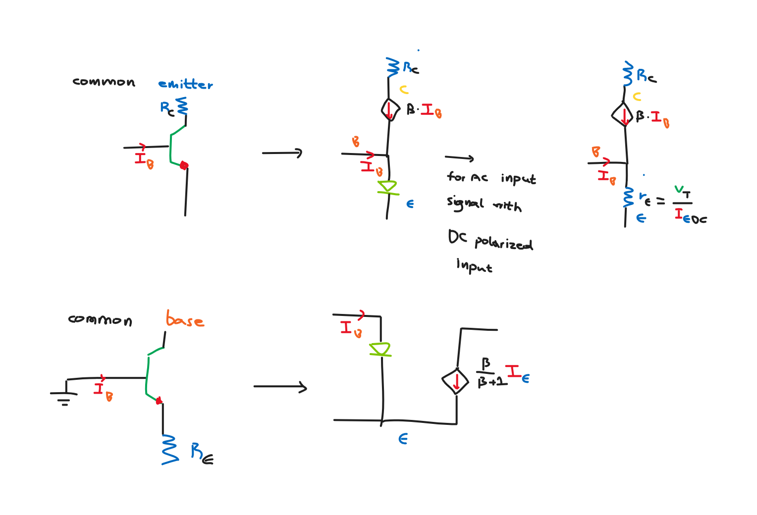
But the Re model for 2 different configurations (common emitter and common base )turns out to be the same!
I don't know why I am really confused.How is this possible?
2 answers
You are accessing this answer with a direct link, so it's being shown above all other answers regardless of its score. You can return to the normal view.
I never would recommend to use the "re model" for a BJT. The reason is as follows:
- The BJT is a voltage-controlled device (Ic is controlled by Vbe and the base current is an unwanted by-product).
- Hence, the characteristic transfer parameter is the transconductance gm=d(Ic)/d(Vbe)=Ic/Vt..
- The obscure quantity re is nothing else than re=1/gm. And it is not correct to say "re is the intrinsic emitter resistance" as we can read in some contributions. This is simply wrong!
- The quantity re can be used (instead of gm) in an equivalent small-signal diagram - however, this can lead to confusion and misunderstandings because such a resistance in the emitter leg can be mixed with a real ohmic external resistor which provides current-controlled voltage feedback.
- I see absolutely no reason to use such a confusing model which does not reflect the real BJT principle based on the transconduchtance gm.
- As an example for the mentioned confusion look at the 5 small diagrams as given in the first post: We can se "re" and "RE" - both with a symbol for the resistor. Are they identical or not?
I'm not sure what you mean by the "Re" model, but ultimately the transistor does a certain thing regardless of what label we put on the circuit it is in.
For a NPN like you're modeling, you will have base current going into the base and coming out the emitter, and collector current going into the collector also coming out of the emitter. If you consider β the gain of the transistor and the magnitude of the base current 1, then the collector current is β, and the emitter current β+1. This is true regardless of the external circuit, so long as the C-E voltage is enough to keep the transistor in its "linear" region, and no maximums are violated.
Different circuit may use a transistor in different ways, but what the transistor does, and therefore its model, remains the same. At most, some circuits may exploit different regions of the transistor's operating range, which might lead to different simplified models.
0 comment threads


0 comment threads