Post History
Around the 19 min mark in the video (approximately, found with hovering the cursor over the timeline) you'll see that different capacitors have different values of both capacitances and parasitics,...
#1: Initial revision
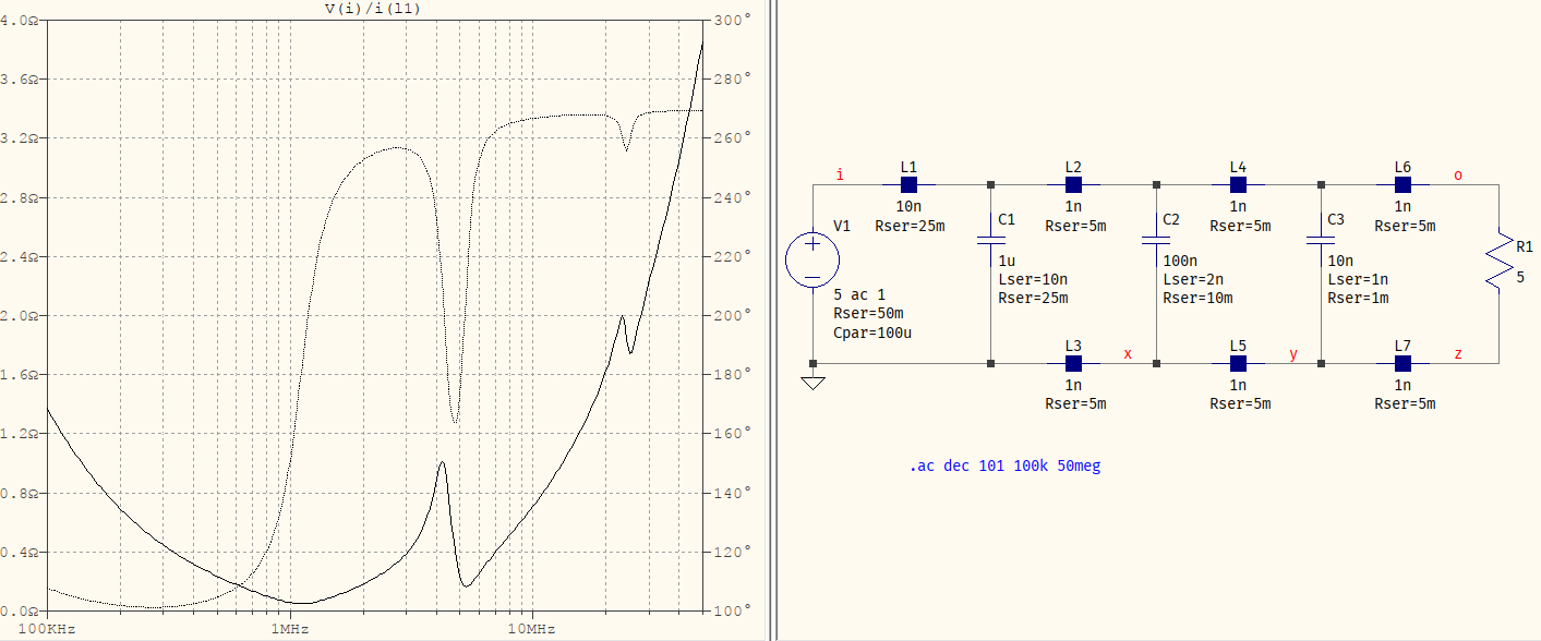
Around the 19 min mark in the video (approximately, found with hovering the cursor over the timeline) you'll see that different capacitors have different values of both capacitances and parasitics, and their combined response causes those peaks. Not lastly, there are PCB traces that come with both their characteristic impedance, and parasitics. It may be more intuitive to use a SPICE program to simulate a possible setup. Everything may look something like this:  I've used some fairly sensible values: a slightly larger, but short trace from the "supply (`V1`) to the PCB, tightly placed capacitors with some common values for the parasitics. If you want a mathematical analysis then feel free to go for it, but I'll warn you you'd be getting with a very fluffy expression, which is likely to obscure things, rather than not. That's why the picture above should be slightly better, and the video even more.


