Post History
#20: Post edited
by
 Circuit fantasist
·
2022-09-14T17:33:01Z (almost 3 years ago)
Circuit fantasist
·
2022-09-14T17:33:01Z (almost 3 years ago)
Added link
- It was a big challenge for me to show the basic idea behind the [op-amp instrumentation amplifier](https://electrical.codidact.com/posts/285392) by building and reinventing it step by step. But it is no less challenging to show the idea behind the simpler but legendary _transistor differential amplifier_ (figuratively named "long-tailed pair"). I will do it here in the same inventive way by sequentially building basic transistor amplifier stages known as _common emitter_, _common base_ and _common collector_ transistor amplifier stage. I will show it conceptually on the blackboard and practically on the prototyping board. In addition, I will suggest a classification with more meaningful names - _base-driven_, _emitter-driven_, _base-driven with negative feedback_ and _base-emitter driven_ transistor amplifier stage.
- # Building the circuit
- ## What is an amplifier?
- In the literal sense of the word, there is no (energy) amplification. It is not possible to get a large power from a small one because this would violate the law of energy conservation (energy can only be converted). "Amplification" actually means "regulation". Here is a simple intuitive explanation of this trick…
- ## Amplifier with a current output...
- To make an "amplifier", we connect a regulating element (transistor T) in series with the supply voltage source Vcc and begin to control its "resistance" through the input voltage Vin. As a result, the current Ic starts to change.
- 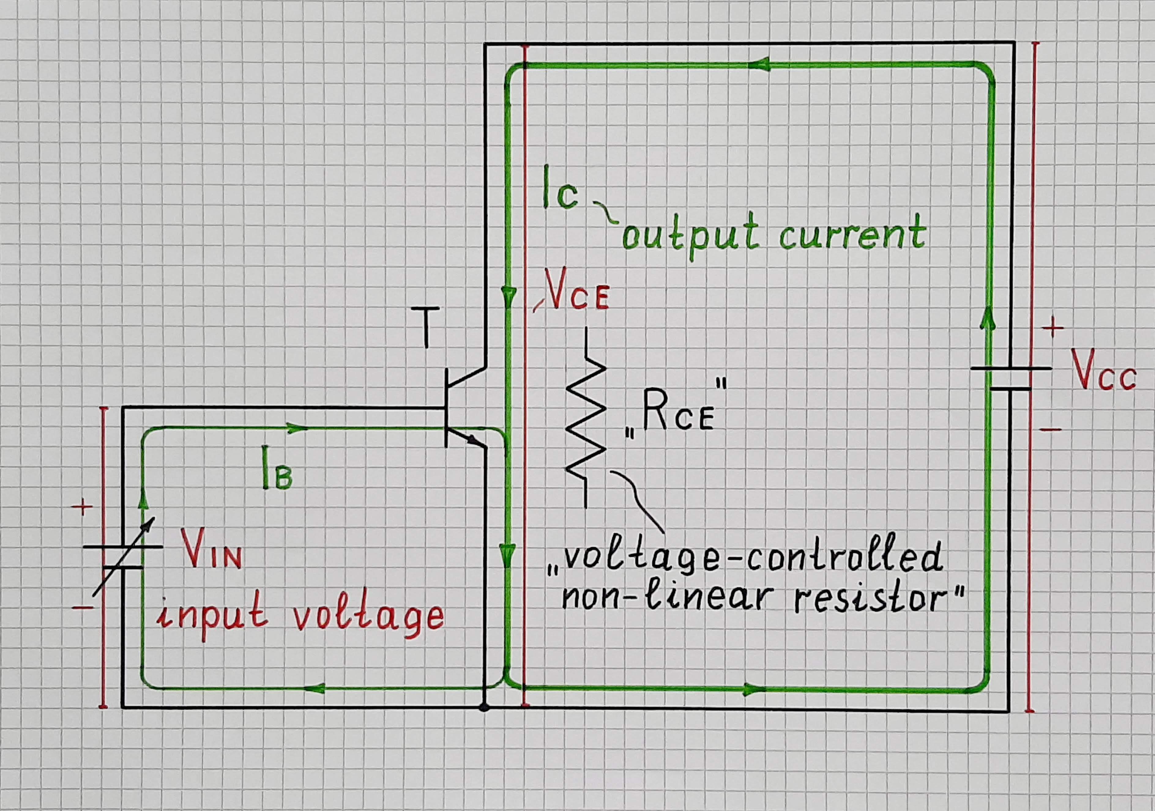
- I think this is the simplest possible "functional" explanation of how a transistor works. If you do not like the word "resistance", add "nonlinear" before it. If you still do not agree, then I would ask you, "What other common property besides resistance does a transistor have to be able to regulate the current in a circuit?"
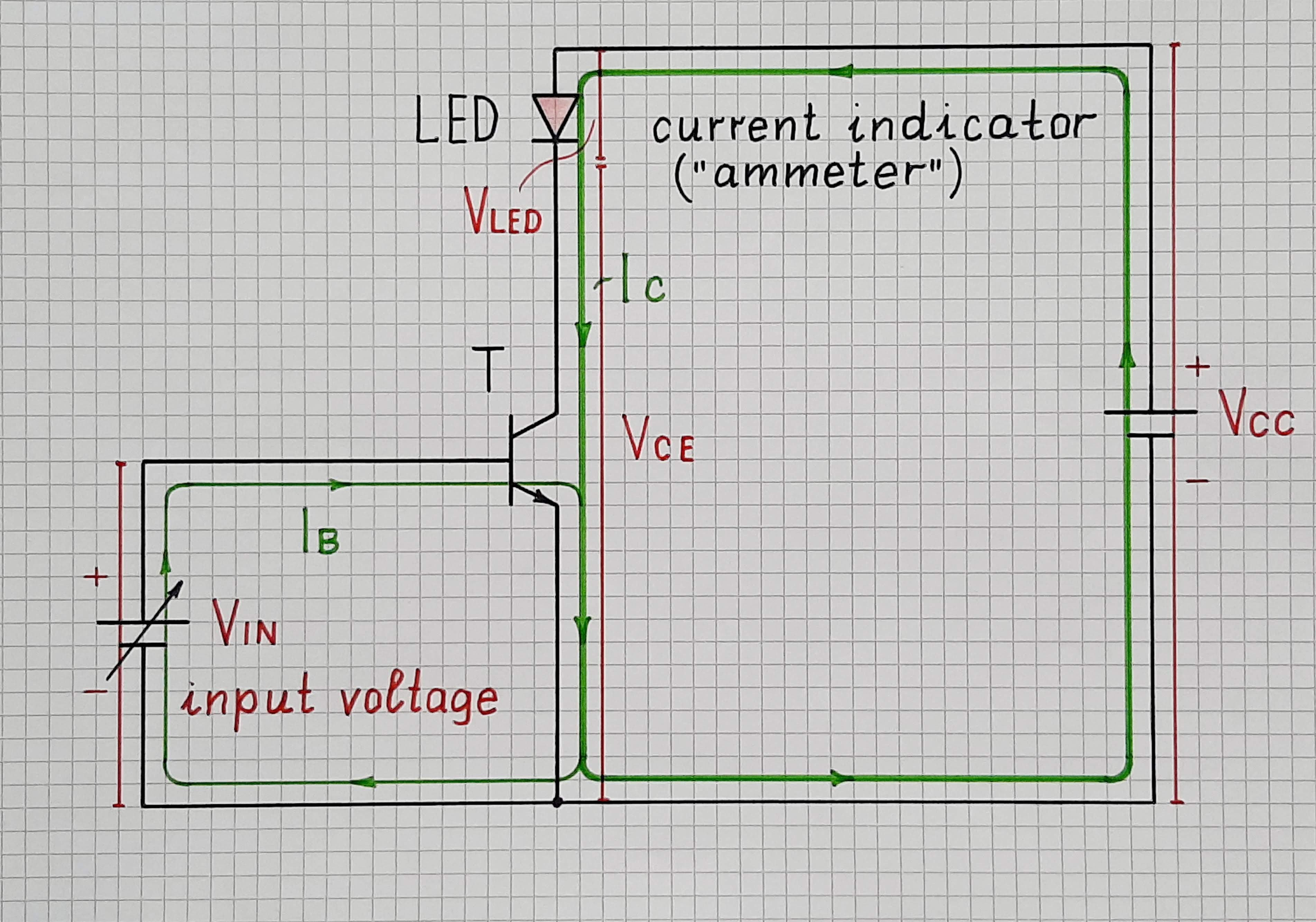
- ## ... indicated by an LED
- In addition to the classic ammeter, we can monitor the current with the help of an LED (the intensity of its light gives us an idea of the current magnitude).
- 
- ## Amplifier with a voltage output…
- But we need a voltage amplifier. For this purpose, we need to convert the output current Ic into an output voltage Vout. To do this, we include a resistor Rc in the output circuit and a "non-inverted" drop VRc = Ic.Rc appears across it ("non-inverted" in the sense that when the input voltage increases, the output also increases in absolute value).
- 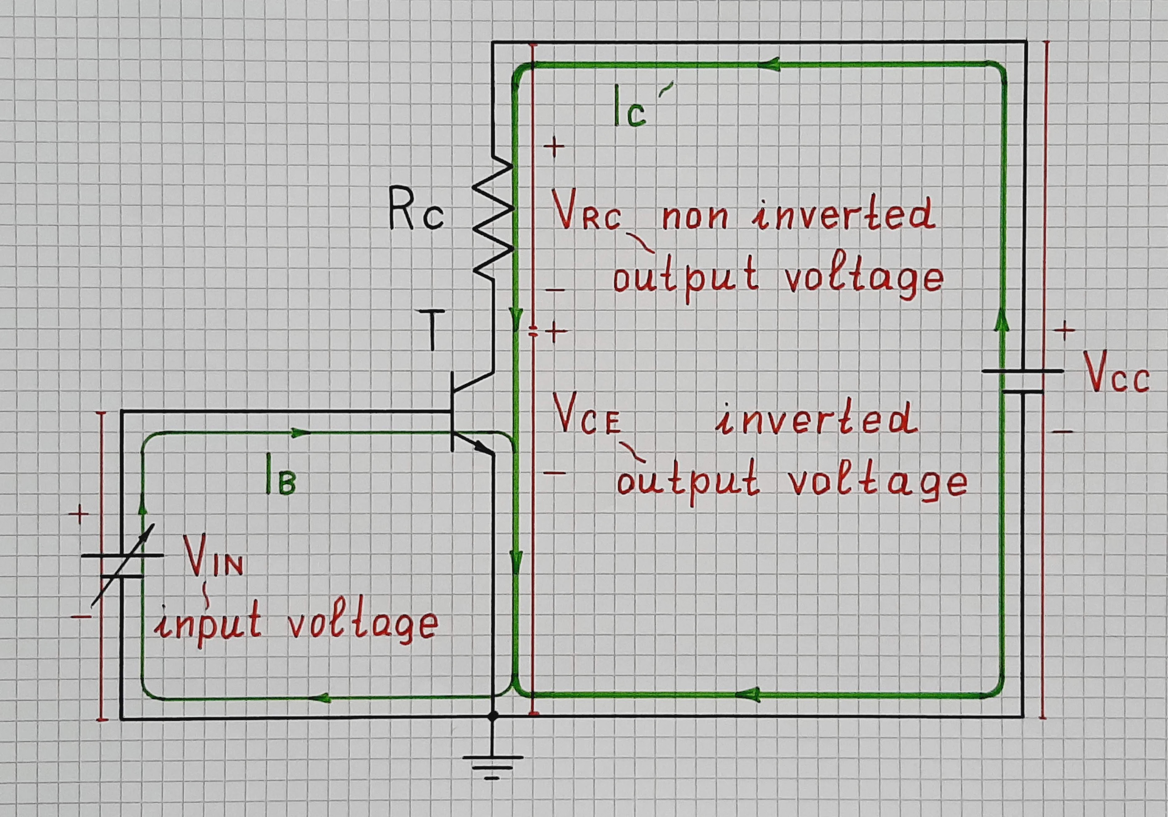
- We can also use the complement of this drop to the supply voltage as an "inverted" output voltage Vce ("inverted" in the sense that when the input voltage increases, the output also increases in absolute value). This gives us the simplest transistor amplifier configuration, known as common emitter, in which the input voltage is applied to the base and the emitter is connected to ground.
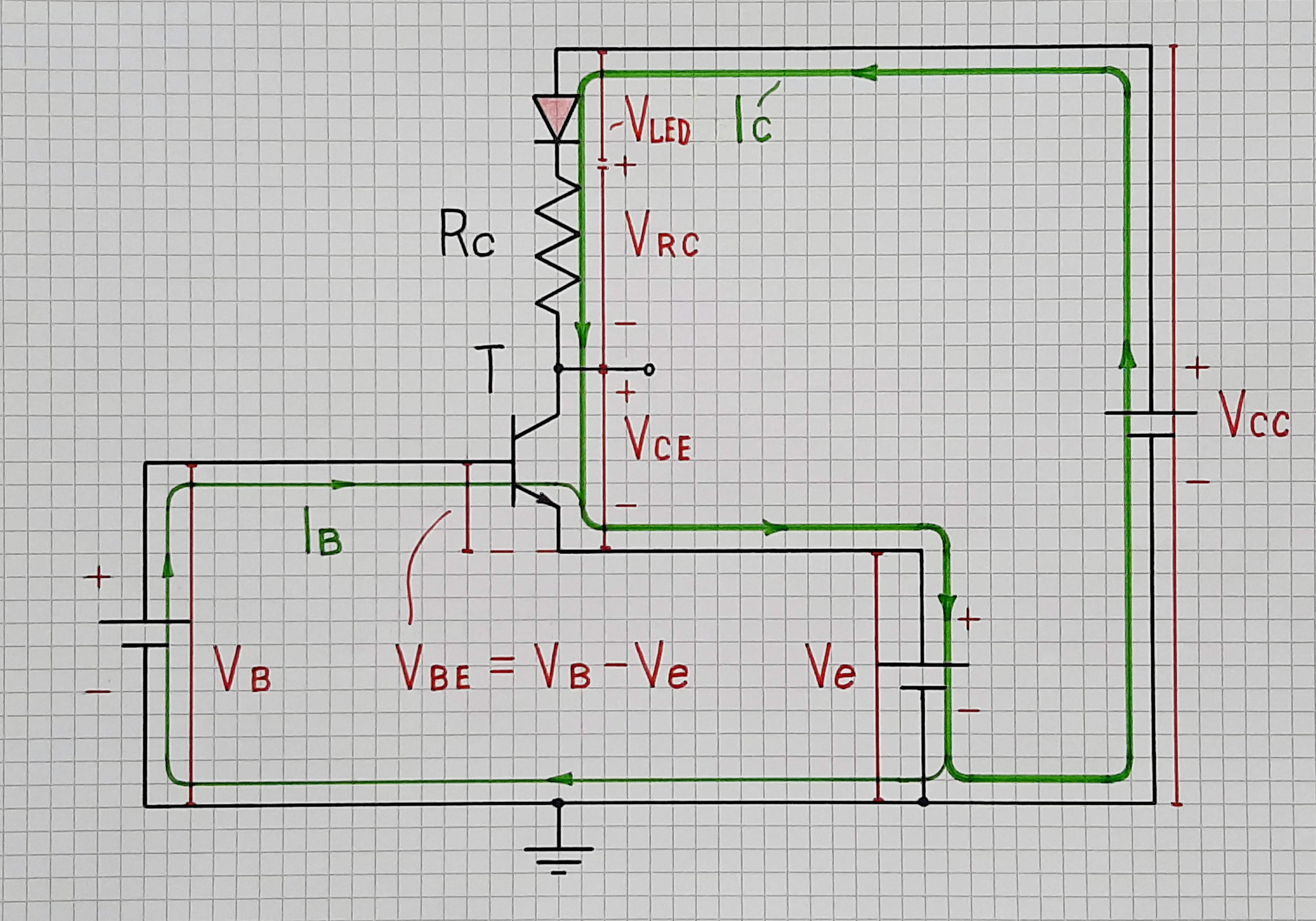
- ## The transistor input voltage as a difference of two input voltages
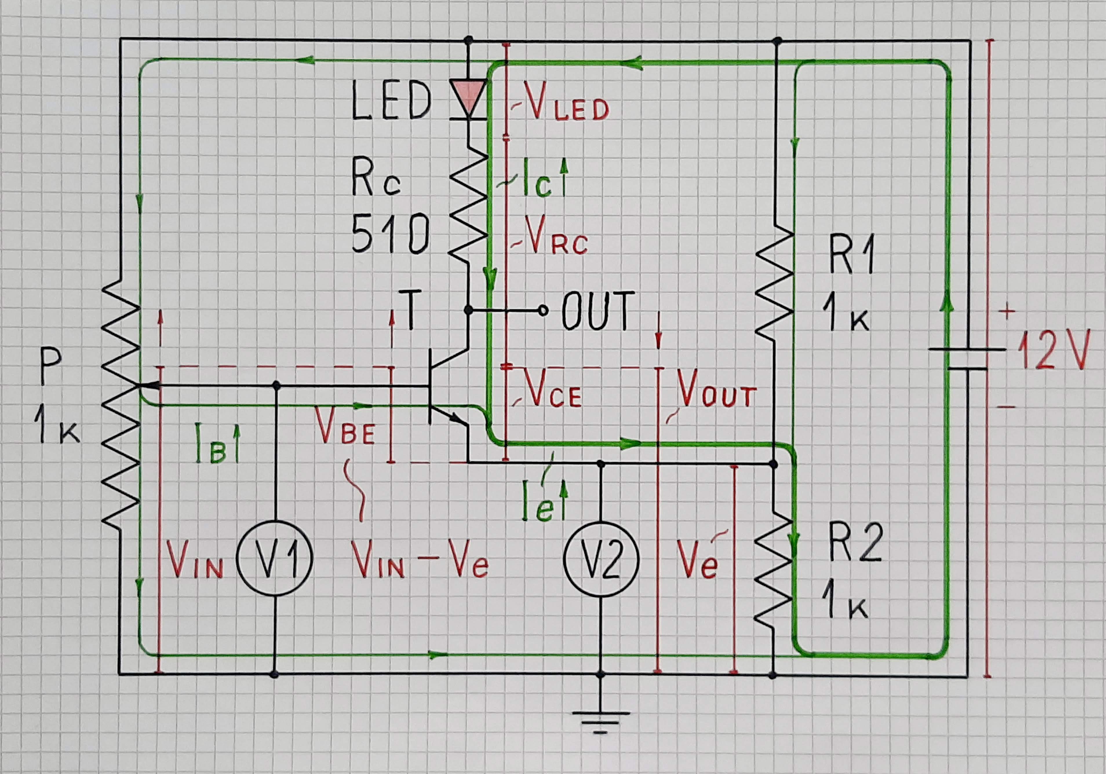
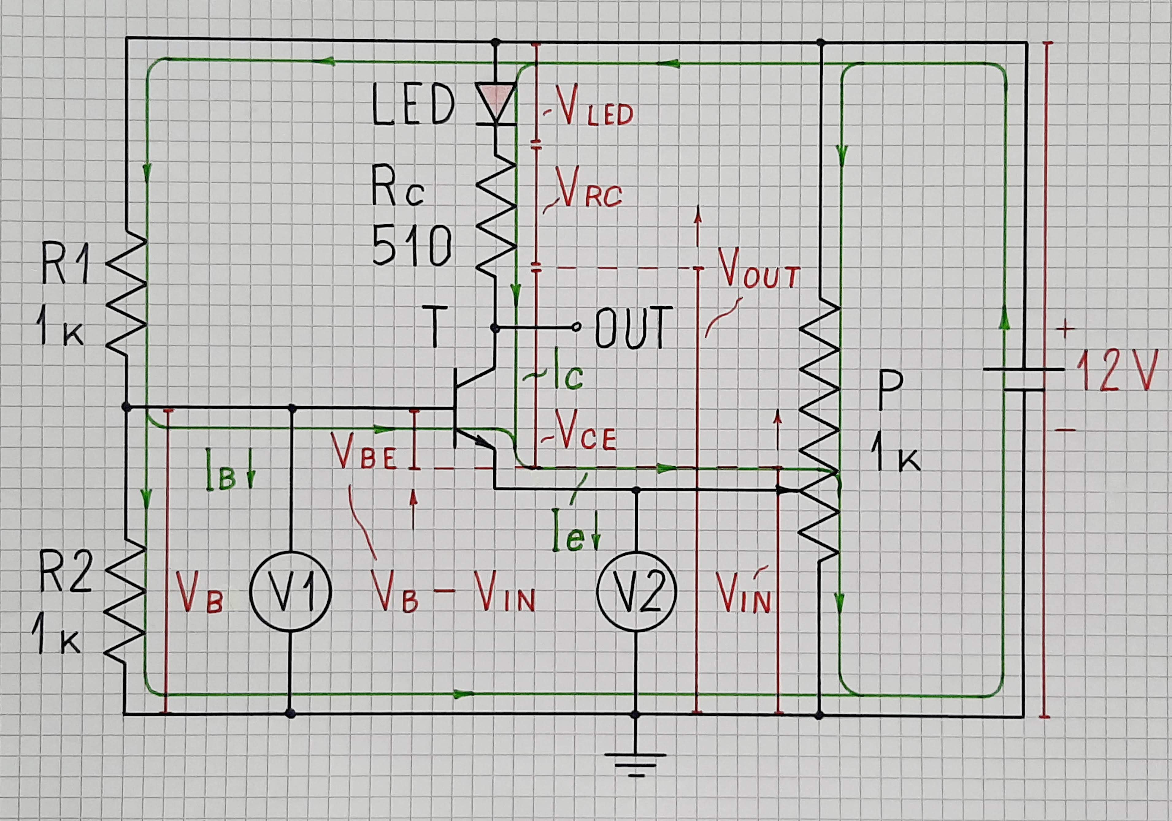
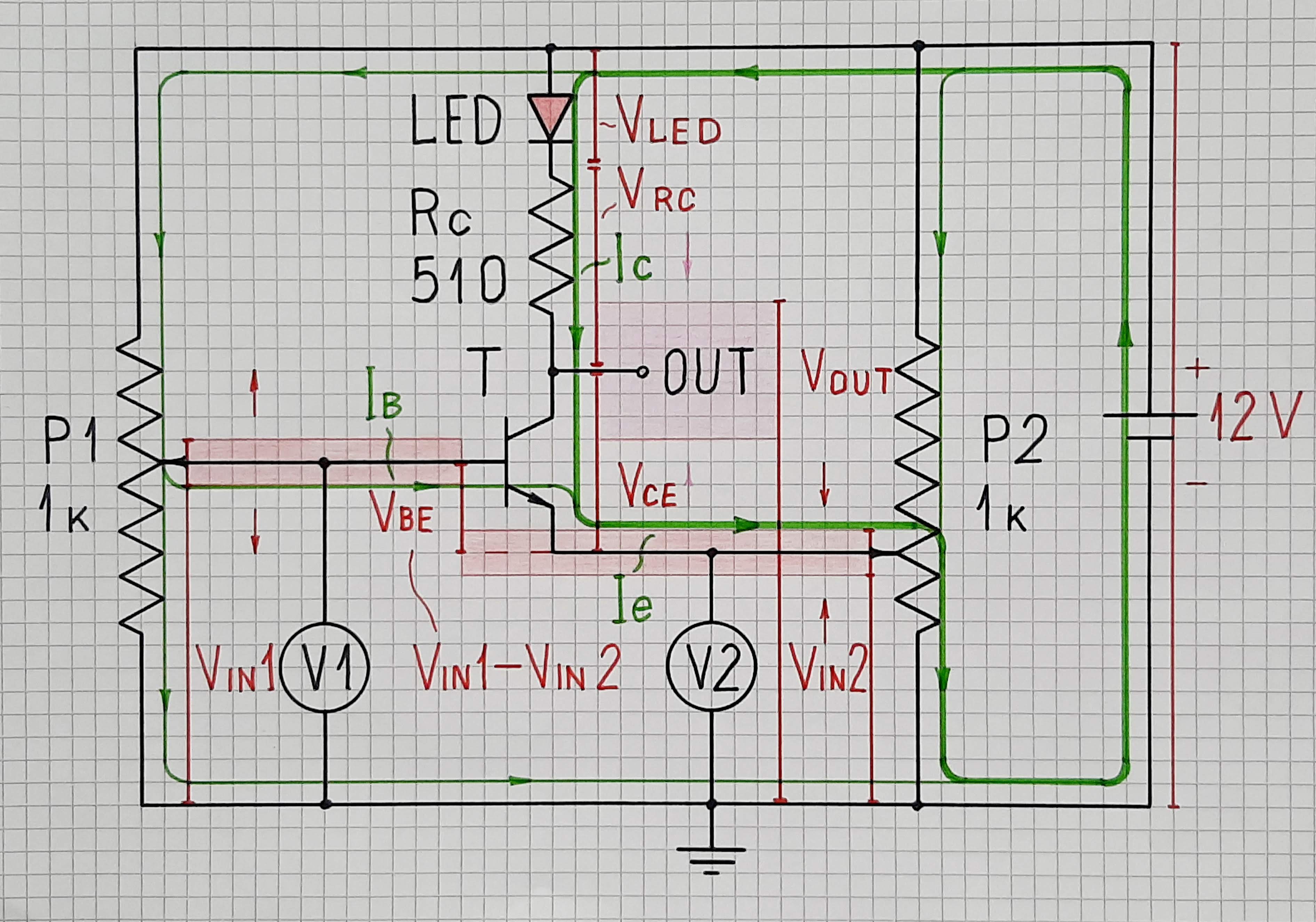
- If we apply a second voltage Ve to the emitter, the possibilities to control the transistor increase and we can get more versions of transistor amplifier stages - _common base_, _common collector_, _differential amplifier_. Now the "true" input voltage Vbe of the transistor is the difference of the two voltages Vb and Ve. Vbe is a differential, "floating" (ungrounded) voltage, and Vb and Ve are single-ended voltages measured with respect to ground.
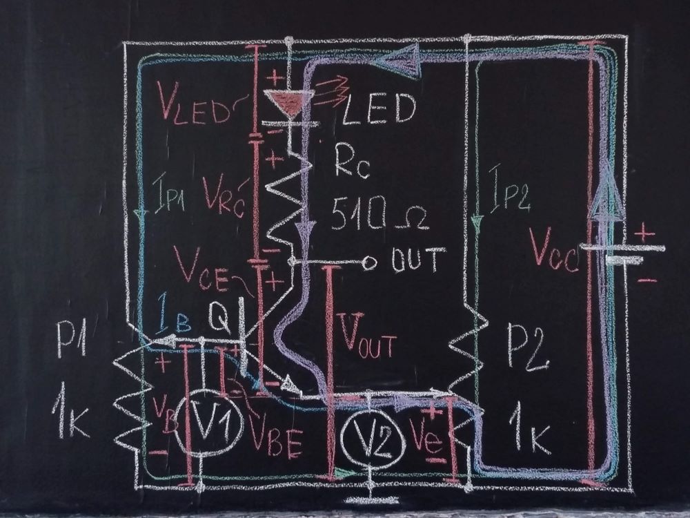
- 
- The voltages are represented on the circuit diagram by voltage bars with proportional height (in red)... and the currents - by current loops with related thickness (in green). See also my papers [What are voltages in circuits?](https://electrical.codidact.com/posts/284860) and [Where do currents flow in circuits?](https://electrical.codidact.com/posts/284816)
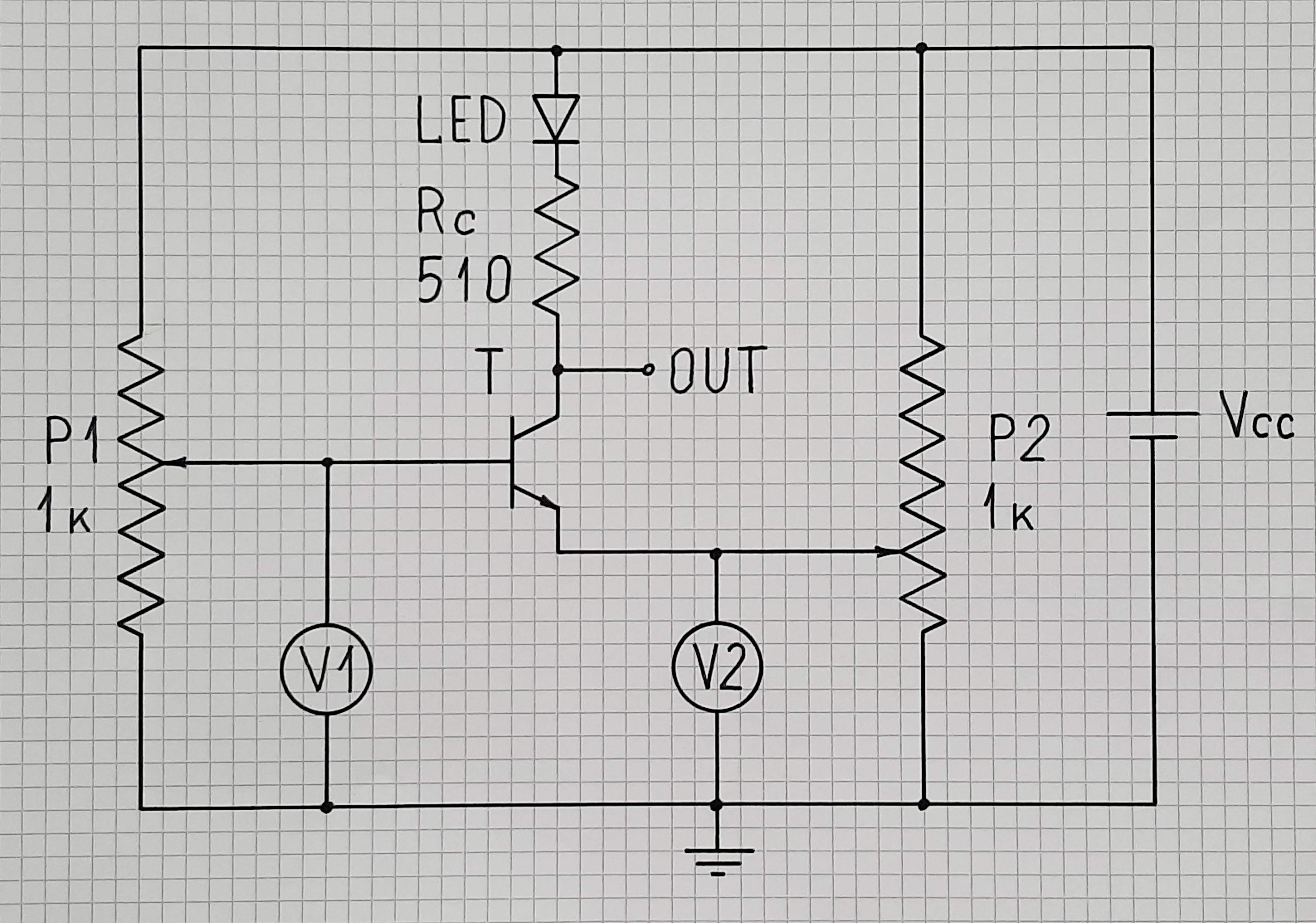
- ## Practical circuit
- ### ... diagram
- The two voltages Vb and Ve are "produced" by 1 k linear potentiometers (P1 and P2) and applied to the base and emitter of the transistor (BC547C)... and a LED (VQA13) is connected in series to the collector resistor Rc. The voltages were measured by the voltmeters V1 and V2 and the collector current (transistor state) is indicated by the LED. When one of the voltages is constant, we will draw a discrete voltage divider instead of a potentiometer, but in practice we will get it through a potentiometer, on which we keep the wiper stationary.
- 
- ### ... on the blackboard
- 
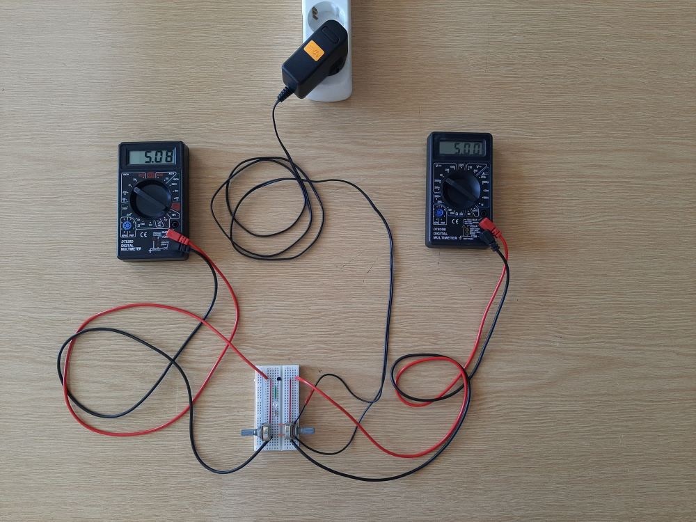
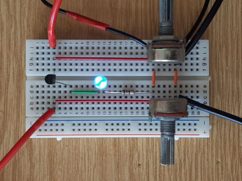
- # Implementing the circuit on the prototyping board
- 
- 
- # Exploring various basic transistor circuits
- ## Base-driven (common-emitter) transistor stage
- In this case, we apply some constant voltage Ve to the emitter and initially, approximately the same base voltage Vb. We then begin to vary carefully, within small limits, the base voltage as the input voltage Vin.
- 
- We see that when the base voltage exceeds the emitter voltage by about 600 mV, the transistor begins conducting. The collector current increases and the LED starts to glow (see the [movie](https://photos.app.goo.gl/Fuvr56p5euGnU7Cz5)). The voltage drop across the collector resistor begins to grow, and its complement to Vcc, the voltage Vce, decreases. Therefore, the circuit is _inverting_.
- **Analogy.** An op-amp with grounded (or with fixed voltage) non-inverting input resembles the common-emitter transistor stage:
- * op-amp inverting input = transistor base
- * op-amp non-inverting input = transistor emitter
- * op-amp output = transistor collector
- ## Emitter-driven (common-base) transistor stage
- Now we swap the roles by applying a constant voltage Vb to the base and initially, approximately the same emitter voltage Ve. We then begin to vary carefully, within small limits, the emitter voltage as the input Vin.
- 
- For example, if the emitter voltage approaches the base voltage by less than 600 mV, the transistor starts to turn off. The collector current decreases and the LED starts to glow (see the [movie](https://photos.app.goo.gl/GdkfeDkUmfRf47DL9)). The voltage drop across the collector resistor begins to decrease and its complement to Vcc, the voltage Vce, to increase. Therefore, the circuit is _non-inverting_.
- But here we notice an unpleasant moment - the large collector current flows through the input source. This means that the circuit has a small input resistance.
- **Analogy.** An op-amp with grounded (or with fixed voltage) inverting input resembles the common-base transistor stage:
- * op-amp non-inverting input = transistor emitter
- * op-amp inverting input = transistor base
- * op-amp output = transistor collector
- See also [another movie](https://photos.app.goo.gl/XmyMFrxVmi8jByDf7) in the laboratory on Basic Electronics (April 16, 2019).
- ## Base-driven with feedback (common-collector) transistor stage
- In this case, as the base voltage increases, the transistor begins to conduct more and more and let more and more collector current pass through the emitter resistor (the LED starts to glow more and more brightly). Figuratively speaking, the transistor "lifts" its emitter thus decreasing the input voltage. The name of this trick is "emitter degeneration", "bootstrapping" or "voltage following negative feedback".
- 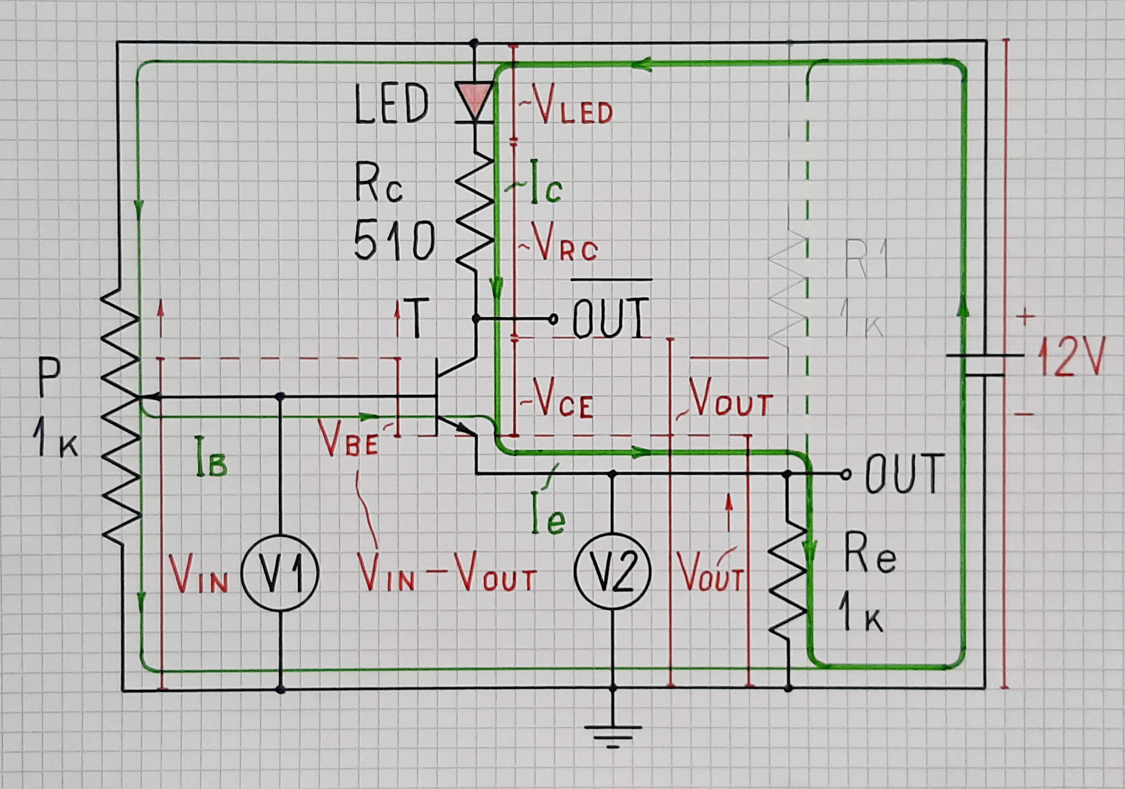
- The voltage drop across the collector resistor grows, but this does not really matter in this case. More significantly, the emitter voltage rises and tends to equal the base voltage ("follows" it, hence the name "emitter follower").
- **Analogy.** An op-amp follower resembles the common-collector transistor stage:
- * op-amp non-inverting input = transistor base
- * op-amp inverting input = transistor emitter
- * op-amp output = transistor emitter
- ## Base-emitter driven transistor ("differential amplifier")
- We can extend our experiments if we start varying both voltages at the same time. Thus, we imperceptibly "invent" the prototype of the _differential amplifier_.
- **Analogy.** An op-amp without grounded inputs resembles the transistor differential stage:
- * op-amp inverting input = transistor base
- * op-amp non-inverting input = transistor emitter
- * op-amp output = transistor collector
- We have two options to change the input voltages:
- ### … in the same direction (common mode)
- First, let's vary both voltages Vb and Ve (move both potentiometer wipers) simultaneously and in the same direction. As a result, the input voltage Vbe, the collector current Ic and the output voltage Vout do not change, i.e. the circuit does not amplify. It is interesting that, in this simple 1-transistor "differential amplifier", they don't change at all... while, in the true 2-transistor differential amplifier, they do change to some extent!
- 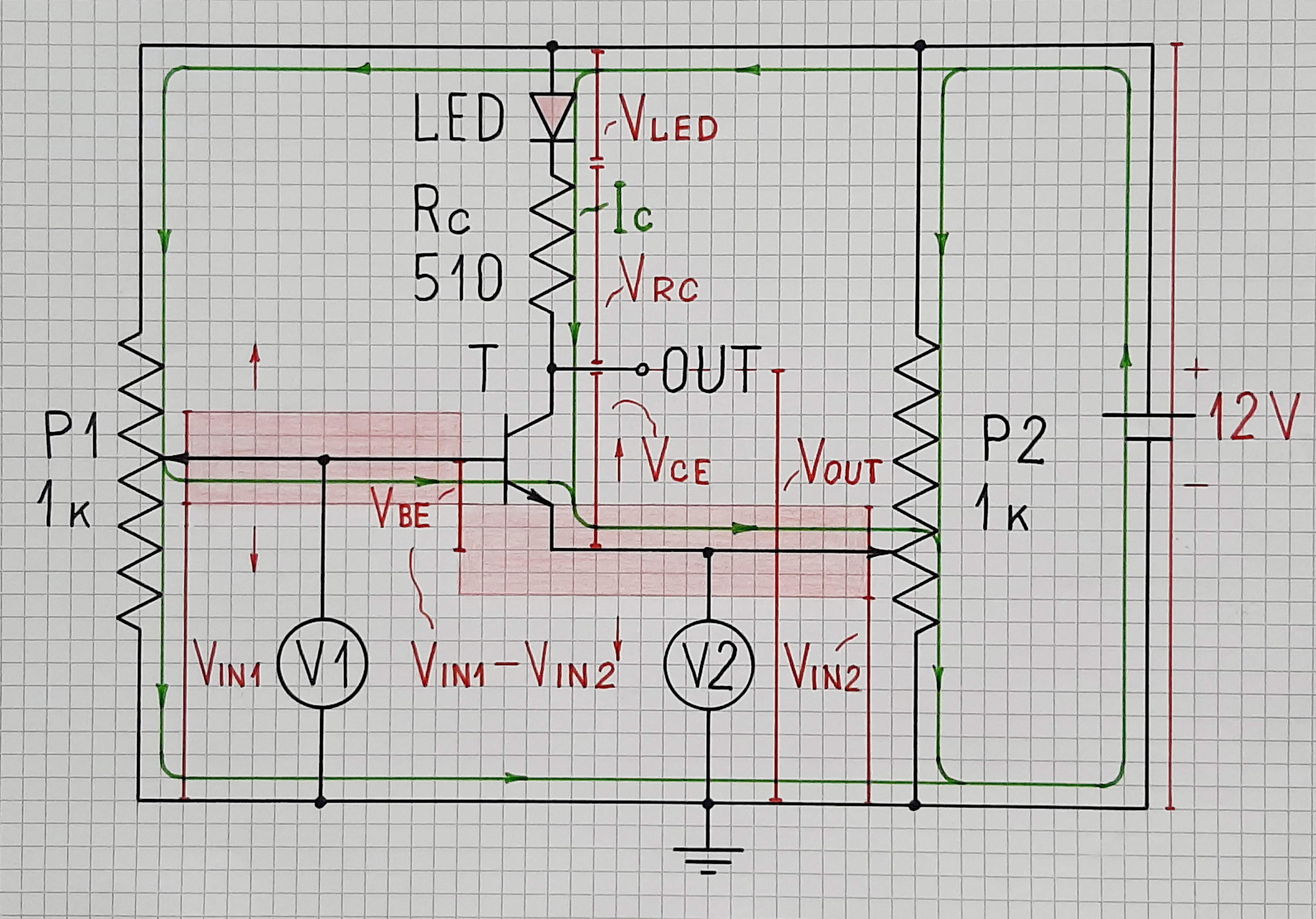
- ### … in the opposite directions (differential mode)
- Let's now start varying both voltages Vb and Ve (move both wipers) simultaneously but in different directions (opposite). Now the input voltage Vbe, the collector current Ic and the output voltage Vout drastically change, ie. the circuit amplifies a lot.
- 
- ## True differential amplifier
- This was the prelude to the true 2-transistor differential amplifier (_long-tailed pair_). Let's now see how we can transform the imperfect 1-transistor "differential amplifier" into true differential amplifier...
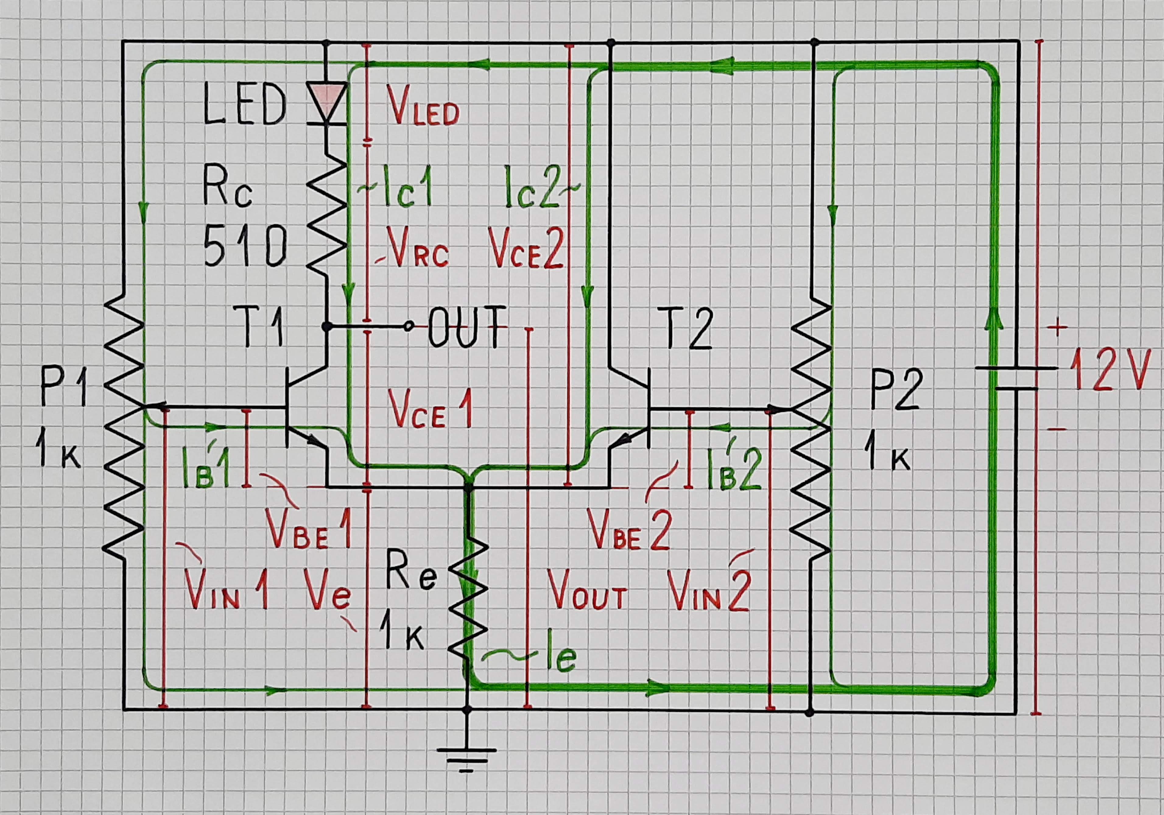
- ### Making circuit symmetrical
- **Problem.** Obviously, the disadvantage of the 1-transistor "differential amplifier" is its asymmetry - _beta +1_ times more current flows through the voltage source connected to the emitter compared to the source connected to the base.
- **Remedy.** To make the circuit symmetrical, we can include another emitter follower between the voltage source and the emitter.
- 
- Problem solved... but another problem appears. Let's see what it is..
- ### Removing the common-mode error
- **Background.** Our differential amplifier has a differential input but its output is not differential; it is referenced to ground, asymmetrical or, as they say, "single-ended". This is because, in most cases, we want it to be. But we want the voltage at this output to not change when both input voltages change at the same time, in the same direction and to the same extent (the so-called "common mode").
- In this mode, the two emitter followers help each other to drive a common load - the emitter resistor Re. The role of this resistor is to pass the emitter currents to ground. Figuratively speaking, this resistor "pulls down" the common emitter point while the transistors "pull" it up.
- **Problem** is because they do that by current. When the input voltages change, the transistors change their collector currents so that to change the voltage drop across the emitter resistor in the same manner. As a result, the voltage drop VRc across the collector resistor Rc changes as well... and it should not...
- **Remedy.** Maybe you expect me to suggest straight away that we replace the emitter resistor with a current source as the textbooks say? I am going to disappoint you a bit because I think it is better to naturally reach this idea ourselves... and even experiment with it on our setup.
- The trick is extremely simple but clever. We want the current through the emitter resistor not to change when the voltage drop across the resistor, for example, increases... ie, the ratio VRc/Rc = Ie not to change when the numerator VRc increases. So the solution is ***to increase the denominator Rc to the same extent***.
- **Modeling.** We can model the trick on our setup by replacing the constant emitter resistor with a variable one. For this purpose, we can take another (third) potentiometer 1 k connected as a rheostat and start rotating it together with the other two. The result will be that Ie, Ic1 and ultimately Vout will not change... which is what we wanted to do.
- 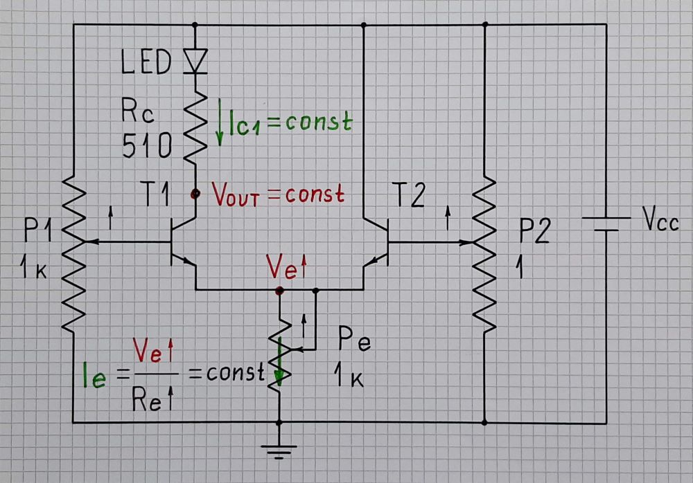
- **Implementation.** Behaving in this way, the variable resistor acts as a *dynamic resistor* that maintains a constant current through itself (*current stabilizing element*). This is one way of [making current sources](https://electrical.codidact.com/posts/279592), which is why they denote it by the current source symbol.
- 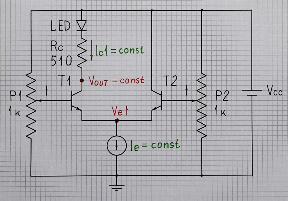
- In practice, it is most often implemented through a [transistor with a constant base voltage](https://electrical.codidact.com/posts/285024).
- 
- # Imperfections
- Our experimental setup is extremely simple, but it still has some drawbacks. Let's see what they are and how we can overcome them.
- 1. Potentiometers have quite high resistance and influence each other through the base-emitter junction, which seems to connect them like a piece of wire. We can reduce this negative effect by replacing them with lower resistance ones but they should be able to dissipate most of the heat.
- 2. There is a danger of damage to the potentiometers or the base-emitter junction if the wipers are given in their extreme opposite positions (the source is given "short"). The solution is to insert a protecting resistor in the circuit.
- # Comparison
- So, what is the difference between the two classifications?
- As we have seen, there is always only one "true" input voltage Vbe applied between the base and emitter (across the base-emitter junction). In most applications, it is floating... but, as a rule, in circuits, input voltages should be grounded (single ended). That is why, for greater versatility and flexibility, we form Vbe as a difference between two input voltages (Vbe = Vb - Ve)... and then vary the one, other or both. We have two ways to name these configurations:
- In the classic centuries old classification, we give the name of the configuration (_common-emitter_, _common-base_, etc.) according to which of the transistor terminals is with a fixed voltage (i.e., what terminal is AC grounded, passive, neutral). But it is the less important terminal, especially in the case of the so-called _common collector_. The bare fact that the collector is AC grounded does not mean anything because the input voltage is not applied between the base and collector. And what about the differential stage where there is no such AC grounded terminal?
- In our classification here, we give the configuration name (base-driven, emitter-driven, etc.) according to which of the transistor terminals is driven by the input voltage (i.e., what terminal is active) that is more meaningful.
- # Web resources
- [Common Base Amplifier Confusion](https://electronics.stackexchange.com/a/540841/61398) is my answer in StackExchange related to this paper
[How do we investigate basic transistor amplifier stages?](https://circuitstories.blogspot.com/2022/08/how-do-we-investigate-basic-transistor.html) is the same but enlarged story in my blog [Circuit Stories](https://circuitstories.blogspot.com/)
- It was a big challenge for me to show the basic idea behind the [op-amp instrumentation amplifier](https://electrical.codidact.com/posts/285392) by building and reinventing it step by step. But it is no less challenging to show the idea behind the simpler but legendary _transistor differential amplifier_ (figuratively named "long-tailed pair"). I will do it here in the same inventive way by sequentially building basic transistor amplifier stages known as _common emitter_, _common base_ and _common collector_ transistor amplifier stage. I will show it conceptually on the blackboard and practically on the prototyping board. In addition, I will suggest a classification with more meaningful names - _base-driven_, _emitter-driven_, _base-driven with negative feedback_ and _base-emitter driven_ transistor amplifier stage.
- # Building the circuit
- ## What is an amplifier?
- In the literal sense of the word, there is no (energy) amplification. It is not possible to get a large power from a small one because this would violate the law of energy conservation (energy can only be converted). "Amplification" actually means "regulation". Here is a simple intuitive explanation of this trick…
- ## Amplifier with a current output...
- To make an "amplifier", we connect a regulating element (transistor T) in series with the supply voltage source Vcc and begin to control its "resistance" through the input voltage Vin. As a result, the current Ic starts to change.
- 
- I think this is the simplest possible "functional" explanation of how a transistor works. If you do not like the word "resistance", add "nonlinear" before it. If you still do not agree, then I would ask you, "What other common property besides resistance does a transistor have to be able to regulate the current in a circuit?"
- ## ... indicated by an LED
- In addition to the classic ammeter, we can monitor the current with the help of an LED (the intensity of its light gives us an idea of the current magnitude).
- 
- ## Amplifier with a voltage output…
- But we need a voltage amplifier. For this purpose, we need to convert the output current Ic into an output voltage Vout. To do this, we include a resistor Rc in the output circuit and a "non-inverted" drop VRc = Ic.Rc appears across it ("non-inverted" in the sense that when the input voltage increases, the output also increases in absolute value).
- 
- We can also use the complement of this drop to the supply voltage as an "inverted" output voltage Vce ("inverted" in the sense that when the input voltage increases, the output also increases in absolute value). This gives us the simplest transistor amplifier configuration, known as common emitter, in which the input voltage is applied to the base and the emitter is connected to ground.
- ## The transistor input voltage as a difference of two input voltages
- If we apply a second voltage Ve to the emitter, the possibilities to control the transistor increase and we can get more versions of transistor amplifier stages - _common base_, _common collector_, _differential amplifier_. Now the "true" input voltage Vbe of the transistor is the difference of the two voltages Vb and Ve. Vbe is a differential, "floating" (ungrounded) voltage, and Vb and Ve are single-ended voltages measured with respect to ground.
- 
- The voltages are represented on the circuit diagram by voltage bars with proportional height (in red)... and the currents - by current loops with related thickness (in green). See also my papers [What are voltages in circuits?](https://electrical.codidact.com/posts/284860) and [Where do currents flow in circuits?](https://electrical.codidact.com/posts/284816)
- ## Practical circuit
- ### ... diagram
- The two voltages Vb and Ve are "produced" by 1 k linear potentiometers (P1 and P2) and applied to the base and emitter of the transistor (BC547C)... and a LED (VQA13) is connected in series to the collector resistor Rc. The voltages were measured by the voltmeters V1 and V2 and the collector current (transistor state) is indicated by the LED. When one of the voltages is constant, we will draw a discrete voltage divider instead of a potentiometer, but in practice we will get it through a potentiometer, on which we keep the wiper stationary.
- 
- ### ... on the blackboard
- 
- # Implementing the circuit on the prototyping board
- 
- 
- # Exploring various basic transistor circuits
- ## Base-driven (common-emitter) transistor stage
- In this case, we apply some constant voltage Ve to the emitter and initially, approximately the same base voltage Vb. We then begin to vary carefully, within small limits, the base voltage as the input voltage Vin.
- 
- We see that when the base voltage exceeds the emitter voltage by about 600 mV, the transistor begins conducting. The collector current increases and the LED starts to glow (see the [movie](https://photos.app.goo.gl/Fuvr56p5euGnU7Cz5)). The voltage drop across the collector resistor begins to grow, and its complement to Vcc, the voltage Vce, decreases. Therefore, the circuit is _inverting_.
- **Analogy.** An op-amp with grounded (or with fixed voltage) non-inverting input resembles the common-emitter transistor stage:
- * op-amp inverting input = transistor base
- * op-amp non-inverting input = transistor emitter
- * op-amp output = transistor collector
- ## Emitter-driven (common-base) transistor stage
- Now we swap the roles by applying a constant voltage Vb to the base and initially, approximately the same emitter voltage Ve. We then begin to vary carefully, within small limits, the emitter voltage as the input Vin.
- 
- For example, if the emitter voltage approaches the base voltage by less than 600 mV, the transistor starts to turn off. The collector current decreases and the LED starts to glow (see the [movie](https://photos.app.goo.gl/GdkfeDkUmfRf47DL9)). The voltage drop across the collector resistor begins to decrease and its complement to Vcc, the voltage Vce, to increase. Therefore, the circuit is _non-inverting_.
- But here we notice an unpleasant moment - the large collector current flows through the input source. This means that the circuit has a small input resistance.
- **Analogy.** An op-amp with grounded (or with fixed voltage) inverting input resembles the common-base transistor stage:
- * op-amp non-inverting input = transistor emitter
- * op-amp inverting input = transistor base
- * op-amp output = transistor collector
- See also [another movie](https://photos.app.goo.gl/XmyMFrxVmi8jByDf7) in the laboratory on Basic Electronics (April 16, 2019).
- ## Base-driven with feedback (common-collector) transistor stage
- In this case, as the base voltage increases, the transistor begins to conduct more and more and let more and more collector current pass through the emitter resistor (the LED starts to glow more and more brightly). Figuratively speaking, the transistor "lifts" its emitter thus decreasing the input voltage. The name of this trick is "emitter degeneration", "bootstrapping" or "voltage following negative feedback".
- 
- The voltage drop across the collector resistor grows, but this does not really matter in this case. More significantly, the emitter voltage rises and tends to equal the base voltage ("follows" it, hence the name "emitter follower").
- **Analogy.** An op-amp follower resembles the common-collector transistor stage:
- * op-amp non-inverting input = transistor base
- * op-amp inverting input = transistor emitter
- * op-amp output = transistor emitter
- ## Base-emitter driven transistor ("differential amplifier")
- We can extend our experiments if we start varying both voltages at the same time. Thus, we imperceptibly "invent" the prototype of the _differential amplifier_.
- **Analogy.** An op-amp without grounded inputs resembles the transistor differential stage:
- * op-amp inverting input = transistor base
- * op-amp non-inverting input = transistor emitter
- * op-amp output = transistor collector
- We have two options to change the input voltages:
- ### … in the same direction (common mode)
- First, let's vary both voltages Vb and Ve (move both potentiometer wipers) simultaneously and in the same direction. As a result, the input voltage Vbe, the collector current Ic and the output voltage Vout do not change, i.e. the circuit does not amplify. It is interesting that, in this simple 1-transistor "differential amplifier", they don't change at all... while, in the true 2-transistor differential amplifier, they do change to some extent!
- 
- ### … in the opposite directions (differential mode)
- Let's now start varying both voltages Vb and Ve (move both wipers) simultaneously but in different directions (opposite). Now the input voltage Vbe, the collector current Ic and the output voltage Vout drastically change, ie. the circuit amplifies a lot.
- 
- ## True differential amplifier
- This was the prelude to the true 2-transistor differential amplifier (_long-tailed pair_). Let's now see how we can transform the imperfect 1-transistor "differential amplifier" into true differential amplifier...
- ### Making circuit symmetrical
- **Problem.** Obviously, the disadvantage of the 1-transistor "differential amplifier" is its asymmetry - _beta +1_ times more current flows through the voltage source connected to the emitter compared to the source connected to the base.
- **Remedy.** To make the circuit symmetrical, we can include another emitter follower between the voltage source and the emitter.
- 
- Problem solved... but another problem appears. Let's see what it is..
- ### Removing the common-mode error
- **Background.** Our differential amplifier has a differential input but its output is not differential; it is referenced to ground, asymmetrical or, as they say, "single-ended". This is because, in most cases, we want it to be. But we want the voltage at this output to not change when both input voltages change at the same time, in the same direction and to the same extent (the so-called "common mode").
- In this mode, the two emitter followers help each other to drive a common load - the emitter resistor Re. The role of this resistor is to pass the emitter currents to ground. Figuratively speaking, this resistor "pulls down" the common emitter point while the transistors "pull" it up.
- **Problem** is because they do that by current. When the input voltages change, the transistors change their collector currents so that to change the voltage drop across the emitter resistor in the same manner. As a result, the voltage drop VRc across the collector resistor Rc changes as well... and it should not...
- **Remedy.** Maybe you expect me to suggest straight away that we replace the emitter resistor with a current source as the textbooks say? I am going to disappoint you a bit because I think it is better to naturally reach this idea ourselves... and even experiment with it on our setup.
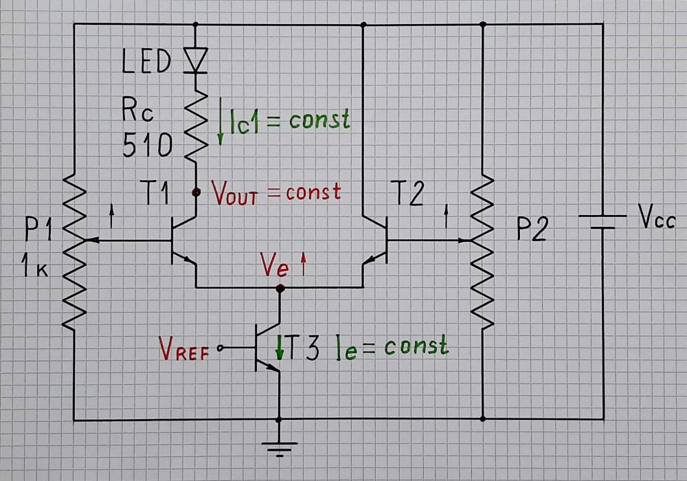
- The trick is extremely simple but clever. We want the current through the emitter resistor not to change when the voltage drop across the resistor, for example, increases... ie, the ratio VRc/Rc = Ie not to change when the numerator VRc increases. So the solution is ***to increase the denominator Rc to the same extent***.
- **Modeling.** We can model the trick on our setup by replacing the constant emitter resistor with a variable one. For this purpose, we can take another (third) potentiometer 1 k connected as a rheostat and start rotating it together with the other two. The result will be that Ie, Ic1 and ultimately Vout will not change... which is what we wanted to do.
- 
- **Implementation.** Behaving in this way, the variable resistor acts as a *dynamic resistor* that maintains a constant current through itself (*current stabilizing element*). This is one way of [making current sources](https://electrical.codidact.com/posts/279592), which is why they denote it by the current source symbol.
- 
- In practice, it is most often implemented through a [transistor with a constant base voltage](https://electrical.codidact.com/posts/285024).
- 
- # Imperfections
- Our experimental setup is extremely simple, but it still has some drawbacks. Let's see what they are and how we can overcome them.
- 1. Potentiometers have quite high resistance and influence each other through the base-emitter junction, which seems to connect them like a piece of wire. We can reduce this negative effect by replacing them with lower resistance ones but they should be able to dissipate most of the heat.
- 2. There is a danger of damage to the potentiometers or the base-emitter junction if the wipers are given in their extreme opposite positions (the source is given "short"). The solution is to insert a protecting resistor in the circuit.
- # Comparison
- So, what is the difference between the two classifications?
- As we have seen, there is always only one "true" input voltage Vbe applied between the base and emitter (across the base-emitter junction). In most applications, it is floating... but, as a rule, in circuits, input voltages should be grounded (single ended). That is why, for greater versatility and flexibility, we form Vbe as a difference between two input voltages (Vbe = Vb - Ve)... and then vary the one, other or both. We have two ways to name these configurations:
- In the classic centuries old classification, we give the name of the configuration (_common-emitter_, _common-base_, etc.) according to which of the transistor terminals is with a fixed voltage (i.e., what terminal is AC grounded, passive, neutral). But it is the less important terminal, especially in the case of the so-called _common collector_. The bare fact that the collector is AC grounded does not mean anything because the input voltage is not applied between the base and collector. And what about the differential stage where there is no such AC grounded terminal?
- In our classification here, we give the configuration name (base-driven, emitter-driven, etc.) according to which of the transistor terminals is driven by the input voltage (i.e., what terminal is active) that is more meaningful.
- # Web resources
- [Common Base Amplifier Confusion](https://electronics.stackexchange.com/a/540841/61398) is my answer in StackExchange related to this paper
- [How do we investigate basic transistor amplifier stages?](https://circuitstories.blogspot.com/2022/08/how-do-we-investigate-basic-transistor.html) is the same but enlarged story in my blog [Circuit Stories](https://circuitstories.blogspot.com/)
- [What is the idea behind the op-amp instrumentation amplifier?](https://electrical.codidact.com/posts/285392) is the same story but about the more sophisticated op-amp version of the differential amplifier.
#19: Post edited
by
Circuit fantasist
·
2022-08-22T13:39:49Z (almost 3 years ago)
Rearranging
- It was a big challenge for me to show the basic idea behind the [op-amp instrumentation amplifier](https://electrical.codidact.com/posts/285392) by building and reinventing it step by step. But it is no less challenging to show the idea behind the simpler but legendary _transistor differential amplifier_ (figuratively named "long-tailed pair"). I will do it here in the same inventive way by sequentially building basic transistor amplifier stages known as _common emitter_, _common base_ and _common collector_ transistor amplifier stage. I will show it conceptually on the blackboard and practically on the prototyping board. In addition, I will suggest a classification with more meaningful names - _base-driven_, _emitter-driven_, _base-driven with negative feedback_ and _base-emitter driven_ transistor amplifier stage.
- # Building the circuit
- ## What is an amplifier?
- In the literal sense of the word, there is no (energy) amplification. It is not possible to get a large power from a small one because this would violate the law of energy conservation (energy can only be converted). "Amplification" actually means "regulation". Here is a simple intuitive explanation of this trick…
- ## Amplifier with a current output...
- To make an "amplifier", we connect a regulating element (transistor T) in series with the supply voltage source Vcc and begin to control its "resistance" through the input voltage Vin. As a result, the current Ic starts to change.
- 
- I think this is the simplest possible "functional" explanation of how a transistor works. If you do not like the word "resistance", add "nonlinear" before it. If you still do not agree, then I would ask you, "What other common property besides resistance does a transistor have to be able to regulate the current in a circuit?"
- ## ... indicated by an LED
- In addition to the classic ammeter, we can monitor the current with the help of an LED (the intensity of its light gives us an idea of the current magnitude).
- 
- ## Amplifier with a voltage output…
- But we need a voltage amplifier. For this purpose, we need to convert the output current Ic into an output voltage Vout. To do this, we include a resistor Rc in the output circuit and a "non-inverted" drop VRc = Ic.Rc appears across it ("non-inverted" in the sense that when the input voltage increases, the output also increases in absolute value).
- 
- We can also use the complement of this drop to the supply voltage as an "inverted" output voltage Vce ("inverted" in the sense that when the input voltage increases, the output also increases in absolute value). This gives us the simplest transistor amplifier configuration, known as common emitter, in which the input voltage is applied to the base and the emitter is connected to ground.
- ## The transistor input voltage as a difference of two input voltages
- If we apply a second voltage Ve to the emitter, the possibilities to control the transistor increase and we can get more versions of transistor amplifier stages - _common base_, _common collector_, _differential amplifier_. Now the "true" input voltage Vbe of the transistor is the difference of the two voltages Vb and Ve. Vbe is a differential, "floating" (ungrounded) voltage, and Vb and Ve are single-ended voltages measured with respect to ground.
- 
- The voltages are represented on the circuit diagram by voltage bars with proportional height (in red)... and the currents - by current loops with related thickness (in green). See also my papers [What are voltages in circuits?](https://electrical.codidact.com/posts/284860) and [Where do currents flow in circuits?](https://electrical.codidact.com/posts/284816)
- ## Practical circuit
- ### ... diagram
- The two voltages Vb and Ve are "produced" by 1 k linear potentiometers (P1 and P2) and applied to the base and emitter of the transistor (BC547C)... and a LED (VQA13) is connected in series to the collector resistor Rc. The voltages were measured by the voltmeters V1 and V2 and the collector current (transistor state) is indicated by the LED. When one of the voltages is constant, we will draw a discrete voltage divider instead of a potentiometer, but in practice we will get it through a potentiometer, on which we keep the wiper stationary.
- 
- ### ... on the blackboard
- 
- # Implementing the circuit on the prototyping board
- 
- 
- # Exploring various basic transistor circuits
- ## Base-driven (common-emitter) transistor stage
- In this case, we apply some constant voltage Ve to the emitter and initially, approximately the same base voltage Vb. We then begin to vary carefully, within small limits, the base voltage as the input voltage Vin.
- 
- We see that when the base voltage exceeds the emitter voltage by about 600 mV, the transistor begins conducting. The collector current increases and the LED starts to glow (see the [movie](https://photos.app.goo.gl/Fuvr56p5euGnU7Cz5)). The voltage drop across the collector resistor begins to grow, and its complement to Vcc, the voltage Vce, decreases. Therefore, the circuit is _inverting_.
- **Analogy.** An op-amp with grounded (or with fixed voltage) non-inverting input resembles the common-emitter transistor stage:
- * op-amp inverting input = transistor base
- * op-amp non-inverting input = transistor emitter
- * op-amp output = transistor collector
- ## Emitter-driven (common-base) transistor stage
- Now we swap the roles by applying a constant voltage Vb to the base and initially, approximately the same emitter voltage Ve. We then begin to vary carefully, within small limits, the emitter voltage as the input Vin.
- 
- For example, if the emitter voltage approaches the base voltage by less than 600 mV, the transistor starts to turn off. The collector current decreases and the LED starts to glow (see the [movie](https://photos.app.goo.gl/GdkfeDkUmfRf47DL9)). The voltage drop across the collector resistor begins to decrease and its complement to Vcc, the voltage Vce, to increase. Therefore, the circuit is _non-inverting_.
- But here we notice an unpleasant moment - the large collector current flows through the input source. This means that the circuit has a small input resistance.
- **Analogy.** An op-amp with grounded (or with fixed voltage) inverting input resembles the common-base transistor stage:
- * op-amp non-inverting input = transistor emitter
- * op-amp inverting input = transistor base
- * op-amp output = transistor collector
- See also [another movie](https://photos.app.goo.gl/XmyMFrxVmi8jByDf7) in the laboratory on Basic Electronics (April 16, 2019).
- ## Base-driven with feedback (common-collector) transistor stage
- In this case, as the base voltage increases, the transistor begins to conduct more and more and let more and more collector current pass through the emitter resistor (the LED starts to glow more and more brightly). Figuratively speaking, the transistor "lifts" its emitter thus decreasing the input voltage. The name of this trick is "emitter degeneration", "bootstrapping" or "voltage following negative feedback".
- 
- The voltage drop across the collector resistor grows, but this does not really matter in this case. More significantly, the emitter voltage rises and tends to equal the base voltage ("follows" it, hence the name "emitter follower").
- **Analogy.** An op-amp follower resembles the common-collector transistor stage:
- * op-amp non-inverting input = transistor base
- * op-amp inverting input = transistor emitter
- * op-amp output = transistor emitter
- ## Base-emitter driven transistor ("differential amplifier")
- We can extend our experiments if we start varying both voltages at the same time. Thus, we imperceptibly "invent" the prototype of the _differential amplifier_.
- **Analogy.** An op-amp without grounded inputs resembles the transistor differential stage:
- * op-amp inverting input = transistor base
- * op-amp non-inverting input = transistor emitter
- * op-amp output = transistor collector
- We have two options to change the input voltages:
- ### … in the same direction (common mode)
- First, let's vary both voltages Vb and Ve (move both potentiometer wipers) simultaneously and in the same direction. As a result, the input voltage Vbe, the collector current Ic and the output voltage Vout do not change, i.e. the circuit does not amplify. It is interesting that, in this simple 1-transistor "differential amplifier", they don't change at all... while, in the true 2-transistor differential amplifier, they do change to some extent!
- 
- ### … in the opposite directions (differential mode)
- Let's now start varying both voltages Vb and Ve (move both wipers) simultaneously but in different directions (opposite). Now the input voltage Vbe, the collector current Ic and the output voltage Vout drastically change, ie. the circuit amplifies a lot.
- 
- ## True differential amplifier
- This was the prelude to the true 2-transistor differential amplifier (_long-tailed pair_). Let's now see how we can transform the imperfect 1-transistor "differential amplifier" into true differential amplifier...
- ### Making circuit symmetrical
- **Problem.** Obviously, the disadvantage of the 1-transistor "differential amplifier" is its asymmetry - _beta +1_ times more current flows through the voltage source connected to the emitter compared to the source connected to the base.
- **Remedy.** To make the circuit symmetrical, we can include another emitter follower between the voltage source and the emitter.
- 
- Problem solved... but another problem appears. Let's see what it is..
- ### Removing the common-mode error
- **Background.** Our differential amplifier has a differential input but its output is not differential; it is referenced to ground, asymmetrical or, as they say, "single-ended". This is because, in most cases, we want it to be. But we want the voltage at this output to not change when both input voltages change at the same time, in the same direction and to the same extent (the so-called "common mode").
- In this mode, the two emitter followers help each other to drive a common load - the emitter resistor Re. The role of this resistor is to pass the emitter currents to ground. Figuratively speaking, this resistor "pulls down" the common emitter point while the transistors "pull" it up.
- **Problem** is because they do that by current. When the input voltages change, the transistors change their collector currents so that to change the voltage drop across the emitter resistor in the same manner. As a result, the voltage drop VRc across the collector resistor Rc changes as well... and it should not...
- **Remedy.** Maybe you expect me to suggest straight away that we replace the emitter resistor with a current source as the textbooks say? I am going to disappoint you a bit because I think it is better to naturally reach this idea ourselves... and even experiment with it on our setup.
- The trick is extremely simple but clever. We want the current through the emitter resistor not to change when the voltage drop across the resistor, for example, increases... ie, the ratio VRc/Rc = Ie not to change when the numerator VRc increases. So the solution is ***to increase the denominator Rc to the same extent***.
- **Modeling.** We can model the trick on our setup by replacing the constant emitter resistor with a variable one. For this purpose, we can take another (third) potentiometer 1 k connected as a rheostat and start rotating it together with the other two. The result will be that Ie, Ic1 and ultimately Vout will not change... which is what we wanted to do.
- 
- **Implementation.** Behaving in this way, the variable resistor acts as a *dynamic resistor* that maintains a constant current through itself (*current stabilizing element*). This is one way of [making current sources](https://electrical.codidact.com/posts/279592), which is why they denote it by the current source symbol.
- 
- In practice, it is most often implemented through a [transistor with a constant base voltage](https://electrical.codidact.com/posts/285024).
- 
- # Comparison
- So, what is the difference between the two classifications?
- As we have seen, there is always only one "true" input voltage Vbe applied between the base and emitter (across the base-emitter junction). In most applications, it is floating... but, as a rule, in circuits, input voltages should be grounded (single ended). That is why, for greater versatility and flexibility, we form Vbe as a difference between two input voltages (Vbe = Vb - Ve)... and then vary the one, other or both. We have two ways to name these configurations:
- In the classic centuries old classification, we give the name of the configuration (_common-emitter_, _common-base_, etc.) according to which of the transistor terminals is with a fixed voltage (i.e., what terminal is AC grounded, passive, neutral). But it is the less important terminal, especially in the case of the so-called _common collector_. The bare fact that the collector is AC grounded does not mean anything because the input voltage is not applied between the base and collector. And what about the differential stage where there is no such AC grounded terminal?
- In our classification here, we give the configuration name (base-driven, emitter-driven, etc.) according to which of the transistor terminals is driven by the input voltage (i.e., what terminal is active) that is more meaningful.
# ImperfectionsOur experimental setup is extremely simple, but it still has some drawbacks. Let's see what they are and how we can overcome them.1. Potentiometers have quite high resistance and influence each other through the base-emitter junction, which seems to connect them like a piece of wire. We can reduce this negative effect by replacing them with lower resistance ones but they should be able to dissipate most of the heat.2. There is a danger of damage to the potentiometers or the base-emitter junction if the wipers are given in their extreme opposite positions (the source is given "short"). The solution is to insert a protecting resistor in the circuit.- # Web resources
- [Common Base Amplifier Confusion](https://electronics.stackexchange.com/a/540841/61398) is my answer in StackExchange related to this paper
- [How do we investigate basic transistor amplifier stages?](https://circuitstories.blogspot.com/2022/08/how-do-we-investigate-basic-transistor.html) is the same but enlarged story in my blog [Circuit Stories](https://circuitstories.blogspot.com/)
- It was a big challenge for me to show the basic idea behind the [op-amp instrumentation amplifier](https://electrical.codidact.com/posts/285392) by building and reinventing it step by step. But it is no less challenging to show the idea behind the simpler but legendary _transistor differential amplifier_ (figuratively named "long-tailed pair"). I will do it here in the same inventive way by sequentially building basic transistor amplifier stages known as _common emitter_, _common base_ and _common collector_ transistor amplifier stage. I will show it conceptually on the blackboard and practically on the prototyping board. In addition, I will suggest a classification with more meaningful names - _base-driven_, _emitter-driven_, _base-driven with negative feedback_ and _base-emitter driven_ transistor amplifier stage.
- # Building the circuit
- ## What is an amplifier?
- In the literal sense of the word, there is no (energy) amplification. It is not possible to get a large power from a small one because this would violate the law of energy conservation (energy can only be converted). "Amplification" actually means "regulation". Here is a simple intuitive explanation of this trick…
- ## Amplifier with a current output...
- To make an "amplifier", we connect a regulating element (transistor T) in series with the supply voltage source Vcc and begin to control its "resistance" through the input voltage Vin. As a result, the current Ic starts to change.
- 
- I think this is the simplest possible "functional" explanation of how a transistor works. If you do not like the word "resistance", add "nonlinear" before it. If you still do not agree, then I would ask you, "What other common property besides resistance does a transistor have to be able to regulate the current in a circuit?"
- ## ... indicated by an LED
- In addition to the classic ammeter, we can monitor the current with the help of an LED (the intensity of its light gives us an idea of the current magnitude).
- 
- ## Amplifier with a voltage output…
- But we need a voltage amplifier. For this purpose, we need to convert the output current Ic into an output voltage Vout. To do this, we include a resistor Rc in the output circuit and a "non-inverted" drop VRc = Ic.Rc appears across it ("non-inverted" in the sense that when the input voltage increases, the output also increases in absolute value).
- 
- We can also use the complement of this drop to the supply voltage as an "inverted" output voltage Vce ("inverted" in the sense that when the input voltage increases, the output also increases in absolute value). This gives us the simplest transistor amplifier configuration, known as common emitter, in which the input voltage is applied to the base and the emitter is connected to ground.
- ## The transistor input voltage as a difference of two input voltages
- If we apply a second voltage Ve to the emitter, the possibilities to control the transistor increase and we can get more versions of transistor amplifier stages - _common base_, _common collector_, _differential amplifier_. Now the "true" input voltage Vbe of the transistor is the difference of the two voltages Vb and Ve. Vbe is a differential, "floating" (ungrounded) voltage, and Vb and Ve are single-ended voltages measured with respect to ground.
- 
- The voltages are represented on the circuit diagram by voltage bars with proportional height (in red)... and the currents - by current loops with related thickness (in green). See also my papers [What are voltages in circuits?](https://electrical.codidact.com/posts/284860) and [Where do currents flow in circuits?](https://electrical.codidact.com/posts/284816)
- ## Practical circuit
- ### ... diagram
- The two voltages Vb and Ve are "produced" by 1 k linear potentiometers (P1 and P2) and applied to the base and emitter of the transistor (BC547C)... and a LED (VQA13) is connected in series to the collector resistor Rc. The voltages were measured by the voltmeters V1 and V2 and the collector current (transistor state) is indicated by the LED. When one of the voltages is constant, we will draw a discrete voltage divider instead of a potentiometer, but in practice we will get it through a potentiometer, on which we keep the wiper stationary.
- 
- ### ... on the blackboard
- 
- # Implementing the circuit on the prototyping board
- 
- 
- # Exploring various basic transistor circuits
- ## Base-driven (common-emitter) transistor stage
- In this case, we apply some constant voltage Ve to the emitter and initially, approximately the same base voltage Vb. We then begin to vary carefully, within small limits, the base voltage as the input voltage Vin.
- 
- We see that when the base voltage exceeds the emitter voltage by about 600 mV, the transistor begins conducting. The collector current increases and the LED starts to glow (see the [movie](https://photos.app.goo.gl/Fuvr56p5euGnU7Cz5)). The voltage drop across the collector resistor begins to grow, and its complement to Vcc, the voltage Vce, decreases. Therefore, the circuit is _inverting_.
- **Analogy.** An op-amp with grounded (or with fixed voltage) non-inverting input resembles the common-emitter transistor stage:
- * op-amp inverting input = transistor base
- * op-amp non-inverting input = transistor emitter
- * op-amp output = transistor collector
- ## Emitter-driven (common-base) transistor stage
- Now we swap the roles by applying a constant voltage Vb to the base and initially, approximately the same emitter voltage Ve. We then begin to vary carefully, within small limits, the emitter voltage as the input Vin.
- 
- For example, if the emitter voltage approaches the base voltage by less than 600 mV, the transistor starts to turn off. The collector current decreases and the LED starts to glow (see the [movie](https://photos.app.goo.gl/GdkfeDkUmfRf47DL9)). The voltage drop across the collector resistor begins to decrease and its complement to Vcc, the voltage Vce, to increase. Therefore, the circuit is _non-inverting_.
- But here we notice an unpleasant moment - the large collector current flows through the input source. This means that the circuit has a small input resistance.
- **Analogy.** An op-amp with grounded (or with fixed voltage) inverting input resembles the common-base transistor stage:
- * op-amp non-inverting input = transistor emitter
- * op-amp inverting input = transistor base
- * op-amp output = transistor collector
- See also [another movie](https://photos.app.goo.gl/XmyMFrxVmi8jByDf7) in the laboratory on Basic Electronics (April 16, 2019).
- ## Base-driven with feedback (common-collector) transistor stage
- In this case, as the base voltage increases, the transistor begins to conduct more and more and let more and more collector current pass through the emitter resistor (the LED starts to glow more and more brightly). Figuratively speaking, the transistor "lifts" its emitter thus decreasing the input voltage. The name of this trick is "emitter degeneration", "bootstrapping" or "voltage following negative feedback".
- 
- The voltage drop across the collector resistor grows, but this does not really matter in this case. More significantly, the emitter voltage rises and tends to equal the base voltage ("follows" it, hence the name "emitter follower").
- **Analogy.** An op-amp follower resembles the common-collector transistor stage:
- * op-amp non-inverting input = transistor base
- * op-amp inverting input = transistor emitter
- * op-amp output = transistor emitter
- ## Base-emitter driven transistor ("differential amplifier")
- We can extend our experiments if we start varying both voltages at the same time. Thus, we imperceptibly "invent" the prototype of the _differential amplifier_.
- **Analogy.** An op-amp without grounded inputs resembles the transistor differential stage:
- * op-amp inverting input = transistor base
- * op-amp non-inverting input = transistor emitter
- * op-amp output = transistor collector
- We have two options to change the input voltages:
- ### … in the same direction (common mode)
- First, let's vary both voltages Vb and Ve (move both potentiometer wipers) simultaneously and in the same direction. As a result, the input voltage Vbe, the collector current Ic and the output voltage Vout do not change, i.e. the circuit does not amplify. It is interesting that, in this simple 1-transistor "differential amplifier", they don't change at all... while, in the true 2-transistor differential amplifier, they do change to some extent!
- 
- ### … in the opposite directions (differential mode)
- Let's now start varying both voltages Vb and Ve (move both wipers) simultaneously but in different directions (opposite). Now the input voltage Vbe, the collector current Ic and the output voltage Vout drastically change, ie. the circuit amplifies a lot.
- 
- ## True differential amplifier
- This was the prelude to the true 2-transistor differential amplifier (_long-tailed pair_). Let's now see how we can transform the imperfect 1-transistor "differential amplifier" into true differential amplifier...
- ### Making circuit symmetrical
- **Problem.** Obviously, the disadvantage of the 1-transistor "differential amplifier" is its asymmetry - _beta +1_ times more current flows through the voltage source connected to the emitter compared to the source connected to the base.
- **Remedy.** To make the circuit symmetrical, we can include another emitter follower between the voltage source and the emitter.
- 
- Problem solved... but another problem appears. Let's see what it is..
- ### Removing the common-mode error
- **Background.** Our differential amplifier has a differential input but its output is not differential; it is referenced to ground, asymmetrical or, as they say, "single-ended". This is because, in most cases, we want it to be. But we want the voltage at this output to not change when both input voltages change at the same time, in the same direction and to the same extent (the so-called "common mode").
- In this mode, the two emitter followers help each other to drive a common load - the emitter resistor Re. The role of this resistor is to pass the emitter currents to ground. Figuratively speaking, this resistor "pulls down" the common emitter point while the transistors "pull" it up.
- **Problem** is because they do that by current. When the input voltages change, the transistors change their collector currents so that to change the voltage drop across the emitter resistor in the same manner. As a result, the voltage drop VRc across the collector resistor Rc changes as well... and it should not...
- **Remedy.** Maybe you expect me to suggest straight away that we replace the emitter resistor with a current source as the textbooks say? I am going to disappoint you a bit because I think it is better to naturally reach this idea ourselves... and even experiment with it on our setup.
- The trick is extremely simple but clever. We want the current through the emitter resistor not to change when the voltage drop across the resistor, for example, increases... ie, the ratio VRc/Rc = Ie not to change when the numerator VRc increases. So the solution is ***to increase the denominator Rc to the same extent***.
- **Modeling.** We can model the trick on our setup by replacing the constant emitter resistor with a variable one. For this purpose, we can take another (third) potentiometer 1 k connected as a rheostat and start rotating it together with the other two. The result will be that Ie, Ic1 and ultimately Vout will not change... which is what we wanted to do.
- 
- **Implementation.** Behaving in this way, the variable resistor acts as a *dynamic resistor* that maintains a constant current through itself (*current stabilizing element*). This is one way of [making current sources](https://electrical.codidact.com/posts/279592), which is why they denote it by the current source symbol.
- 
- In practice, it is most often implemented through a [transistor with a constant base voltage](https://electrical.codidact.com/posts/285024).
- 
- # Imperfections
- Our experimental setup is extremely simple, but it still has some drawbacks. Let's see what they are and how we can overcome them.
- 1. Potentiometers have quite high resistance and influence each other through the base-emitter junction, which seems to connect them like a piece of wire. We can reduce this negative effect by replacing them with lower resistance ones but they should be able to dissipate most of the heat.
- 2. There is a danger of damage to the potentiometers or the base-emitter junction if the wipers are given in their extreme opposite positions (the source is given "short"). The solution is to insert a protecting resistor in the circuit.
- # Comparison
- So, what is the difference between the two classifications?
- As we have seen, there is always only one "true" input voltage Vbe applied between the base and emitter (across the base-emitter junction). In most applications, it is floating... but, as a rule, in circuits, input voltages should be grounded (single ended). That is why, for greater versatility and flexibility, we form Vbe as a difference between two input voltages (Vbe = Vb - Ve)... and then vary the one, other or both. We have two ways to name these configurations:
- In the classic centuries old classification, we give the name of the configuration (_common-emitter_, _common-base_, etc.) according to which of the transistor terminals is with a fixed voltage (i.e., what terminal is AC grounded, passive, neutral). But it is the less important terminal, especially in the case of the so-called _common collector_. The bare fact that the collector is AC grounded does not mean anything because the input voltage is not applied between the base and collector. And what about the differential stage where there is no such AC grounded terminal?
- In our classification here, we give the configuration name (base-driven, emitter-driven, etc.) according to which of the transistor terminals is driven by the input voltage (i.e., what terminal is active) that is more meaningful.
- # Web resources
- [Common Base Amplifier Confusion](https://electronics.stackexchange.com/a/540841/61398) is my answer in StackExchange related to this paper
- [How do we investigate basic transistor amplifier stages?](https://circuitstories.blogspot.com/2022/08/how-do-we-investigate-basic-transistor.html) is the same but enlarged story in my blog [Circuit Stories](https://circuitstories.blogspot.com/)
#18: Post edited
by
Circuit fantasist
·
2022-08-22T13:37:36Z (almost 3 years ago)
Added three pictures
- It was a big challenge for me to show the basic idea behind the [op-amp instrumentation amplifier](https://electrical.codidact.com/posts/285392) by building and reinventing it step by step. But it is no less challenging to show the idea behind the simpler but legendary _transistor differential amplifier_ (figuratively named "long-tailed pair"). I will do it here in the same inventive way by sequentially building basic transistor amplifier stages known as _common emitter_, _common base_ and _common collector_ transistor amplifier stage. I will show it conceptually on the blackboard and practically on the prototyping board. In addition, I will suggest a classification with more meaningful names - _base-driven_, _emitter-driven_, _base-driven with negative feedback_ and _base-emitter driven_ transistor amplifier stage.
- # Building the circuit
- ## What is an amplifier?
- In the literal sense of the word, there is no (energy) amplification. It is not possible to get a large power from a small one because this would violate the law of energy conservation (energy can only be converted). "Amplification" actually means "regulation". Here is a simple intuitive explanation of this trick…
- ## Amplifier with a current output...
- To make an "amplifier", we connect a regulating element (transistor T) in series with the supply voltage source Vcc and begin to control its "resistance" through the input voltage Vin. As a result, the current Ic starts to change.
- 
- I think this is the simplest possible "functional" explanation of how a transistor works. If you do not like the word "resistance", add "nonlinear" before it. If you still do not agree, then I would ask you, "What other common property besides resistance does a transistor have to be able to regulate the current in a circuit?"
- ## ... indicated by an LED
- In addition to the classic ammeter, we can monitor the current with the help of an LED (the intensity of its light gives us an idea of the current magnitude).
- 
- ## Amplifier with a voltage output…
- But we need a voltage amplifier. For this purpose, we need to convert the output current Ic into an output voltage Vout. To do this, we include a resistor Rc in the output circuit and a "non-inverted" drop VRc = Ic.Rc appears across it ("non-inverted" in the sense that when the input voltage increases, the output also increases in absolute value).
- 
- We can also use the complement of this drop to the supply voltage as an "inverted" output voltage Vce ("inverted" in the sense that when the input voltage increases, the output also increases in absolute value). This gives us the simplest transistor amplifier configuration, known as common emitter, in which the input voltage is applied to the base and the emitter is connected to ground.
- ## The transistor input voltage as a difference of two input voltages
- If we apply a second voltage Ve to the emitter, the possibilities to control the transistor increase and we can get more versions of transistor amplifier stages - _common base_, _common collector_, _differential amplifier_. Now the "true" input voltage Vbe of the transistor is the difference of the two voltages Vb and Ve. Vbe is a differential, "floating" (ungrounded) voltage, and Vb and Ve are single-ended voltages measured with respect to ground.
- 
- The voltages are represented on the circuit diagram by voltage bars with proportional height (in red)... and the currents - by current loops with related thickness (in green). See also my papers [What are voltages in circuits?](https://electrical.codidact.com/posts/284860) and [Where do currents flow in circuits?](https://electrical.codidact.com/posts/284816)
- ## Practical circuit
- ### ... diagram
- The two voltages Vb and Ve are "produced" by 1 k linear potentiometers (P1 and P2) and applied to the base and emitter of the transistor (BC547C)... and a LED (VQA13) is connected in series to the collector resistor Rc. The voltages were measured by the voltmeters V1 and V2 and the collector current (transistor state) is indicated by the LED. When one of the voltages is constant, we will draw a discrete voltage divider instead of a potentiometer, but in practice we will get it through a potentiometer, on which we keep the wiper stationary.
- 
- ### ... on the blackboard
- 
- # Implementing the circuit on the prototyping board
- 
- 
- # Exploring various basic transistor circuits
- ## Base-driven (common-emitter) transistor stage
- In this case, we apply some constant voltage Ve to the emitter and initially, approximately the same base voltage Vb. We then begin to vary carefully, within small limits, the base voltage as the input voltage Vin.
- 
- We see that when the base voltage exceeds the emitter voltage by about 600 mV, the transistor begins conducting. The collector current increases and the LED starts to glow (see the [movie](https://photos.app.goo.gl/Fuvr56p5euGnU7Cz5)). The voltage drop across the collector resistor begins to grow, and its complement to Vcc, the voltage Vce, decreases. Therefore, the circuit is _inverting_.
- **Analogy.** An op-amp with grounded (or with fixed voltage) non-inverting input resembles the common-emitter transistor stage:
- * op-amp inverting input = transistor base
- * op-amp non-inverting input = transistor emitter
- * op-amp output = transistor collector
- ## Emitter-driven (common-base) transistor stage
- Now we swap the roles by applying a constant voltage Vb to the base and initially, approximately the same emitter voltage Ve. We then begin to vary carefully, within small limits, the emitter voltage as the input Vin.
- 
- For example, if the emitter voltage approaches the base voltage by less than 600 mV, the transistor starts to turn off. The collector current decreases and the LED starts to glow (see the [movie](https://photos.app.goo.gl/GdkfeDkUmfRf47DL9)). The voltage drop across the collector resistor begins to decrease and its complement to Vcc, the voltage Vce, to increase. Therefore, the circuit is _non-inverting_.
- But here we notice an unpleasant moment - the large collector current flows through the input source. This means that the circuit has a small input resistance.
- **Analogy.** An op-amp with grounded (or with fixed voltage) inverting input resembles the common-base transistor stage:
- * op-amp non-inverting input = transistor emitter
- * op-amp inverting input = transistor base
- * op-amp output = transistor collector
- See also [another movie](https://photos.app.goo.gl/XmyMFrxVmi8jByDf7) in the laboratory on Basic Electronics (April 16, 2019).
- ## Base-driven with feedback (common-collector) transistor stage
- In this case, as the base voltage increases, the transistor begins to conduct more and more and let more and more collector current pass through the emitter resistor (the LED starts to glow more and more brightly). Figuratively speaking, the transistor "lifts" its emitter thus decreasing the input voltage. The name of this trick is "emitter degeneration", "bootstrapping" or "voltage following negative feedback".
- 
- The voltage drop across the collector resistor grows, but this does not really matter in this case. More significantly, the emitter voltage rises and tends to equal the base voltage ("follows" it, hence the name "emitter follower").
- **Analogy.** An op-amp follower resembles the common-collector transistor stage:
- * op-amp non-inverting input = transistor base
- * op-amp inverting input = transistor emitter
- * op-amp output = transistor emitter
- ## Base-emitter driven transistor ("differential amplifier")
- We can extend our experiments if we start varying both voltages at the same time. Thus, we imperceptibly "invent" the prototype of the _differential amplifier_.
- **Analogy.** An op-amp without grounded inputs resembles the transistor differential stage:
- * op-amp inverting input = transistor base
- * op-amp non-inverting input = transistor emitter
- * op-amp output = transistor collector
- We have two options to change the input voltages:
- ### … in the same direction (common mode)
- First, let's vary both voltages Vb and Ve (move both potentiometer wipers) simultaneously and in the same direction. As a result, the input voltage Vbe, the collector current Ic and the output voltage Vout do not change, i.e. the circuit does not amplify. It is interesting that, in this simple 1-transistor "differential amplifier", they don't change at all... while, in the true 2-transistor differential amplifier, they do change to some extent!
- 
- ### … in the opposite directions (differential mode)
- Let's now start varying both voltages Vb and Ve (move both wipers) simultaneously but in different directions (opposite). Now the input voltage Vbe, the collector current Ic and the output voltage Vout drastically change, ie. the circuit amplifies a lot.
- 
- ## True differential amplifier
- This was the prelude to the true 2-transistor differential amplifier (_long-tailed pair_). Let's now see how we can transform the imperfect 1-transistor "differential amplifier" into true differential amplifier...
- ### Making circuit symmetrical
- **Problem.** Obviously, the disadvantage of the 1-transistor "differential amplifier" is its asymmetry - _beta +1_ times more current flows through the voltage source connected to the emitter compared to the source connected to the base.
- **Remedy.** To make the circuit symmetrical, we can include another emitter follower between the voltage source and the emitter.
- 
- Problem solved... but another problem appears. Let's see what it is..
- ### Removing the common-mode error
- **Background.** Our differential amplifier has a differential input but its output is not differential; it is referenced to ground, asymmetrical or, as they say, "single-ended". This is because, in most cases, we want it to be. But we want the voltage at this output to not change when both input voltages change at the same time, in the same direction and to the same extent (the so-called "common mode").
- In this mode, the two emitter followers help each other to drive a common load - the emitter resistor Re. The role of this resistor is to pass the emitter currents to ground. Figuratively speaking, this resistor "pulls down" the common emitter point while the transistors "pull" it up.
- **Problem** is because they do that by current. When the input voltages change, the transistors change their collector currents so that to change the voltage drop across the emitter resistor in the same manner. As a result, the voltage drop VRc across the collector resistor Rc changes as well... and it should not...
- **Remedy.** Maybe you expect me to suggest straight away that we replace the emitter resistor with a current source as the textbooks say? I am going to disappoint you a bit because I think it is better to naturally reach this idea ourselves... and even experiment with it on our setup.
- The trick is extremely simple but clever. We want the current through the emitter resistor not to change when the voltage drop across the resistor, for example, increases... ie, the ratio VRc/Rc = Ie not to change when the numerator VRc increases. So the solution is ***to increase the denominator Rc to the same extent***.
- **Modeling.** We can model the trick on our setup by replacing the constant emitter resistor with a variable one. For this purpose, we can take another (third) potentiometer 1 k connected as a rheostat and start rotating it together with the other two. The result will be that Ie, Ic1 and ultimately Vout will not change... which is what we wanted to do.
**Implementation.** Behaving in this way, the variable resistor acts as a *dynamic resistor* that maintains a constant current through itself (*current stabilizing element*). This is one way of [making current sources](https://electrical.codidact.com/posts/279592), which is why they denote it by the current source symbol. In practice, it is most often implemented through a [transistor with a constant base voltage](https://electrical.codidact.com/posts/285024).- # Comparison
- So, what is the difference between the two classifications?
- As we have seen, there is always only one "true" input voltage Vbe applied between the base and emitter (across the base-emitter junction). In most applications, it is floating... but, as a rule, in circuits, input voltages should be grounded (single ended). That is why, for greater versatility and flexibility, we form Vbe as a difference between two input voltages (Vbe = Vb - Ve)... and then vary the one, other or both. We have two ways to name these configurations:
- In the classic centuries old classification, we give the name of the configuration (_common-emitter_, _common-base_, etc.) according to which of the transistor terminals is with a fixed voltage (i.e., what terminal is AC grounded, passive, neutral). But it is the less important terminal, especially in the case of the so-called _common collector_. The bare fact that the collector is AC grounded does not mean anything because the input voltage is not applied between the base and collector. And what about the differential stage where there is no such AC grounded terminal?
- In our classification here, we give the configuration name (base-driven, emitter-driven, etc.) according to which of the transistor terminals is driven by the input voltage (i.e., what terminal is active) that is more meaningful.
- # Imperfections
- Our experimental setup is extremely simple, but it still has some drawbacks. Let's see what they are and how we can overcome them.
- 1. Potentiometers have quite high resistance and influence each other through the base-emitter junction, which seems to connect them like a piece of wire. We can reduce this negative effect by replacing them with lower resistance ones but they should be able to dissipate most of the heat.
- 2. There is a danger of damage to the potentiometers or the base-emitter junction if the wipers are given in their extreme opposite positions (the source is given "short"). The solution is to insert a protecting resistor in the circuit.
- # Web resources
- [Common Base Amplifier Confusion](https://electronics.stackexchange.com/a/540841/61398) is my answer in StackExchange related to this paper
[How do we investigate basic transistor amplifier stages?](https://circuitstories.blogspot.com/2022/08/how-do-we-investigate-basic-transistor.html) is the same but enlarged story in my blog [Circuit Stories](https://circuitstories.blogspot.com/)_(to be continued...)_
- It was a big challenge for me to show the basic idea behind the [op-amp instrumentation amplifier](https://electrical.codidact.com/posts/285392) by building and reinventing it step by step. But it is no less challenging to show the idea behind the simpler but legendary _transistor differential amplifier_ (figuratively named "long-tailed pair"). I will do it here in the same inventive way by sequentially building basic transistor amplifier stages known as _common emitter_, _common base_ and _common collector_ transistor amplifier stage. I will show it conceptually on the blackboard and practically on the prototyping board. In addition, I will suggest a classification with more meaningful names - _base-driven_, _emitter-driven_, _base-driven with negative feedback_ and _base-emitter driven_ transistor amplifier stage.
- # Building the circuit
- ## What is an amplifier?
- In the literal sense of the word, there is no (energy) amplification. It is not possible to get a large power from a small one because this would violate the law of energy conservation (energy can only be converted). "Amplification" actually means "regulation". Here is a simple intuitive explanation of this trick…
- ## Amplifier with a current output...
- To make an "amplifier", we connect a regulating element (transistor T) in series with the supply voltage source Vcc and begin to control its "resistance" through the input voltage Vin. As a result, the current Ic starts to change.
- 
- I think this is the simplest possible "functional" explanation of how a transistor works. If you do not like the word "resistance", add "nonlinear" before it. If you still do not agree, then I would ask you, "What other common property besides resistance does a transistor have to be able to regulate the current in a circuit?"
- ## ... indicated by an LED
- In addition to the classic ammeter, we can monitor the current with the help of an LED (the intensity of its light gives us an idea of the current magnitude).
- 
- ## Amplifier with a voltage output…
- But we need a voltage amplifier. For this purpose, we need to convert the output current Ic into an output voltage Vout. To do this, we include a resistor Rc in the output circuit and a "non-inverted" drop VRc = Ic.Rc appears across it ("non-inverted" in the sense that when the input voltage increases, the output also increases in absolute value).
- 
- We can also use the complement of this drop to the supply voltage as an "inverted" output voltage Vce ("inverted" in the sense that when the input voltage increases, the output also increases in absolute value). This gives us the simplest transistor amplifier configuration, known as common emitter, in which the input voltage is applied to the base and the emitter is connected to ground.
- ## The transistor input voltage as a difference of two input voltages
- If we apply a second voltage Ve to the emitter, the possibilities to control the transistor increase and we can get more versions of transistor amplifier stages - _common base_, _common collector_, _differential amplifier_. Now the "true" input voltage Vbe of the transistor is the difference of the two voltages Vb and Ve. Vbe is a differential, "floating" (ungrounded) voltage, and Vb and Ve are single-ended voltages measured with respect to ground.
- 
- The voltages are represented on the circuit diagram by voltage bars with proportional height (in red)... and the currents - by current loops with related thickness (in green). See also my papers [What are voltages in circuits?](https://electrical.codidact.com/posts/284860) and [Where do currents flow in circuits?](https://electrical.codidact.com/posts/284816)
- ## Practical circuit
- ### ... diagram
- The two voltages Vb and Ve are "produced" by 1 k linear potentiometers (P1 and P2) and applied to the base and emitter of the transistor (BC547C)... and a LED (VQA13) is connected in series to the collector resistor Rc. The voltages were measured by the voltmeters V1 and V2 and the collector current (transistor state) is indicated by the LED. When one of the voltages is constant, we will draw a discrete voltage divider instead of a potentiometer, but in practice we will get it through a potentiometer, on which we keep the wiper stationary.
- 
- ### ... on the blackboard
- 
- # Implementing the circuit on the prototyping board
- 
- 
- # Exploring various basic transistor circuits
- ## Base-driven (common-emitter) transistor stage
- In this case, we apply some constant voltage Ve to the emitter and initially, approximately the same base voltage Vb. We then begin to vary carefully, within small limits, the base voltage as the input voltage Vin.
- 
- We see that when the base voltage exceeds the emitter voltage by about 600 mV, the transistor begins conducting. The collector current increases and the LED starts to glow (see the [movie](https://photos.app.goo.gl/Fuvr56p5euGnU7Cz5)). The voltage drop across the collector resistor begins to grow, and its complement to Vcc, the voltage Vce, decreases. Therefore, the circuit is _inverting_.
- **Analogy.** An op-amp with grounded (or with fixed voltage) non-inverting input resembles the common-emitter transistor stage:
- * op-amp inverting input = transistor base
- * op-amp non-inverting input = transistor emitter
- * op-amp output = transistor collector
- ## Emitter-driven (common-base) transistor stage
- Now we swap the roles by applying a constant voltage Vb to the base and initially, approximately the same emitter voltage Ve. We then begin to vary carefully, within small limits, the emitter voltage as the input Vin.
- 
- For example, if the emitter voltage approaches the base voltage by less than 600 mV, the transistor starts to turn off. The collector current decreases and the LED starts to glow (see the [movie](https://photos.app.goo.gl/GdkfeDkUmfRf47DL9)). The voltage drop across the collector resistor begins to decrease and its complement to Vcc, the voltage Vce, to increase. Therefore, the circuit is _non-inverting_.
- But here we notice an unpleasant moment - the large collector current flows through the input source. This means that the circuit has a small input resistance.
- **Analogy.** An op-amp with grounded (or with fixed voltage) inverting input resembles the common-base transistor stage:
- * op-amp non-inverting input = transistor emitter
- * op-amp inverting input = transistor base
- * op-amp output = transistor collector
- See also [another movie](https://photos.app.goo.gl/XmyMFrxVmi8jByDf7) in the laboratory on Basic Electronics (April 16, 2019).
- ## Base-driven with feedback (common-collector) transistor stage
- In this case, as the base voltage increases, the transistor begins to conduct more and more and let more and more collector current pass through the emitter resistor (the LED starts to glow more and more brightly). Figuratively speaking, the transistor "lifts" its emitter thus decreasing the input voltage. The name of this trick is "emitter degeneration", "bootstrapping" or "voltage following negative feedback".
- 
- The voltage drop across the collector resistor grows, but this does not really matter in this case. More significantly, the emitter voltage rises and tends to equal the base voltage ("follows" it, hence the name "emitter follower").
- **Analogy.** An op-amp follower resembles the common-collector transistor stage:
- * op-amp non-inverting input = transistor base
- * op-amp inverting input = transistor emitter
- * op-amp output = transistor emitter
- ## Base-emitter driven transistor ("differential amplifier")
- We can extend our experiments if we start varying both voltages at the same time. Thus, we imperceptibly "invent" the prototype of the _differential amplifier_.
- **Analogy.** An op-amp without grounded inputs resembles the transistor differential stage:
- * op-amp inverting input = transistor base
- * op-amp non-inverting input = transistor emitter
- * op-amp output = transistor collector
- We have two options to change the input voltages:
- ### … in the same direction (common mode)
- First, let's vary both voltages Vb and Ve (move both potentiometer wipers) simultaneously and in the same direction. As a result, the input voltage Vbe, the collector current Ic and the output voltage Vout do not change, i.e. the circuit does not amplify. It is interesting that, in this simple 1-transistor "differential amplifier", they don't change at all... while, in the true 2-transistor differential amplifier, they do change to some extent!
- 
- ### … in the opposite directions (differential mode)
- Let's now start varying both voltages Vb and Ve (move both wipers) simultaneously but in different directions (opposite). Now the input voltage Vbe, the collector current Ic and the output voltage Vout drastically change, ie. the circuit amplifies a lot.
- 
- ## True differential amplifier
- This was the prelude to the true 2-transistor differential amplifier (_long-tailed pair_). Let's now see how we can transform the imperfect 1-transistor "differential amplifier" into true differential amplifier...
- ### Making circuit symmetrical
- **Problem.** Obviously, the disadvantage of the 1-transistor "differential amplifier" is its asymmetry - _beta +1_ times more current flows through the voltage source connected to the emitter compared to the source connected to the base.
- **Remedy.** To make the circuit symmetrical, we can include another emitter follower between the voltage source and the emitter.
- 
- Problem solved... but another problem appears. Let's see what it is..
- ### Removing the common-mode error
- **Background.** Our differential amplifier has a differential input but its output is not differential; it is referenced to ground, asymmetrical or, as they say, "single-ended". This is because, in most cases, we want it to be. But we want the voltage at this output to not change when both input voltages change at the same time, in the same direction and to the same extent (the so-called "common mode").
- In this mode, the two emitter followers help each other to drive a common load - the emitter resistor Re. The role of this resistor is to pass the emitter currents to ground. Figuratively speaking, this resistor "pulls down" the common emitter point while the transistors "pull" it up.
- **Problem** is because they do that by current. When the input voltages change, the transistors change their collector currents so that to change the voltage drop across the emitter resistor in the same manner. As a result, the voltage drop VRc across the collector resistor Rc changes as well... and it should not...
- **Remedy.** Maybe you expect me to suggest straight away that we replace the emitter resistor with a current source as the textbooks say? I am going to disappoint you a bit because I think it is better to naturally reach this idea ourselves... and even experiment with it on our setup.
- The trick is extremely simple but clever. We want the current through the emitter resistor not to change when the voltage drop across the resistor, for example, increases... ie, the ratio VRc/Rc = Ie not to change when the numerator VRc increases. So the solution is ***to increase the denominator Rc to the same extent***.
- **Modeling.** We can model the trick on our setup by replacing the constant emitter resistor with a variable one. For this purpose, we can take another (third) potentiometer 1 k connected as a rheostat and start rotating it together with the other two. The result will be that Ie, Ic1 and ultimately Vout will not change... which is what we wanted to do.
- 
- **Implementation.** Behaving in this way, the variable resistor acts as a *dynamic resistor* that maintains a constant current through itself (*current stabilizing element*). This is one way of [making current sources](https://electrical.codidact.com/posts/279592), which is why they denote it by the current source symbol.
- 
- In practice, it is most often implemented through a [transistor with a constant base voltage](https://electrical.codidact.com/posts/285024).
- 
- # Comparison
- So, what is the difference between the two classifications?
- As we have seen, there is always only one "true" input voltage Vbe applied between the base and emitter (across the base-emitter junction). In most applications, it is floating... but, as a rule, in circuits, input voltages should be grounded (single ended). That is why, for greater versatility and flexibility, we form Vbe as a difference between two input voltages (Vbe = Vb - Ve)... and then vary the one, other or both. We have two ways to name these configurations:
- In the classic centuries old classification, we give the name of the configuration (_common-emitter_, _common-base_, etc.) according to which of the transistor terminals is with a fixed voltage (i.e., what terminal is AC grounded, passive, neutral). But it is the less important terminal, especially in the case of the so-called _common collector_. The bare fact that the collector is AC grounded does not mean anything because the input voltage is not applied between the base and collector. And what about the differential stage where there is no such AC grounded terminal?
- In our classification here, we give the configuration name (base-driven, emitter-driven, etc.) according to which of the transistor terminals is driven by the input voltage (i.e., what terminal is active) that is more meaningful.
- # Imperfections
- Our experimental setup is extremely simple, but it still has some drawbacks. Let's see what they are and how we can overcome them.
- 1. Potentiometers have quite high resistance and influence each other through the base-emitter junction, which seems to connect them like a piece of wire. We can reduce this negative effect by replacing them with lower resistance ones but they should be able to dissipate most of the heat.
- 2. There is a danger of damage to the potentiometers or the base-emitter junction if the wipers are given in their extreme opposite positions (the source is given "short"). The solution is to insert a protecting resistor in the circuit.
- # Web resources
- [Common Base Amplifier Confusion](https://electronics.stackexchange.com/a/540841/61398) is my answer in StackExchange related to this paper
- [How do we investigate basic transistor amplifier stages?](https://circuitstories.blogspot.com/2022/08/how-do-we-investigate-basic-transistor.html) is the same but enlarged story in my blog [Circuit Stories](https://circuitstories.blogspot.com/)
#17: Post edited
by
Circuit fantasist
·
2022-08-21T20:22:21Z (almost 3 years ago)
More about the practical implementation of the dynamic resistor
- It was a big challenge for me to show the basic idea behind the [op-amp instrumentation amplifier](https://electrical.codidact.com/posts/285392) by building and reinventing it step by step. But it is no less challenging to show the idea behind the simpler but legendary _transistor differential amplifier_ (figuratively named "long-tailed pair"). I will do it here in the same inventive way by sequentially building basic transistor amplifier stages known as _common emitter_, _common base_ and _common collector_ transistor amplifier stage. I will show it conceptually on the blackboard and practically on the prototyping board. In addition, I will suggest a classification with more meaningful names - _base-driven_, _emitter-driven_, _base-driven with negative feedback_ and _base-emitter driven_ transistor amplifier stage.
- # Building the circuit
- ## What is an amplifier?
- In the literal sense of the word, there is no (energy) amplification. It is not possible to get a large power from a small one because this would violate the law of energy conservation (energy can only be converted). "Amplification" actually means "regulation". Here is a simple intuitive explanation of this trick…
- ## Amplifier with a current output...
- To make an "amplifier", we connect a regulating element (transistor T) in series with the supply voltage source Vcc and begin to control its "resistance" through the input voltage Vin. As a result, the current Ic starts to change.
- 
- I think this is the simplest possible "functional" explanation of how a transistor works. If you do not like the word "resistance", add "nonlinear" before it. If you still do not agree, then I would ask you, "What other common property besides resistance does a transistor have to be able to regulate the current in a circuit?"
- ## ... indicated by an LED
- In addition to the classic ammeter, we can monitor the current with the help of an LED (the intensity of its light gives us an idea of the current magnitude).
- 
- ## Amplifier with a voltage output…
- But we need a voltage amplifier. For this purpose, we need to convert the output current Ic into an output voltage Vout. To do this, we include a resistor Rc in the output circuit and a "non-inverted" drop VRc = Ic.Rc appears across it ("non-inverted" in the sense that when the input voltage increases, the output also increases in absolute value).
- 
- We can also use the complement of this drop to the supply voltage as an "inverted" output voltage Vce ("inverted" in the sense that when the input voltage increases, the output also increases in absolute value). This gives us the simplest transistor amplifier configuration, known as common emitter, in which the input voltage is applied to the base and the emitter is connected to ground.
- ## The transistor input voltage as a difference of two input voltages
- If we apply a second voltage Ve to the emitter, the possibilities to control the transistor increase and we can get more versions of transistor amplifier stages - _common base_, _common collector_, _differential amplifier_. Now the "true" input voltage Vbe of the transistor is the difference of the two voltages Vb and Ve. Vbe is a differential, "floating" (ungrounded) voltage, and Vb and Ve are single-ended voltages measured with respect to ground.
- 
- The voltages are represented on the circuit diagram by voltage bars with proportional height (in red)... and the currents - by current loops with related thickness (in green). See also my papers [What are voltages in circuits?](https://electrical.codidact.com/posts/284860) and [Where do currents flow in circuits?](https://electrical.codidact.com/posts/284816)
- ## Practical circuit
- ### ... diagram
- The two voltages Vb and Ve are "produced" by 1 k linear potentiometers (P1 and P2) and applied to the base and emitter of the transistor (BC547C)... and a LED (VQA13) is connected in series to the collector resistor Rc. The voltages were measured by the voltmeters V1 and V2 and the collector current (transistor state) is indicated by the LED. When one of the voltages is constant, we will draw a discrete voltage divider instead of a potentiometer, but in practice we will get it through a potentiometer, on which we keep the wiper stationary.
- 
- ### ... on the blackboard
- 
- # Implementing the circuit on the prototyping board
- 
- 
- # Exploring various basic transistor circuits
- ## Base-driven (common-emitter) transistor stage
- In this case, we apply some constant voltage Ve to the emitter and initially, approximately the same base voltage Vb. We then begin to vary carefully, within small limits, the base voltage as the input voltage Vin.
- 
- We see that when the base voltage exceeds the emitter voltage by about 600 mV, the transistor begins conducting. The collector current increases and the LED starts to glow (see the [movie](https://photos.app.goo.gl/Fuvr56p5euGnU7Cz5)). The voltage drop across the collector resistor begins to grow, and its complement to Vcc, the voltage Vce, decreases. Therefore, the circuit is _inverting_.
- **Analogy.** An op-amp with grounded (or with fixed voltage) non-inverting input resembles the common-emitter transistor stage:
- * op-amp inverting input = transistor base
- * op-amp non-inverting input = transistor emitter
- * op-amp output = transistor collector
- ## Emitter-driven (common-base) transistor stage
- Now we swap the roles by applying a constant voltage Vb to the base and initially, approximately the same emitter voltage Ve. We then begin to vary carefully, within small limits, the emitter voltage as the input Vin.
- 
- For example, if the emitter voltage approaches the base voltage by less than 600 mV, the transistor starts to turn off. The collector current decreases and the LED starts to glow (see the [movie](https://photos.app.goo.gl/GdkfeDkUmfRf47DL9)). The voltage drop across the collector resistor begins to decrease and its complement to Vcc, the voltage Vce, to increase. Therefore, the circuit is _non-inverting_.
- But here we notice an unpleasant moment - the large collector current flows through the input source. This means that the circuit has a small input resistance.
- **Analogy.** An op-amp with grounded (or with fixed voltage) inverting input resembles the common-base transistor stage:
- * op-amp non-inverting input = transistor emitter
- * op-amp inverting input = transistor base
- * op-amp output = transistor collector
- See also [another movie](https://photos.app.goo.gl/XmyMFrxVmi8jByDf7) in the laboratory on Basic Electronics (April 16, 2019).
- ## Base-driven with feedback (common-collector) transistor stage
- In this case, as the base voltage increases, the transistor begins to conduct more and more and let more and more collector current pass through the emitter resistor (the LED starts to glow more and more brightly). Figuratively speaking, the transistor "lifts" its emitter thus decreasing the input voltage. The name of this trick is "emitter degeneration", "bootstrapping" or "voltage following negative feedback".
- 
- The voltage drop across the collector resistor grows, but this does not really matter in this case. More significantly, the emitter voltage rises and tends to equal the base voltage ("follows" it, hence the name "emitter follower").
- **Analogy.** An op-amp follower resembles the common-collector transistor stage:
- * op-amp non-inverting input = transistor base
- * op-amp inverting input = transistor emitter
- * op-amp output = transistor emitter
- ## Base-emitter driven transistor ("differential amplifier")
- We can extend our experiments if we start varying both voltages at the same time. Thus, we imperceptibly "invent" the prototype of the _differential amplifier_.
- **Analogy.** An op-amp without grounded inputs resembles the transistor differential stage:
- * op-amp inverting input = transistor base
- * op-amp non-inverting input = transistor emitter
- * op-amp output = transistor collector
- We have two options to change the input voltages:
- ### … in the same direction (common mode)
- First, let's vary both voltages Vb and Ve (move both potentiometer wipers) simultaneously and in the same direction. As a result, the input voltage Vbe, the collector current Ic and the output voltage Vout do not change, i.e. the circuit does not amplify. It is interesting that, in this simple 1-transistor "differential amplifier", they don't change at all... while, in the true 2-transistor differential amplifier, they do change to some extent!
- 
- ### … in the opposite directions (differential mode)
- Let's now start varying both voltages Vb and Ve (move both wipers) simultaneously but in different directions (opposite). Now the input voltage Vbe, the collector current Ic and the output voltage Vout drastically change, ie. the circuit amplifies a lot.
- 
- ## True differential amplifier
- This was the prelude to the true 2-transistor differential amplifier (_long-tailed pair_). Let's now see how we can transform the imperfect 1-transistor "differential amplifier" into true differential amplifier...
- ### Making circuit symmetrical
- **Problem.** Obviously, the disadvantage of the 1-transistor "differential amplifier" is its asymmetry - _beta +1_ times more current flows through the voltage source connected to the emitter compared to the source connected to the base.
- **Remedy.** To make the circuit symmetrical, we can include another emitter follower between the voltage source and the emitter.
- 
- Problem solved... but another problem appears. Let's see what it is..
- ### Removing the common-mode error
- **Background.** Our differential amplifier has a differential input but its output is not differential; it is referenced to ground, asymmetrical or, as they say, "single-ended". This is because, in most cases, we want it to be. But we want the voltage at this output to not change when both input voltages change at the same time, in the same direction and to the same extent (the so-called "common mode").
- In this mode, the two emitter followers help each other to drive a common load - the emitter resistor Re. The role of this resistor is to pass the emitter currents to ground. Figuratively speaking, this resistor "pulls down" the common emitter point while the transistors "pull" it up.
- **Problem** is because they do that by current. When the input voltages change, the transistors change their collector currents so that to change the voltage drop across the emitter resistor in the same manner. As a result, the voltage drop VRc across the collector resistor Rc changes as well... and it should not...
- **Remedy.** Maybe you expect me to suggest straight away that we replace the emitter resistor with a current source as the textbooks say? I am going to disappoint you a bit because I think it is better to naturally reach this idea ourselves... and even experiment with it on our setup.
- The trick is extremely simple but clever. We want the current through the emitter resistor not to change when the voltage drop across the resistor, for example, increases... ie, the ratio VRc/Rc = Ie not to change when the numerator VRc increases. So the solution is ***to increase the denominator Rc to the same extent***.
**Implementation.** We can model the trick on our setup by replacing the constant emitter resistor with a variable one. For this purpose, we can take another (third) potentiometer 1 k connected as a rheostat and start rotating it together with the other two. The result will be that Ie, Ic1 and ultimately Vout will not change... which is what we wanted to do.- # Comparison
- So, what is the difference between the two classifications?
- As we have seen, there is always only one "true" input voltage Vbe applied between the base and emitter (across the base-emitter junction). In most applications, it is floating... but, as a rule, in circuits, input voltages should be grounded (single ended). That is why, for greater versatility and flexibility, we form Vbe as a difference between two input voltages (Vbe = Vb - Ve)... and then vary the one, other or both. We have two ways to name these configurations:
- In the classic centuries old classification, we give the name of the configuration (_common-emitter_, _common-base_, etc.) according to which of the transistor terminals is with a fixed voltage (i.e., what terminal is AC grounded, passive, neutral). But it is the less important terminal, especially in the case of the so-called _common collector_. The bare fact that the collector is AC grounded does not mean anything because the input voltage is not applied between the base and collector. And what about the differential stage where there is no such AC grounded terminal?
- In our classification here, we give the configuration name (base-driven, emitter-driven, etc.) according to which of the transistor terminals is driven by the input voltage (i.e., what terminal is active) that is more meaningful.
- # Imperfections
- Our experimental setup is extremely simple, but it still has some drawbacks. Let's see what they are and how we can overcome them.
- 1. Potentiometers have quite high resistance and influence each other through the base-emitter junction, which seems to connect them like a piece of wire. We can reduce this negative effect by replacing them with lower resistance ones but they should be able to dissipate most of the heat.
- 2. There is a danger of damage to the potentiometers or the base-emitter junction if the wipers are given in their extreme opposite positions (the source is given "short"). The solution is to insert a protecting resistor in the circuit.
- # Web resources
- [Common Base Amplifier Confusion](https://electronics.stackexchange.com/a/540841/61398) is my answer in StackExchange related to this paper
- [How do we investigate basic transistor amplifier stages?](https://circuitstories.blogspot.com/2022/08/how-do-we-investigate-basic-transistor.html) is the same but enlarged story in my blog [Circuit Stories](https://circuitstories.blogspot.com/)
- _(to be continued...)_
- It was a big challenge for me to show the basic idea behind the [op-amp instrumentation amplifier](https://electrical.codidact.com/posts/285392) by building and reinventing it step by step. But it is no less challenging to show the idea behind the simpler but legendary _transistor differential amplifier_ (figuratively named "long-tailed pair"). I will do it here in the same inventive way by sequentially building basic transistor amplifier stages known as _common emitter_, _common base_ and _common collector_ transistor amplifier stage. I will show it conceptually on the blackboard and practically on the prototyping board. In addition, I will suggest a classification with more meaningful names - _base-driven_, _emitter-driven_, _base-driven with negative feedback_ and _base-emitter driven_ transistor amplifier stage.
- # Building the circuit
- ## What is an amplifier?
- In the literal sense of the word, there is no (energy) amplification. It is not possible to get a large power from a small one because this would violate the law of energy conservation (energy can only be converted). "Amplification" actually means "regulation". Here is a simple intuitive explanation of this trick…
- ## Amplifier with a current output...
- To make an "amplifier", we connect a regulating element (transistor T) in series with the supply voltage source Vcc and begin to control its "resistance" through the input voltage Vin. As a result, the current Ic starts to change.
- 
- I think this is the simplest possible "functional" explanation of how a transistor works. If you do not like the word "resistance", add "nonlinear" before it. If you still do not agree, then I would ask you, "What other common property besides resistance does a transistor have to be able to regulate the current in a circuit?"
- ## ... indicated by an LED
- In addition to the classic ammeter, we can monitor the current with the help of an LED (the intensity of its light gives us an idea of the current magnitude).
- 
- ## Amplifier with a voltage output…
- But we need a voltage amplifier. For this purpose, we need to convert the output current Ic into an output voltage Vout. To do this, we include a resistor Rc in the output circuit and a "non-inverted" drop VRc = Ic.Rc appears across it ("non-inverted" in the sense that when the input voltage increases, the output also increases in absolute value).
- 
- We can also use the complement of this drop to the supply voltage as an "inverted" output voltage Vce ("inverted" in the sense that when the input voltage increases, the output also increases in absolute value). This gives us the simplest transistor amplifier configuration, known as common emitter, in which the input voltage is applied to the base and the emitter is connected to ground.
- ## The transistor input voltage as a difference of two input voltages
- If we apply a second voltage Ve to the emitter, the possibilities to control the transistor increase and we can get more versions of transistor amplifier stages - _common base_, _common collector_, _differential amplifier_. Now the "true" input voltage Vbe of the transistor is the difference of the two voltages Vb and Ve. Vbe is a differential, "floating" (ungrounded) voltage, and Vb and Ve are single-ended voltages measured with respect to ground.
- 
- The voltages are represented on the circuit diagram by voltage bars with proportional height (in red)... and the currents - by current loops with related thickness (in green). See also my papers [What are voltages in circuits?](https://electrical.codidact.com/posts/284860) and [Where do currents flow in circuits?](https://electrical.codidact.com/posts/284816)
- ## Practical circuit
- ### ... diagram
- The two voltages Vb and Ve are "produced" by 1 k linear potentiometers (P1 and P2) and applied to the base and emitter of the transistor (BC547C)... and a LED (VQA13) is connected in series to the collector resistor Rc. The voltages were measured by the voltmeters V1 and V2 and the collector current (transistor state) is indicated by the LED. When one of the voltages is constant, we will draw a discrete voltage divider instead of a potentiometer, but in practice we will get it through a potentiometer, on which we keep the wiper stationary.
- 
- ### ... on the blackboard
- 
- # Implementing the circuit on the prototyping board
- 
- 
- # Exploring various basic transistor circuits
- ## Base-driven (common-emitter) transistor stage
- In this case, we apply some constant voltage Ve to the emitter and initially, approximately the same base voltage Vb. We then begin to vary carefully, within small limits, the base voltage as the input voltage Vin.
- 
- We see that when the base voltage exceeds the emitter voltage by about 600 mV, the transistor begins conducting. The collector current increases and the LED starts to glow (see the [movie](https://photos.app.goo.gl/Fuvr56p5euGnU7Cz5)). The voltage drop across the collector resistor begins to grow, and its complement to Vcc, the voltage Vce, decreases. Therefore, the circuit is _inverting_.
- **Analogy.** An op-amp with grounded (or with fixed voltage) non-inverting input resembles the common-emitter transistor stage:
- * op-amp inverting input = transistor base
- * op-amp non-inverting input = transistor emitter
- * op-amp output = transistor collector
- ## Emitter-driven (common-base) transistor stage
- Now we swap the roles by applying a constant voltage Vb to the base and initially, approximately the same emitter voltage Ve. We then begin to vary carefully, within small limits, the emitter voltage as the input Vin.
- 
- For example, if the emitter voltage approaches the base voltage by less than 600 mV, the transistor starts to turn off. The collector current decreases and the LED starts to glow (see the [movie](https://photos.app.goo.gl/GdkfeDkUmfRf47DL9)). The voltage drop across the collector resistor begins to decrease and its complement to Vcc, the voltage Vce, to increase. Therefore, the circuit is _non-inverting_.
- But here we notice an unpleasant moment - the large collector current flows through the input source. This means that the circuit has a small input resistance.
- **Analogy.** An op-amp with grounded (or with fixed voltage) inverting input resembles the common-base transistor stage:
- * op-amp non-inverting input = transistor emitter
- * op-amp inverting input = transistor base
- * op-amp output = transistor collector
- See also [another movie](https://photos.app.goo.gl/XmyMFrxVmi8jByDf7) in the laboratory on Basic Electronics (April 16, 2019).
- ## Base-driven with feedback (common-collector) transistor stage
- In this case, as the base voltage increases, the transistor begins to conduct more and more and let more and more collector current pass through the emitter resistor (the LED starts to glow more and more brightly). Figuratively speaking, the transistor "lifts" its emitter thus decreasing the input voltage. The name of this trick is "emitter degeneration", "bootstrapping" or "voltage following negative feedback".
- 
- The voltage drop across the collector resistor grows, but this does not really matter in this case. More significantly, the emitter voltage rises and tends to equal the base voltage ("follows" it, hence the name "emitter follower").
- **Analogy.** An op-amp follower resembles the common-collector transistor stage:
- * op-amp non-inverting input = transistor base
- * op-amp inverting input = transistor emitter
- * op-amp output = transistor emitter
- ## Base-emitter driven transistor ("differential amplifier")
- We can extend our experiments if we start varying both voltages at the same time. Thus, we imperceptibly "invent" the prototype of the _differential amplifier_.
- **Analogy.** An op-amp without grounded inputs resembles the transistor differential stage:
- * op-amp inverting input = transistor base
- * op-amp non-inverting input = transistor emitter
- * op-amp output = transistor collector
- We have two options to change the input voltages:
- ### … in the same direction (common mode)
- First, let's vary both voltages Vb and Ve (move both potentiometer wipers) simultaneously and in the same direction. As a result, the input voltage Vbe, the collector current Ic and the output voltage Vout do not change, i.e. the circuit does not amplify. It is interesting that, in this simple 1-transistor "differential amplifier", they don't change at all... while, in the true 2-transistor differential amplifier, they do change to some extent!
- 
- ### … in the opposite directions (differential mode)
- Let's now start varying both voltages Vb and Ve (move both wipers) simultaneously but in different directions (opposite). Now the input voltage Vbe, the collector current Ic and the output voltage Vout drastically change, ie. the circuit amplifies a lot.
- 
- ## True differential amplifier
- This was the prelude to the true 2-transistor differential amplifier (_long-tailed pair_). Let's now see how we can transform the imperfect 1-transistor "differential amplifier" into true differential amplifier...
- ### Making circuit symmetrical
- **Problem.** Obviously, the disadvantage of the 1-transistor "differential amplifier" is its asymmetry - _beta +1_ times more current flows through the voltage source connected to the emitter compared to the source connected to the base.
- **Remedy.** To make the circuit symmetrical, we can include another emitter follower between the voltage source and the emitter.
- 
- Problem solved... but another problem appears. Let's see what it is..
- ### Removing the common-mode error
- **Background.** Our differential amplifier has a differential input but its output is not differential; it is referenced to ground, asymmetrical or, as they say, "single-ended". This is because, in most cases, we want it to be. But we want the voltage at this output to not change when both input voltages change at the same time, in the same direction and to the same extent (the so-called "common mode").
- In this mode, the two emitter followers help each other to drive a common load - the emitter resistor Re. The role of this resistor is to pass the emitter currents to ground. Figuratively speaking, this resistor "pulls down" the common emitter point while the transistors "pull" it up.
- **Problem** is because they do that by current. When the input voltages change, the transistors change their collector currents so that to change the voltage drop across the emitter resistor in the same manner. As a result, the voltage drop VRc across the collector resistor Rc changes as well... and it should not...
- **Remedy.** Maybe you expect me to suggest straight away that we replace the emitter resistor with a current source as the textbooks say? I am going to disappoint you a bit because I think it is better to naturally reach this idea ourselves... and even experiment with it on our setup.
- The trick is extremely simple but clever. We want the current through the emitter resistor not to change when the voltage drop across the resistor, for example, increases... ie, the ratio VRc/Rc = Ie not to change when the numerator VRc increases. So the solution is ***to increase the denominator Rc to the same extent***.
- **Modeling.** We can model the trick on our setup by replacing the constant emitter resistor with a variable one. For this purpose, we can take another (third) potentiometer 1 k connected as a rheostat and start rotating it together with the other two. The result will be that Ie, Ic1 and ultimately Vout will not change... which is what we wanted to do.
- **Implementation.** Behaving in this way, the variable resistor acts as a *dynamic resistor* that maintains a constant current through itself (*current stabilizing element*). This is one way of [making current sources](https://electrical.codidact.com/posts/279592), which is why they denote it by the current source symbol. In practice, it is most often implemented through a [transistor with a constant base voltage](https://electrical.codidact.com/posts/285024).
- # Comparison
- So, what is the difference between the two classifications?
- As we have seen, there is always only one "true" input voltage Vbe applied between the base and emitter (across the base-emitter junction). In most applications, it is floating... but, as a rule, in circuits, input voltages should be grounded (single ended). That is why, for greater versatility and flexibility, we form Vbe as a difference between two input voltages (Vbe = Vb - Ve)... and then vary the one, other or both. We have two ways to name these configurations:
- In the classic centuries old classification, we give the name of the configuration (_common-emitter_, _common-base_, etc.) according to which of the transistor terminals is with a fixed voltage (i.e., what terminal is AC grounded, passive, neutral). But it is the less important terminal, especially in the case of the so-called _common collector_. The bare fact that the collector is AC grounded does not mean anything because the input voltage is not applied between the base and collector. And what about the differential stage where there is no such AC grounded terminal?
- In our classification here, we give the configuration name (base-driven, emitter-driven, etc.) according to which of the transistor terminals is driven by the input voltage (i.e., what terminal is active) that is more meaningful.
- # Imperfections
- Our experimental setup is extremely simple, but it still has some drawbacks. Let's see what they are and how we can overcome them.
- 1. Potentiometers have quite high resistance and influence each other through the base-emitter junction, which seems to connect them like a piece of wire. We can reduce this negative effect by replacing them with lower resistance ones but they should be able to dissipate most of the heat.
- 2. There is a danger of damage to the potentiometers or the base-emitter junction if the wipers are given in their extreme opposite positions (the source is given "short"). The solution is to insert a protecting resistor in the circuit.
- # Web resources
- [Common Base Amplifier Confusion](https://electronics.stackexchange.com/a/540841/61398) is my answer in StackExchange related to this paper
- [How do we investigate basic transistor amplifier stages?](https://circuitstories.blogspot.com/2022/08/how-do-we-investigate-basic-transistor.html) is the same but enlarged story in my blog [Circuit Stories](https://circuitstories.blogspot.com/)
- _(to be continued...)_
#16: Post edited
by
Circuit fantasist
·
2022-08-21T19:50:07Z (almost 3 years ago)
Minor edit
- It was a big challenge for me to show the basic idea behind the [op-amp instrumentation amplifier](https://electrical.codidact.com/posts/285392) by building and reinventing it step by step. But it is no less challenging to show the idea behind the simpler but legendary _transistor differential amplifier_ (figuratively named "long-tailed pair"). I will do it here in the same inventive way by sequentially building basic transistor amplifier stages known as _common emitter_, _common base_ and _common collector_ transistor amplifier stage. I will show it conceptually on the blackboard and practically on the prototyping board. In addition, I will suggest a classification with more meaningful names - _base-driven_, _emitter-driven_, _base-driven with negative feedback_ and _base-emitter driven_ transistor amplifier stage.
- # Building the circuit
- ## What is an amplifier?
- In the literal sense of the word, there is no (energy) amplification. It is not possible to get a large power from a small one because this would violate the law of energy conservation (energy can only be converted). "Amplification" actually means "regulation". Here is a simple intuitive explanation of this trick…
- ## Amplifier with a current output...
- To make an "amplifier", we connect a regulating element (transistor T) in series with the supply voltage source Vcc and begin to control its "resistance" through the input voltage Vin. As a result, the current Ic starts to change.
- 
- I think this is the simplest possible "functional" explanation of how a transistor works. If you do not like the word "resistance", add "nonlinear" before it. If you still do not agree, then I would ask you, "What other common property besides resistance does a transistor have to be able to regulate the current in a circuit?"
- ## ... indicated by an LED
- In addition to the classic ammeter, we can monitor the current with the help of an LED (the intensity of its light gives us an idea of the current magnitude).
- 
- ## Amplifier with a voltage output…
- But we need a voltage amplifier. For this purpose, we need to convert the output current Ic into an output voltage Vout. To do this, we include a resistor Rc in the output circuit and a "non-inverted" drop VRc = Ic.Rc appears across it ("non-inverted" in the sense that when the input voltage increases, the output also increases in absolute value).
- 
- We can also use the complement of this drop to the supply voltage as an "inverted" output voltage Vce ("inverted" in the sense that when the input voltage increases, the output also increases in absolute value). This gives us the simplest transistor amplifier configuration, known as common emitter, in which the input voltage is applied to the base and the emitter is connected to ground.
- ## The transistor input voltage as a difference of two input voltages
- If we apply a second voltage Ve to the emitter, the possibilities to control the transistor increase and we can get more versions of transistor amplifier stages - _common base_, _common collector_, _differential amplifier_. Now the "true" input voltage Vbe of the transistor is the difference of the two voltages Vb and Ve. Vbe is a differential, "floating" (ungrounded) voltage, and Vb and Ve are single-ended voltages measured with respect to ground.
- 
- The voltages are represented on the circuit diagram by voltage bars with proportional height (in red)... and the currents - by current loops with related thickness (in green). See also my papers [What are voltages in circuits?](https://electrical.codidact.com/posts/284860) and [Where do currents flow in circuits?](https://electrical.codidact.com/posts/284816)
- ## Practical circuit
- ### ... diagram
- The two voltages Vb and Ve are "produced" by 1 k linear potentiometers (P1 and P2) and applied to the base and emitter of the transistor (BC547C)... and a LED (VQA13) is connected in series to the collector resistor Rc. The voltages were measured by the voltmeters V1 and V2 and the collector current (transistor state) is indicated by the LED. When one of the voltages is constant, we will draw a discrete voltage divider instead of a potentiometer, but in practice we will get it through a potentiometer, on which we keep the wiper stationary.
- 
- ### ... on the blackboard
- 
- # Implementing the circuit on the prototyping board
- 
- 
- # Exploring various basic transistor circuits
- ## Base-driven (common-emitter) transistor stage
- In this case, we apply some constant voltage Ve to the emitter and initially, approximately the same base voltage Vb. We then begin to vary carefully, within small limits, the base voltage as the input voltage Vin.
- 
- We see that when the base voltage exceeds the emitter voltage by about 600 mV, the transistor begins conducting. The collector current increases and the LED starts to glow (see the [movie](https://photos.app.goo.gl/Fuvr56p5euGnU7Cz5)). The voltage drop across the collector resistor begins to grow, and its complement to Vcc, the voltage Vce, decreases. Therefore, the circuit is _inverting_.
- **Analogy.** An op-amp with grounded (or with fixed voltage) non-inverting input resembles the common-emitter transistor stage:
- * op-amp inverting input = transistor base
- * op-amp non-inverting input = transistor emitter
- * op-amp output = transistor collector
- ## Emitter-driven (common-base) transistor stage
- Now we swap the roles by applying a constant voltage Vb to the base and initially, approximately the same emitter voltage Ve. We then begin to vary carefully, within small limits, the emitter voltage as the input Vin.
- 
- For example, if the emitter voltage approaches the base voltage by less than 600 mV, the transistor starts to turn off. The collector current decreases and the LED starts to glow (see the [movie](https://photos.app.goo.gl/GdkfeDkUmfRf47DL9)). The voltage drop across the collector resistor begins to decrease and its complement to Vcc, the voltage Vce, to increase. Therefore, the circuit is _non-inverting_.
- But here we notice an unpleasant moment - the large collector current flows through the input source. This means that the circuit has a small input resistance.
- **Analogy.** An op-amp with grounded (or with fixed voltage) inverting input resembles the common-base transistor stage:
- * op-amp non-inverting input = transistor emitter
- * op-amp inverting input = transistor base
- * op-amp output = transistor collector
- See also [another movie](https://photos.app.goo.gl/XmyMFrxVmi8jByDf7) in the laboratory on Basic Electronics (April 16, 2019).
- ## Base-driven with feedback (common-collector) transistor stage
- In this case, as the base voltage increases, the transistor begins to conduct more and more and let more and more collector current pass through the emitter resistor (the LED starts to glow more and more brightly). Figuratively speaking, the transistor "lifts" its emitter thus decreasing the input voltage. The name of this trick is "emitter degeneration", "bootstrapping" or "voltage following negative feedback".
- 
- The voltage drop across the collector resistor grows, but this does not really matter in this case. More significantly, the emitter voltage rises and tends to equal the base voltage ("follows" it, hence the name "emitter follower").
- **Analogy.** An op-amp follower resembles the common-collector transistor stage:
- * op-amp non-inverting input = transistor base
- * op-amp inverting input = transistor emitter
- * op-amp output = transistor emitter
- ## Base-emitter driven transistor ("differential amplifier")
- We can extend our experiments if we start varying both voltages at the same time. Thus, we imperceptibly "invent" the prototype of the _differential amplifier_.
- **Analogy.** An op-amp without grounded inputs resembles the transistor differential stage:
- * op-amp inverting input = transistor base
- * op-amp non-inverting input = transistor emitter
- * op-amp output = transistor collector
- We have two options to change the input voltages:
- ### … in the same direction (common mode)
- First, let's vary both voltages Vb and Ve (move both potentiometer wipers) simultaneously and in the same direction. As a result, the input voltage Vbe, the collector current Ic and the output voltage Vout do not change, i.e. the circuit does not amplify. It is interesting that, in this simple 1-transistor "differential amplifier", they don't change at all... while, in the true 2-transistor differential amplifier, they do change to some extent!
- 
- ### … in the opposite directions (differential mode)
- Let's now start varying both voltages Vb and Ve (move both wipers) simultaneously but in different directions (opposite). Now the input voltage Vbe, the collector current Ic and the output voltage Vout drastically change, ie. the circuit amplifies a lot.
- 
- ## True differential amplifier
- This was the prelude to the true 2-transistor differential amplifier (_long-tailed pair_). Let's now see how we can transform the imperfect 1-transistor "differential amplifier" into true differential amplifier...
- ### Making circuit symmetrical
- **Problem.** Obviously, the disadvantage of the 1-transistor "differential amplifier" is its asymmetry - _beta +1_ times more current flows through the voltage source connected to the emitter compared to the source connected to the base.
- **Remedy.** To make the circuit symmetrical, we can include another emitter follower between the voltage source and the emitter.
- 
- Problem solved... but another problem appears. Let's see what it is..
- ### Removing the common-mode error
- **Background.** Our differential amplifier has a differential input but its output is not differential; it is referenced to ground, asymmetrical or, as they say, "single-ended". This is because, in most cases, we want it to be. But we want the voltage at this output to not change when both input voltages change at the same time, in the same direction and to the same extent (the so-called "common mode").
- In this mode, the two emitter followers help each other to drive a common load - the emitter resistor Re. The role of this resistor is to pass the emitter currents to ground. Figuratively speaking, this resistor "pulls down" the common emitter point while the transistors "pull" it up.
- **Problem** is because they do that by current. When the input voltages change, the transistors change their collector currents so that to change the voltage drop across the emitter resistor in the same manner. As a result, the voltage drop VRc across the collector resistor Rc changes as well... and it should not...
**Remedy** Maybe you expect me to suggest straight away that we replace the emitter resistor with a current source as the textbooks say? I am going to disappoint you a bit because I think it is better to naturally reach this idea ourselves... and even experiment with it on our setup.- The trick is extremely simple but clever. We want the current through the emitter resistor not to change when the voltage drop across the resistor, for example, increases... ie, the ratio VRc/Rc = Ie not to change when the numerator VRc increases. So the solution is ***to increase the denominator Rc to the same extent***.
- **Implementation.** We can model the trick on our setup by replacing the constant emitter resistor with a variable one. For this purpose, we can take another (third) potentiometer 1 k connected as a rheostat and start rotating it together with the other two. The result will be that Ie, Ic1 and ultimately Vout will not change... which is what we wanted to do.
- # Comparison
- So, what is the difference between the two classifications?
- As we have seen, there is always only one "true" input voltage Vbe applied between the base and emitter (across the base-emitter junction). In most applications, it is floating... but, as a rule, in circuits, input voltages should be grounded (single ended). That is why, for greater versatility and flexibility, we form Vbe as a difference between two input voltages (Vbe = Vb - Ve)... and then vary the one, other or both. We have two ways to name these configurations:
- In the classic centuries old classification, we give the name of the configuration (_common-emitter_, _common-base_, etc.) according to which of the transistor terminals is with a fixed voltage (i.e., what terminal is AC grounded, passive, neutral). But it is the less important terminal, especially in the case of the so-called _common collector_. The bare fact that the collector is AC grounded does not mean anything because the input voltage is not applied between the base and collector. And what about the differential stage where there is no such AC grounded terminal?
- In our classification here, we give the configuration name (base-driven, emitter-driven, etc.) according to which of the transistor terminals is driven by the input voltage (i.e., what terminal is active) that is more meaningful.
- # Imperfections
- Our experimental setup is extremely simple, but it still has some drawbacks. Let's see what they are and how we can overcome them.
- 1. Potentiometers have quite high resistance and influence each other through the base-emitter junction, which seems to connect them like a piece of wire. We can reduce this negative effect by replacing them with lower resistance ones but they should be able to dissipate most of the heat.
- 2. There is a danger of damage to the potentiometers or the base-emitter junction if the wipers are given in their extreme opposite positions (the source is given "short"). The solution is to insert a protecting resistor in the circuit.
- # Web resources
- [Common Base Amplifier Confusion](https://electronics.stackexchange.com/a/540841/61398) is my answer in StackExchange related to this paper
- [How do we investigate basic transistor amplifier stages?](https://circuitstories.blogspot.com/2022/08/how-do-we-investigate-basic-transistor.html) is the same but enlarged story in my blog [Circuit Stories](https://circuitstories.blogspot.com/)
- _(to be continued...)_
- It was a big challenge for me to show the basic idea behind the [op-amp instrumentation amplifier](https://electrical.codidact.com/posts/285392) by building and reinventing it step by step. But it is no less challenging to show the idea behind the simpler but legendary _transistor differential amplifier_ (figuratively named "long-tailed pair"). I will do it here in the same inventive way by sequentially building basic transistor amplifier stages known as _common emitter_, _common base_ and _common collector_ transistor amplifier stage. I will show it conceptually on the blackboard and practically on the prototyping board. In addition, I will suggest a classification with more meaningful names - _base-driven_, _emitter-driven_, _base-driven with negative feedback_ and _base-emitter driven_ transistor amplifier stage.
- # Building the circuit
- ## What is an amplifier?
- In the literal sense of the word, there is no (energy) amplification. It is not possible to get a large power from a small one because this would violate the law of energy conservation (energy can only be converted). "Amplification" actually means "regulation". Here is a simple intuitive explanation of this trick…
- ## Amplifier with a current output...
- To make an "amplifier", we connect a regulating element (transistor T) in series with the supply voltage source Vcc and begin to control its "resistance" through the input voltage Vin. As a result, the current Ic starts to change.
- 
- I think this is the simplest possible "functional" explanation of how a transistor works. If you do not like the word "resistance", add "nonlinear" before it. If you still do not agree, then I would ask you, "What other common property besides resistance does a transistor have to be able to regulate the current in a circuit?"
- ## ... indicated by an LED
- In addition to the classic ammeter, we can monitor the current with the help of an LED (the intensity of its light gives us an idea of the current magnitude).
- 
- ## Amplifier with a voltage output…
- But we need a voltage amplifier. For this purpose, we need to convert the output current Ic into an output voltage Vout. To do this, we include a resistor Rc in the output circuit and a "non-inverted" drop VRc = Ic.Rc appears across it ("non-inverted" in the sense that when the input voltage increases, the output also increases in absolute value).
- 
- We can also use the complement of this drop to the supply voltage as an "inverted" output voltage Vce ("inverted" in the sense that when the input voltage increases, the output also increases in absolute value). This gives us the simplest transistor amplifier configuration, known as common emitter, in which the input voltage is applied to the base and the emitter is connected to ground.
- ## The transistor input voltage as a difference of two input voltages
- If we apply a second voltage Ve to the emitter, the possibilities to control the transistor increase and we can get more versions of transistor amplifier stages - _common base_, _common collector_, _differential amplifier_. Now the "true" input voltage Vbe of the transistor is the difference of the two voltages Vb and Ve. Vbe is a differential, "floating" (ungrounded) voltage, and Vb and Ve are single-ended voltages measured with respect to ground.
- 
- The voltages are represented on the circuit diagram by voltage bars with proportional height (in red)... and the currents - by current loops with related thickness (in green). See also my papers [What are voltages in circuits?](https://electrical.codidact.com/posts/284860) and [Where do currents flow in circuits?](https://electrical.codidact.com/posts/284816)
- ## Practical circuit
- ### ... diagram
- The two voltages Vb and Ve are "produced" by 1 k linear potentiometers (P1 and P2) and applied to the base and emitter of the transistor (BC547C)... and a LED (VQA13) is connected in series to the collector resistor Rc. The voltages were measured by the voltmeters V1 and V2 and the collector current (transistor state) is indicated by the LED. When one of the voltages is constant, we will draw a discrete voltage divider instead of a potentiometer, but in practice we will get it through a potentiometer, on which we keep the wiper stationary.
- 
- ### ... on the blackboard
- 
- # Implementing the circuit on the prototyping board
- 
- 
- # Exploring various basic transistor circuits
- ## Base-driven (common-emitter) transistor stage
- In this case, we apply some constant voltage Ve to the emitter and initially, approximately the same base voltage Vb. We then begin to vary carefully, within small limits, the base voltage as the input voltage Vin.
- 
- We see that when the base voltage exceeds the emitter voltage by about 600 mV, the transistor begins conducting. The collector current increases and the LED starts to glow (see the [movie](https://photos.app.goo.gl/Fuvr56p5euGnU7Cz5)). The voltage drop across the collector resistor begins to grow, and its complement to Vcc, the voltage Vce, decreases. Therefore, the circuit is _inverting_.
- **Analogy.** An op-amp with grounded (or with fixed voltage) non-inverting input resembles the common-emitter transistor stage:
- * op-amp inverting input = transistor base
- * op-amp non-inverting input = transistor emitter
- * op-amp output = transistor collector
- ## Emitter-driven (common-base) transistor stage
- Now we swap the roles by applying a constant voltage Vb to the base and initially, approximately the same emitter voltage Ve. We then begin to vary carefully, within small limits, the emitter voltage as the input Vin.
- 
- For example, if the emitter voltage approaches the base voltage by less than 600 mV, the transistor starts to turn off. The collector current decreases and the LED starts to glow (see the [movie](https://photos.app.goo.gl/GdkfeDkUmfRf47DL9)). The voltage drop across the collector resistor begins to decrease and its complement to Vcc, the voltage Vce, to increase. Therefore, the circuit is _non-inverting_.
- But here we notice an unpleasant moment - the large collector current flows through the input source. This means that the circuit has a small input resistance.
- **Analogy.** An op-amp with grounded (or with fixed voltage) inverting input resembles the common-base transistor stage:
- * op-amp non-inverting input = transistor emitter
- * op-amp inverting input = transistor base
- * op-amp output = transistor collector
- See also [another movie](https://photos.app.goo.gl/XmyMFrxVmi8jByDf7) in the laboratory on Basic Electronics (April 16, 2019).
- ## Base-driven with feedback (common-collector) transistor stage
- In this case, as the base voltage increases, the transistor begins to conduct more and more and let more and more collector current pass through the emitter resistor (the LED starts to glow more and more brightly). Figuratively speaking, the transistor "lifts" its emitter thus decreasing the input voltage. The name of this trick is "emitter degeneration", "bootstrapping" or "voltage following negative feedback".
- 
- The voltage drop across the collector resistor grows, but this does not really matter in this case. More significantly, the emitter voltage rises and tends to equal the base voltage ("follows" it, hence the name "emitter follower").
- **Analogy.** An op-amp follower resembles the common-collector transistor stage:
- * op-amp non-inverting input = transistor base
- * op-amp inverting input = transistor emitter
- * op-amp output = transistor emitter
- ## Base-emitter driven transistor ("differential amplifier")
- We can extend our experiments if we start varying both voltages at the same time. Thus, we imperceptibly "invent" the prototype of the _differential amplifier_.
- **Analogy.** An op-amp without grounded inputs resembles the transistor differential stage:
- * op-amp inverting input = transistor base
- * op-amp non-inverting input = transistor emitter
- * op-amp output = transistor collector
- We have two options to change the input voltages:
- ### … in the same direction (common mode)
- First, let's vary both voltages Vb and Ve (move both potentiometer wipers) simultaneously and in the same direction. As a result, the input voltage Vbe, the collector current Ic and the output voltage Vout do not change, i.e. the circuit does not amplify. It is interesting that, in this simple 1-transistor "differential amplifier", they don't change at all... while, in the true 2-transistor differential amplifier, they do change to some extent!
- 
- ### … in the opposite directions (differential mode)
- Let's now start varying both voltages Vb and Ve (move both wipers) simultaneously but in different directions (opposite). Now the input voltage Vbe, the collector current Ic and the output voltage Vout drastically change, ie. the circuit amplifies a lot.
- 
- ## True differential amplifier
- This was the prelude to the true 2-transistor differential amplifier (_long-tailed pair_). Let's now see how we can transform the imperfect 1-transistor "differential amplifier" into true differential amplifier...
- ### Making circuit symmetrical
- **Problem.** Obviously, the disadvantage of the 1-transistor "differential amplifier" is its asymmetry - _beta +1_ times more current flows through the voltage source connected to the emitter compared to the source connected to the base.
- **Remedy.** To make the circuit symmetrical, we can include another emitter follower between the voltage source and the emitter.
- 
- Problem solved... but another problem appears. Let's see what it is..
- ### Removing the common-mode error
- **Background.** Our differential amplifier has a differential input but its output is not differential; it is referenced to ground, asymmetrical or, as they say, "single-ended". This is because, in most cases, we want it to be. But we want the voltage at this output to not change when both input voltages change at the same time, in the same direction and to the same extent (the so-called "common mode").
- In this mode, the two emitter followers help each other to drive a common load - the emitter resistor Re. The role of this resistor is to pass the emitter currents to ground. Figuratively speaking, this resistor "pulls down" the common emitter point while the transistors "pull" it up.
- **Problem** is because they do that by current. When the input voltages change, the transistors change their collector currents so that to change the voltage drop across the emitter resistor in the same manner. As a result, the voltage drop VRc across the collector resistor Rc changes as well... and it should not...
- **Remedy.** Maybe you expect me to suggest straight away that we replace the emitter resistor with a current source as the textbooks say? I am going to disappoint you a bit because I think it is better to naturally reach this idea ourselves... and even experiment with it on our setup.
- The trick is extremely simple but clever. We want the current through the emitter resistor not to change when the voltage drop across the resistor, for example, increases... ie, the ratio VRc/Rc = Ie not to change when the numerator VRc increases. So the solution is ***to increase the denominator Rc to the same extent***.
- **Implementation.** We can model the trick on our setup by replacing the constant emitter resistor with a variable one. For this purpose, we can take another (third) potentiometer 1 k connected as a rheostat and start rotating it together with the other two. The result will be that Ie, Ic1 and ultimately Vout will not change... which is what we wanted to do.
- # Comparison
- So, what is the difference between the two classifications?
- As we have seen, there is always only one "true" input voltage Vbe applied between the base and emitter (across the base-emitter junction). In most applications, it is floating... but, as a rule, in circuits, input voltages should be grounded (single ended). That is why, for greater versatility and flexibility, we form Vbe as a difference between two input voltages (Vbe = Vb - Ve)... and then vary the one, other or both. We have two ways to name these configurations:
- In the classic centuries old classification, we give the name of the configuration (_common-emitter_, _common-base_, etc.) according to which of the transistor terminals is with a fixed voltage (i.e., what terminal is AC grounded, passive, neutral). But it is the less important terminal, especially in the case of the so-called _common collector_. The bare fact that the collector is AC grounded does not mean anything because the input voltage is not applied between the base and collector. And what about the differential stage where there is no such AC grounded terminal?
- In our classification here, we give the configuration name (base-driven, emitter-driven, etc.) according to which of the transistor terminals is driven by the input voltage (i.e., what terminal is active) that is more meaningful.
- # Imperfections
- Our experimental setup is extremely simple, but it still has some drawbacks. Let's see what they are and how we can overcome them.
- 1. Potentiometers have quite high resistance and influence each other through the base-emitter junction, which seems to connect them like a piece of wire. We can reduce this negative effect by replacing them with lower resistance ones but they should be able to dissipate most of the heat.
- 2. There is a danger of damage to the potentiometers or the base-emitter junction if the wipers are given in their extreme opposite positions (the source is given "short"). The solution is to insert a protecting resistor in the circuit.
- # Web resources
- [Common Base Amplifier Confusion](https://electronics.stackexchange.com/a/540841/61398) is my answer in StackExchange related to this paper
- [How do we investigate basic transistor amplifier stages?](https://circuitstories.blogspot.com/2022/08/how-do-we-investigate-basic-transistor.html) is the same but enlarged story in my blog [Circuit Stories](https://circuitstories.blogspot.com/)
- _(to be continued...)_
#15: Post edited
by
Circuit fantasist
·
2022-08-21T19:49:00Z (almost 3 years ago)
About the implementation of the trick
- It was a big challenge for me to show the basic idea behind the [op-amp instrumentation amplifier](https://electrical.codidact.com/posts/285392) by building and reinventing it step by step. But it is no less challenging to show the idea behind the simpler but legendary _transistor differential amplifier_ (figuratively named "long-tailed pair"). I will do it here in the same inventive way by sequentially building basic transistor amplifier stages known as _common emitter_, _common base_ and _common collector_ transistor amplifier stage. I will show it conceptually on the blackboard and practically on the prototyping board. In addition, I will suggest a classification with more meaningful names - _base-driven_, _emitter-driven_, _base-driven with negative feedback_ and _base-emitter driven_ transistor amplifier stage.
- # Building the circuit
- ## What is an amplifier?
- In the literal sense of the word, there is no (energy) amplification. It is not possible to get a large power from a small one because this would violate the law of energy conservation (energy can only be converted). "Amplification" actually means "regulation". Here is a simple intuitive explanation of this trick…
- ## Amplifier with a current output...
- To make an "amplifier", we connect a regulating element (transistor T) in series with the supply voltage source Vcc and begin to control its "resistance" through the input voltage Vin. As a result, the current Ic starts to change.
- 
- I think this is the simplest possible "functional" explanation of how a transistor works. If you do not like the word "resistance", add "nonlinear" before it. If you still do not agree, then I would ask you, "What other common property besides resistance does a transistor have to be able to regulate the current in a circuit?"
- ## ... indicated by an LED
- In addition to the classic ammeter, we can monitor the current with the help of an LED (the intensity of its light gives us an idea of the current magnitude).
- 
- ## Amplifier with a voltage output…
- But we need a voltage amplifier. For this purpose, we need to convert the output current Ic into an output voltage Vout. To do this, we include a resistor Rc in the output circuit and a "non-inverted" drop VRc = Ic.Rc appears across it ("non-inverted" in the sense that when the input voltage increases, the output also increases in absolute value).
- 
- We can also use the complement of this drop to the supply voltage as an "inverted" output voltage Vce ("inverted" in the sense that when the input voltage increases, the output also increases in absolute value). This gives us the simplest transistor amplifier configuration, known as common emitter, in which the input voltage is applied to the base and the emitter is connected to ground.
- ## The transistor input voltage as a difference of two input voltages
- If we apply a second voltage Ve to the emitter, the possibilities to control the transistor increase and we can get more versions of transistor amplifier stages - _common base_, _common collector_, _differential amplifier_. Now the "true" input voltage Vbe of the transistor is the difference of the two voltages Vb and Ve. Vbe is a differential, "floating" (ungrounded) voltage, and Vb and Ve are single-ended voltages measured with respect to ground.
- 
- The voltages are represented on the circuit diagram by voltage bars with proportional height (in red)... and the currents - by current loops with related thickness (in green). See also my papers [What are voltages in circuits?](https://electrical.codidact.com/posts/284860) and [Where do currents flow in circuits?](https://electrical.codidact.com/posts/284816)
- ## Practical circuit
- ### ... diagram
- The two voltages Vb and Ve are "produced" by 1 k linear potentiometers (P1 and P2) and applied to the base and emitter of the transistor (BC547C)... and a LED (VQA13) is connected in series to the collector resistor Rc. The voltages were measured by the voltmeters V1 and V2 and the collector current (transistor state) is indicated by the LED. When one of the voltages is constant, we will draw a discrete voltage divider instead of a potentiometer, but in practice we will get it through a potentiometer, on which we keep the wiper stationary.
- 
- ### ... on the blackboard
- 
- # Implementing the circuit on the prototyping board
- 
- 
- # Exploring various basic transistor circuits
- ## Base-driven (common-emitter) transistor stage
- In this case, we apply some constant voltage Ve to the emitter and initially, approximately the same base voltage Vb. We then begin to vary carefully, within small limits, the base voltage as the input voltage Vin.
- 
- We see that when the base voltage exceeds the emitter voltage by about 600 mV, the transistor begins conducting. The collector current increases and the LED starts to glow (see the [movie](https://photos.app.goo.gl/Fuvr56p5euGnU7Cz5)). The voltage drop across the collector resistor begins to grow, and its complement to Vcc, the voltage Vce, decreases. Therefore, the circuit is _inverting_.
- **Analogy.** An op-amp with grounded (or with fixed voltage) non-inverting input resembles the common-emitter transistor stage:
- * op-amp inverting input = transistor base
- * op-amp non-inverting input = transistor emitter
- * op-amp output = transistor collector
- ## Emitter-driven (common-base) transistor stage
- Now we swap the roles by applying a constant voltage Vb to the base and initially, approximately the same emitter voltage Ve. We then begin to vary carefully, within small limits, the emitter voltage as the input Vin.
- 
- For example, if the emitter voltage approaches the base voltage by less than 600 mV, the transistor starts to turn off. The collector current decreases and the LED starts to glow (see the [movie](https://photos.app.goo.gl/GdkfeDkUmfRf47DL9)). The voltage drop across the collector resistor begins to decrease and its complement to Vcc, the voltage Vce, to increase. Therefore, the circuit is _non-inverting_.
- But here we notice an unpleasant moment - the large collector current flows through the input source. This means that the circuit has a small input resistance.
- **Analogy.** An op-amp with grounded (or with fixed voltage) inverting input resembles the common-base transistor stage:
- * op-amp non-inverting input = transistor emitter
- * op-amp inverting input = transistor base
- * op-amp output = transistor collector
- See also [another movie](https://photos.app.goo.gl/XmyMFrxVmi8jByDf7) in the laboratory on Basic Electronics (April 16, 2019).
- ## Base-driven with feedback (common-collector) transistor stage
- In this case, as the base voltage increases, the transistor begins to conduct more and more and let more and more collector current pass through the emitter resistor (the LED starts to glow more and more brightly). Figuratively speaking, the transistor "lifts" its emitter thus decreasing the input voltage. The name of this trick is "emitter degeneration", "bootstrapping" or "voltage following negative feedback".
- 
- The voltage drop across the collector resistor grows, but this does not really matter in this case. More significantly, the emitter voltage rises and tends to equal the base voltage ("follows" it, hence the name "emitter follower").
- **Analogy.** An op-amp follower resembles the common-collector transistor stage:
- * op-amp non-inverting input = transistor base
- * op-amp inverting input = transistor emitter
- * op-amp output = transistor emitter
- ## Base-emitter driven transistor ("differential amplifier")
- We can extend our experiments if we start varying both voltages at the same time. Thus, we imperceptibly "invent" the prototype of the _differential amplifier_.
- **Analogy.** An op-amp without grounded inputs resembles the transistor differential stage:
- * op-amp inverting input = transistor base
- * op-amp non-inverting input = transistor emitter
- * op-amp output = transistor collector
- We have two options to change the input voltages:
- ### … in the same direction (common mode)
- First, let's vary both voltages Vb and Ve (move both potentiometer wipers) simultaneously and in the same direction. As a result, the input voltage Vbe, the collector current Ic and the output voltage Vout do not change, i.e. the circuit does not amplify. It is interesting that, in this simple 1-transistor "differential amplifier", they don't change at all... while, in the true 2-transistor differential amplifier, they do change to some extent!
- 
- ### … in the opposite directions (differential mode)
- Let's now start varying both voltages Vb and Ve (move both wipers) simultaneously but in different directions (opposite). Now the input voltage Vbe, the collector current Ic and the output voltage Vout drastically change, ie. the circuit amplifies a lot.
- 
- ## True differential amplifier
- This was the prelude to the true 2-transistor differential amplifier (_long-tailed pair_). Let's now see how we can transform the imperfect 1-transistor "differential amplifier" into true differential amplifier...
- ### Making circuit symmetrical
**The problem.** Obviously, the disadvantage of the 1-transistor "differential amplifier" is its asymmetry - _beta +1_ times more current flows through the voltage source connected to the emitter compared to the source connected to the base.**The remedy.** To make the circuit symmetrical, we can include another emitter follower between the voltage source and the emitter.- 
- Problem solved... but another problem appears. Let's see what it is..
- ### Removing the common-mode error
- **Background.** Our differential amplifier has a differential input but its output is not differential; it is referenced to ground, asymmetrical or, as they say, "single-ended". This is because, in most cases, we want it to be. But we want the voltage at this output to not change when both input voltages change at the same time, in the same direction and to the same extent (the so-called "common mode").
- In this mode, the two emitter followers help each other to drive a common load - the emitter resistor Re. The role of this resistor is to pass the emitter currents to ground. Figuratively speaking, this resistor "pulls down" the common emitter point while the transistors "pull" it up.
**The problem** is because they do that by current. When the input voltages change, the transistors change their collector currents so that to change the voltage drop across the emitter resistor in the same manner. As a result, the voltage drop VRc across the collector resistor Rc changes as well... and it should not...**The remedy** ...- # Comparison
- So, what is the difference between the two classifications?
- As we have seen, there is always only one "true" input voltage Vbe applied between the base and emitter (across the base-emitter junction). In most applications, it is floating... but, as a rule, in circuits, input voltages should be grounded (single ended). That is why, for greater versatility and flexibility, we form Vbe as a difference between two input voltages (Vbe = Vb - Ve)... and then vary the one, other or both. We have two ways to name these configurations:
- In the classic centuries old classification, we give the name of the configuration (_common-emitter_, _common-base_, etc.) according to which of the transistor terminals is with a fixed voltage (i.e., what terminal is AC grounded, passive, neutral). But it is the less important terminal, especially in the case of the so-called _common collector_. The bare fact that the collector is AC grounded does not mean anything because the input voltage is not applied between the base and collector. And what about the differential stage where there is no such AC grounded terminal?
- In our classification here, we give the configuration name (base-driven, emitter-driven, etc.) according to which of the transistor terminals is driven by the input voltage (i.e., what terminal is active) that is more meaningful.
- # Imperfections
- Our experimental setup is extremely simple, but it still has some drawbacks. Let's see what they are and how we can overcome them.
- 1. Potentiometers have quite high resistance and influence each other through the base-emitter junction, which seems to connect them like a piece of wire. We can reduce this negative effect by replacing them with lower resistance ones but they should be able to dissipate most of the heat.
- 2. There is a danger of damage to the potentiometers or the base-emitter junction if the wipers are given in their extreme opposite positions (the source is given "short"). The solution is to insert a protecting resistor in the circuit.
- # Web resources
- [Common Base Amplifier Confusion](https://electronics.stackexchange.com/a/540841/61398) is my answer in StackExchange related to this paper
- [How do we investigate basic transistor amplifier stages?](https://circuitstories.blogspot.com/2022/08/how-do-we-investigate-basic-transistor.html) is the same but enlarged story in my blog [Circuit Stories](https://circuitstories.blogspot.com/)
- _(to be continued...)_
- It was a big challenge for me to show the basic idea behind the [op-amp instrumentation amplifier](https://electrical.codidact.com/posts/285392) by building and reinventing it step by step. But it is no less challenging to show the idea behind the simpler but legendary _transistor differential amplifier_ (figuratively named "long-tailed pair"). I will do it here in the same inventive way by sequentially building basic transistor amplifier stages known as _common emitter_, _common base_ and _common collector_ transistor amplifier stage. I will show it conceptually on the blackboard and practically on the prototyping board. In addition, I will suggest a classification with more meaningful names - _base-driven_, _emitter-driven_, _base-driven with negative feedback_ and _base-emitter driven_ transistor amplifier stage.
- # Building the circuit
- ## What is an amplifier?
- In the literal sense of the word, there is no (energy) amplification. It is not possible to get a large power from a small one because this would violate the law of energy conservation (energy can only be converted). "Amplification" actually means "regulation". Here is a simple intuitive explanation of this trick…
- ## Amplifier with a current output...
- To make an "amplifier", we connect a regulating element (transistor T) in series with the supply voltage source Vcc and begin to control its "resistance" through the input voltage Vin. As a result, the current Ic starts to change.
- 
- I think this is the simplest possible "functional" explanation of how a transistor works. If you do not like the word "resistance", add "nonlinear" before it. If you still do not agree, then I would ask you, "What other common property besides resistance does a transistor have to be able to regulate the current in a circuit?"
- ## ... indicated by an LED
- In addition to the classic ammeter, we can monitor the current with the help of an LED (the intensity of its light gives us an idea of the current magnitude).
- 
- ## Amplifier with a voltage output…
- But we need a voltage amplifier. For this purpose, we need to convert the output current Ic into an output voltage Vout. To do this, we include a resistor Rc in the output circuit and a "non-inverted" drop VRc = Ic.Rc appears across it ("non-inverted" in the sense that when the input voltage increases, the output also increases in absolute value).
- 
- We can also use the complement of this drop to the supply voltage as an "inverted" output voltage Vce ("inverted" in the sense that when the input voltage increases, the output also increases in absolute value). This gives us the simplest transistor amplifier configuration, known as common emitter, in which the input voltage is applied to the base and the emitter is connected to ground.
- ## The transistor input voltage as a difference of two input voltages
- If we apply a second voltage Ve to the emitter, the possibilities to control the transistor increase and we can get more versions of transistor amplifier stages - _common base_, _common collector_, _differential amplifier_. Now the "true" input voltage Vbe of the transistor is the difference of the two voltages Vb and Ve. Vbe is a differential, "floating" (ungrounded) voltage, and Vb and Ve are single-ended voltages measured with respect to ground.
- 
- The voltages are represented on the circuit diagram by voltage bars with proportional height (in red)... and the currents - by current loops with related thickness (in green). See also my papers [What are voltages in circuits?](https://electrical.codidact.com/posts/284860) and [Where do currents flow in circuits?](https://electrical.codidact.com/posts/284816)
- ## Practical circuit
- ### ... diagram
- The two voltages Vb and Ve are "produced" by 1 k linear potentiometers (P1 and P2) and applied to the base and emitter of the transistor (BC547C)... and a LED (VQA13) is connected in series to the collector resistor Rc. The voltages were measured by the voltmeters V1 and V2 and the collector current (transistor state) is indicated by the LED. When one of the voltages is constant, we will draw a discrete voltage divider instead of a potentiometer, but in practice we will get it through a potentiometer, on which we keep the wiper stationary.
- 
- ### ... on the blackboard
- 
- # Implementing the circuit on the prototyping board
- 
- 
- # Exploring various basic transistor circuits
- ## Base-driven (common-emitter) transistor stage
- In this case, we apply some constant voltage Ve to the emitter and initially, approximately the same base voltage Vb. We then begin to vary carefully, within small limits, the base voltage as the input voltage Vin.
- 
- We see that when the base voltage exceeds the emitter voltage by about 600 mV, the transistor begins conducting. The collector current increases and the LED starts to glow (see the [movie](https://photos.app.goo.gl/Fuvr56p5euGnU7Cz5)). The voltage drop across the collector resistor begins to grow, and its complement to Vcc, the voltage Vce, decreases. Therefore, the circuit is _inverting_.
- **Analogy.** An op-amp with grounded (or with fixed voltage) non-inverting input resembles the common-emitter transistor stage:
- * op-amp inverting input = transistor base
- * op-amp non-inverting input = transistor emitter
- * op-amp output = transistor collector
- ## Emitter-driven (common-base) transistor stage
- Now we swap the roles by applying a constant voltage Vb to the base and initially, approximately the same emitter voltage Ve. We then begin to vary carefully, within small limits, the emitter voltage as the input Vin.
- 
- For example, if the emitter voltage approaches the base voltage by less than 600 mV, the transistor starts to turn off. The collector current decreases and the LED starts to glow (see the [movie](https://photos.app.goo.gl/GdkfeDkUmfRf47DL9)). The voltage drop across the collector resistor begins to decrease and its complement to Vcc, the voltage Vce, to increase. Therefore, the circuit is _non-inverting_.
- But here we notice an unpleasant moment - the large collector current flows through the input source. This means that the circuit has a small input resistance.
- **Analogy.** An op-amp with grounded (or with fixed voltage) inverting input resembles the common-base transistor stage:
- * op-amp non-inverting input = transistor emitter
- * op-amp inverting input = transistor base
- * op-amp output = transistor collector
- See also [another movie](https://photos.app.goo.gl/XmyMFrxVmi8jByDf7) in the laboratory on Basic Electronics (April 16, 2019).
- ## Base-driven with feedback (common-collector) transistor stage
- In this case, as the base voltage increases, the transistor begins to conduct more and more and let more and more collector current pass through the emitter resistor (the LED starts to glow more and more brightly). Figuratively speaking, the transistor "lifts" its emitter thus decreasing the input voltage. The name of this trick is "emitter degeneration", "bootstrapping" or "voltage following negative feedback".
- 
- The voltage drop across the collector resistor grows, but this does not really matter in this case. More significantly, the emitter voltage rises and tends to equal the base voltage ("follows" it, hence the name "emitter follower").
- **Analogy.** An op-amp follower resembles the common-collector transistor stage:
- * op-amp non-inverting input = transistor base
- * op-amp inverting input = transistor emitter
- * op-amp output = transistor emitter
- ## Base-emitter driven transistor ("differential amplifier")
- We can extend our experiments if we start varying both voltages at the same time. Thus, we imperceptibly "invent" the prototype of the _differential amplifier_.
- **Analogy.** An op-amp without grounded inputs resembles the transistor differential stage:
- * op-amp inverting input = transistor base
- * op-amp non-inverting input = transistor emitter
- * op-amp output = transistor collector
- We have two options to change the input voltages:
- ### … in the same direction (common mode)
- First, let's vary both voltages Vb and Ve (move both potentiometer wipers) simultaneously and in the same direction. As a result, the input voltage Vbe, the collector current Ic and the output voltage Vout do not change, i.e. the circuit does not amplify. It is interesting that, in this simple 1-transistor "differential amplifier", they don't change at all... while, in the true 2-transistor differential amplifier, they do change to some extent!
- 
- ### … in the opposite directions (differential mode)
- Let's now start varying both voltages Vb and Ve (move both wipers) simultaneously but in different directions (opposite). Now the input voltage Vbe, the collector current Ic and the output voltage Vout drastically change, ie. the circuit amplifies a lot.
- 
- ## True differential amplifier
- This was the prelude to the true 2-transistor differential amplifier (_long-tailed pair_). Let's now see how we can transform the imperfect 1-transistor "differential amplifier" into true differential amplifier...
- ### Making circuit symmetrical
- **Problem.** Obviously, the disadvantage of the 1-transistor "differential amplifier" is its asymmetry - _beta +1_ times more current flows through the voltage source connected to the emitter compared to the source connected to the base.
- **Remedy.** To make the circuit symmetrical, we can include another emitter follower between the voltage source and the emitter.
- 
- Problem solved... but another problem appears. Let's see what it is..
- ### Removing the common-mode error
- **Background.** Our differential amplifier has a differential input but its output is not differential; it is referenced to ground, asymmetrical or, as they say, "single-ended". This is because, in most cases, we want it to be. But we want the voltage at this output to not change when both input voltages change at the same time, in the same direction and to the same extent (the so-called "common mode").
- In this mode, the two emitter followers help each other to drive a common load - the emitter resistor Re. The role of this resistor is to pass the emitter currents to ground. Figuratively speaking, this resistor "pulls down" the common emitter point while the transistors "pull" it up.
- **Problem** is because they do that by current. When the input voltages change, the transistors change their collector currents so that to change the voltage drop across the emitter resistor in the same manner. As a result, the voltage drop VRc across the collector resistor Rc changes as well... and it should not...
- **Remedy** Maybe you expect me to suggest straight away that we replace the emitter resistor with a current source as the textbooks say? I am going to disappoint you a bit because I think it is better to naturally reach this idea ourselves... and even experiment with it on our setup.
- The trick is extremely simple but clever. We want the current through the emitter resistor not to change when the voltage drop across the resistor, for example, increases... ie, the ratio VRc/Rc = Ie not to change when the numerator VRc increases. So the solution is ***to increase the denominator Rc to the same extent***.
- **Implementation.** We can model the trick on our setup by replacing the constant emitter resistor with a variable one. For this purpose, we can take another (third) potentiometer 1 k connected as a rheostat and start rotating it together with the other two. The result will be that Ie, Ic1 and ultimately Vout will not change... which is what we wanted to do.
- # Comparison
- So, what is the difference between the two classifications?
- As we have seen, there is always only one "true" input voltage Vbe applied between the base and emitter (across the base-emitter junction). In most applications, it is floating... but, as a rule, in circuits, input voltages should be grounded (single ended). That is why, for greater versatility and flexibility, we form Vbe as a difference between two input voltages (Vbe = Vb - Ve)... and then vary the one, other or both. We have two ways to name these configurations:
- In the classic centuries old classification, we give the name of the configuration (_common-emitter_, _common-base_, etc.) according to which of the transistor terminals is with a fixed voltage (i.e., what terminal is AC grounded, passive, neutral). But it is the less important terminal, especially in the case of the so-called _common collector_. The bare fact that the collector is AC grounded does not mean anything because the input voltage is not applied between the base and collector. And what about the differential stage where there is no such AC grounded terminal?
- In our classification here, we give the configuration name (base-driven, emitter-driven, etc.) according to which of the transistor terminals is driven by the input voltage (i.e., what terminal is active) that is more meaningful.
- # Imperfections
- Our experimental setup is extremely simple, but it still has some drawbacks. Let's see what they are and how we can overcome them.
- 1. Potentiometers have quite high resistance and influence each other through the base-emitter junction, which seems to connect them like a piece of wire. We can reduce this negative effect by replacing them with lower resistance ones but they should be able to dissipate most of the heat.
- 2. There is a danger of damage to the potentiometers or the base-emitter junction if the wipers are given in their extreme opposite positions (the source is given "short"). The solution is to insert a protecting resistor in the circuit.
- # Web resources
- [Common Base Amplifier Confusion](https://electronics.stackexchange.com/a/540841/61398) is my answer in StackExchange related to this paper
- [How do we investigate basic transistor amplifier stages?](https://circuitstories.blogspot.com/2022/08/how-do-we-investigate-basic-transistor.html) is the same but enlarged story in my blog [Circuit Stories](https://circuitstories.blogspot.com/)
- _(to be continued...)_
#14: Post edited
by
Circuit fantasist
·
2022-08-21T17:54:39Z (almost 3 years ago)
More about the improvement of the differential amplifier
- It was a big challenge for me to show the basic idea behind the [op-amp instrumentation amplifier](https://electrical.codidact.com/posts/285392) by building and reinventing it step by step. But it is no less challenging to show the idea behind the simpler but legendary _transistor differential amplifier_ (figuratively named "long-tailed pair"). I will do it here in the same inventive way by sequentially building basic transistor amplifier stages known as _common emitter_, _common base_ and _common collector_ transistor amplifier stage. I will show it conceptually on the blackboard and practically on the prototyping board. In addition, I will suggest a classification with more meaningful names - _base-driven_, _emitter-driven_, _base-driven with negative feedback_ and _base-emitter driven_ transistor amplifier stage.
- # Building the circuit
- ## What is an amplifier?
- In the literal sense of the word, there is no (energy) amplification. It is not possible to get a large power from a small one because this would violate the law of energy conservation (energy can only be converted). "Amplification" actually means "regulation". Here is a simple intuitive explanation of this trick…
- ## Amplifier with a current output...
- To make an "amplifier", we connect a regulating element (transistor T) in series with the supply voltage source Vcc and begin to control its "resistance" through the input voltage Vin. As a result, the current Ic starts to change.
- 
- I think this is the simplest possible "functional" explanation of how a transistor works. If you do not like the word "resistance", add "nonlinear" before it. If you still do not agree, then I would ask you, "What other common property besides resistance does a transistor have to be able to regulate the current in a circuit?"
- ## ... indicated by an LED
- In addition to the classic ammeter, we can monitor the current with the help of an LED (the intensity of its light gives us an idea of the current magnitude).
- 
- ## Amplifier with a voltage output…
- But we need a voltage amplifier. For this purpose, we need to convert the output current Ic into an output voltage Vout. To do this, we include a resistor Rc in the output circuit and a "non-inverted" drop VRc = Ic.Rc appears across it ("non-inverted" in the sense that when the input voltage increases, the output also increases in absolute value).
- 
- We can also use the complement of this drop to the supply voltage as an "inverted" output voltage Vce ("inverted" in the sense that when the input voltage increases, the output also increases in absolute value). This gives us the simplest transistor amplifier configuration, known as common emitter, in which the input voltage is applied to the base and the emitter is connected to ground.
- ## The transistor input voltage as a difference of two input voltages
- If we apply a second voltage Ve to the emitter, the possibilities to control the transistor increase and we can get more versions of transistor amplifier stages - _common base_, _common collector_, _differential amplifier_. Now the "true" input voltage Vbe of the transistor is the difference of the two voltages Vb and Ve. Vbe is a differential, "floating" (ungrounded) voltage, and Vb and Ve are single-ended voltages measured with respect to ground.
- 
- The voltages are represented on the circuit diagram by voltage bars with proportional height (in red)... and the currents - by current loops with related thickness (in green). See also my papers [What are voltages in circuits?](https://electrical.codidact.com/posts/284860) and [Where do currents flow in circuits?](https://electrical.codidact.com/posts/284816)
- ## Practical circuit
- ### ... diagram
- The two voltages Vb and Ve are "produced" by 1 k linear potentiometers (P1 and P2) and applied to the base and emitter of the transistor (BC547C)... and a LED (VQA13) is connected in series to the collector resistor Rc. The voltages were measured by the voltmeters V1 and V2 and the collector current (transistor state) is indicated by the LED. When one of the voltages is constant, we will draw a discrete voltage divider instead of a potentiometer, but in practice we will get it through a potentiometer, on which we keep the wiper stationary.
- 
- ### ... on the blackboard
- 
- # Implementing the circuit on the prototyping board
- 
- 
- # Exploring various basic transistor circuits
- ## Base-driven (common-emitter) transistor stage
- In this case, we apply some constant voltage Ve to the emitter and initially, approximately the same base voltage Vb. We then begin to vary carefully, within small limits, the base voltage as the input voltage Vin.
- 
- We see that when the base voltage exceeds the emitter voltage by about 600 mV, the transistor begins conducting. The collector current increases and the LED starts to glow (see the [movie](https://photos.app.goo.gl/Fuvr56p5euGnU7Cz5)). The voltage drop across the collector resistor begins to grow, and its complement to Vcc, the voltage Vce, decreases. Therefore, the circuit is _inverting_.
- **Analogy.** An op-amp with grounded (or with fixed voltage) non-inverting input resembles the common-emitter transistor stage:
- * op-amp inverting input = transistor base
- * op-amp non-inverting input = transistor emitter
- * op-amp output = transistor collector
- ## Emitter-driven (common-base) transistor stage
- Now we swap the roles by applying a constant voltage Vb to the base and initially, approximately the same emitter voltage Ve. We then begin to vary carefully, within small limits, the emitter voltage as the input Vin.
- 
- For example, if the emitter voltage approaches the base voltage by less than 600 mV, the transistor starts to turn off. The collector current decreases and the LED starts to glow (see the [movie](https://photos.app.goo.gl/GdkfeDkUmfRf47DL9)). The voltage drop across the collector resistor begins to decrease and its complement to Vcc, the voltage Vce, to increase. Therefore, the circuit is _non-inverting_.
- But here we notice an unpleasant moment - the large collector current flows through the input source. This means that the circuit has a small input resistance.
- **Analogy.** An op-amp with grounded (or with fixed voltage) inverting input resembles the common-base transistor stage:
- * op-amp non-inverting input = transistor emitter
- * op-amp inverting input = transistor base
- * op-amp output = transistor collector
- See also [another movie](https://photos.app.goo.gl/XmyMFrxVmi8jByDf7) in the laboratory on Basic Electronics (April 16, 2019).
- ## Base-driven with feedback (common-collector) transistor stage
- In this case, as the base voltage increases, the transistor begins to conduct more and more and let more and more collector current pass through the emitter resistor (the LED starts to glow more and more brightly). Figuratively speaking, the transistor "lifts" its emitter thus decreasing the input voltage. The name of this trick is "emitter degeneration", "bootstrapping" or "voltage following negative feedback".
- 
- The voltage drop across the collector resistor grows, but this does not really matter in this case. More significantly, the emitter voltage rises and tends to equal the base voltage ("follows" it, hence the name "emitter follower").
- **Analogy.** An op-amp follower resembles the common-collector transistor stage:
- * op-amp non-inverting input = transistor base
- * op-amp inverting input = transistor emitter
- * op-amp output = transistor emitter
- ## Base-emitter driven transistor ("differential amplifier")
- We can extend our experiments if we start varying both voltages at the same time. Thus, we imperceptibly "invent" the prototype of the _differential amplifier_.
- **Analogy.** An op-amp without grounded inputs resembles the transistor differential stage:
- * op-amp inverting input = transistor base
- * op-amp non-inverting input = transistor emitter
- * op-amp output = transistor collector
- We have two options to change the input voltages:
- ### … in the same direction (common mode)
- First, let's vary both voltages Vb and Ve (move both potentiometer wipers) simultaneously and in the same direction. As a result, the input voltage Vbe, the collector current Ic and the output voltage Vout do not change, i.e. the circuit does not amplify. It is interesting that, in this simple 1-transistor "differential amplifier", they don't change at all... while, in the true 2-transistor differential amplifier, they do change to some extent!
- 
- ### … in the opposite directions (differential mode)
- Let's now start varying both voltages Vb and Ve (move both wipers) simultaneously but in different directions (opposite). Now the input voltage Vbe, the collector current Ic and the output voltage Vout drastically change, ie. the circuit amplifies a lot.
- 
- ## True differential amplifier
- This was the prelude to the true 2-transistor differential amplifier (_long-tailed pair_). Let's now see how we can transform the imperfect 1-transistor "differential amplifier" into true differential amplifier...
- **The problem.** Obviously, the disadvantage of the 1-transistor "differential amplifier" is its asymmetry - _beta +1_ times more current flows through the voltage source connected to the emitter compared to the source connected to the base.
- **The remedy.** To make the circuit symmetrical, we can include another emitter follower between the voltage source and the emitter.
- 
- Problem solved... but another problem appears. Let's see what it is..
**The common-mode error.** Our differential amplifier has a differential input but its output is not differential; it is referenced to ground, asymmetrical or, as they say, "single-ended". This is because, in most cases, we want it to be...- # Comparison
- So, what is the difference between the two classifications?
- As we have seen, there is always only one "true" input voltage Vbe applied between the base and emitter (across the base-emitter junction). In most applications, it is floating... but, as a rule, in circuits, input voltages should be grounded (single ended). That is why, for greater versatility and flexibility, we form Vbe as a difference between two input voltages (Vbe = Vb - Ve)... and then vary the one, other or both. We have two ways to name these configurations:
- In the classic centuries old classification, we give the name of the configuration (_common-emitter_, _common-base_, etc.) according to which of the transistor terminals is with a fixed voltage (i.e., what terminal is AC grounded, passive, neutral). But it is the less important terminal, especially in the case of the so-called _common collector_. The bare fact that the collector is AC grounded does not mean anything because the input voltage is not applied between the base and collector. And what about the differential stage where there is no such AC grounded terminal?
- In our classification here, we give the configuration name (base-driven, emitter-driven, etc.) according to which of the transistor terminals is driven by the input voltage (i.e., what terminal is active) that is more meaningful.
- # Imperfections
- Our experimental setup is extremely simple, but it still has some drawbacks. Let's see what they are and how we can overcome them.
- 1. Potentiometers have quite high resistance and influence each other through the base-emitter junction, which seems to connect them like a piece of wire. We can reduce this negative effect by replacing them with lower resistance ones but they should be able to dissipate most of the heat.
- 2. There is a danger of damage to the potentiometers or the base-emitter junction if the wipers are given in their extreme opposite positions (the source is given "short"). The solution is to insert a protecting resistor in the circuit.
- # Web resources
- [Common Base Amplifier Confusion](https://electronics.stackexchange.com/a/540841/61398) is my answer in StackExchange related to this paper
- [How do we investigate basic transistor amplifier stages?](https://circuitstories.blogspot.com/2022/08/how-do-we-investigate-basic-transistor.html) is the same but enlarged story in my blog [Circuit Stories](https://circuitstories.blogspot.com/)
- _(to be continued...)_
- It was a big challenge for me to show the basic idea behind the [op-amp instrumentation amplifier](https://electrical.codidact.com/posts/285392) by building and reinventing it step by step. But it is no less challenging to show the idea behind the simpler but legendary _transistor differential amplifier_ (figuratively named "long-tailed pair"). I will do it here in the same inventive way by sequentially building basic transistor amplifier stages known as _common emitter_, _common base_ and _common collector_ transistor amplifier stage. I will show it conceptually on the blackboard and practically on the prototyping board. In addition, I will suggest a classification with more meaningful names - _base-driven_, _emitter-driven_, _base-driven with negative feedback_ and _base-emitter driven_ transistor amplifier stage.
- # Building the circuit
- ## What is an amplifier?
- In the literal sense of the word, there is no (energy) amplification. It is not possible to get a large power from a small one because this would violate the law of energy conservation (energy can only be converted). "Amplification" actually means "regulation". Here is a simple intuitive explanation of this trick…
- ## Amplifier with a current output...
- To make an "amplifier", we connect a regulating element (transistor T) in series with the supply voltage source Vcc and begin to control its "resistance" through the input voltage Vin. As a result, the current Ic starts to change.
- 
- I think this is the simplest possible "functional" explanation of how a transistor works. If you do not like the word "resistance", add "nonlinear" before it. If you still do not agree, then I would ask you, "What other common property besides resistance does a transistor have to be able to regulate the current in a circuit?"
- ## ... indicated by an LED
- In addition to the classic ammeter, we can monitor the current with the help of an LED (the intensity of its light gives us an idea of the current magnitude).
- 
- ## Amplifier with a voltage output…
- But we need a voltage amplifier. For this purpose, we need to convert the output current Ic into an output voltage Vout. To do this, we include a resistor Rc in the output circuit and a "non-inverted" drop VRc = Ic.Rc appears across it ("non-inverted" in the sense that when the input voltage increases, the output also increases in absolute value).
- 
- We can also use the complement of this drop to the supply voltage as an "inverted" output voltage Vce ("inverted" in the sense that when the input voltage increases, the output also increases in absolute value). This gives us the simplest transistor amplifier configuration, known as common emitter, in which the input voltage is applied to the base and the emitter is connected to ground.
- ## The transistor input voltage as a difference of two input voltages
- If we apply a second voltage Ve to the emitter, the possibilities to control the transistor increase and we can get more versions of transistor amplifier stages - _common base_, _common collector_, _differential amplifier_. Now the "true" input voltage Vbe of the transistor is the difference of the two voltages Vb and Ve. Vbe is a differential, "floating" (ungrounded) voltage, and Vb and Ve are single-ended voltages measured with respect to ground.
- 
- The voltages are represented on the circuit diagram by voltage bars with proportional height (in red)... and the currents - by current loops with related thickness (in green). See also my papers [What are voltages in circuits?](https://electrical.codidact.com/posts/284860) and [Where do currents flow in circuits?](https://electrical.codidact.com/posts/284816)
- ## Practical circuit
- ### ... diagram
- The two voltages Vb and Ve are "produced" by 1 k linear potentiometers (P1 and P2) and applied to the base and emitter of the transistor (BC547C)... and a LED (VQA13) is connected in series to the collector resistor Rc. The voltages were measured by the voltmeters V1 and V2 and the collector current (transistor state) is indicated by the LED. When one of the voltages is constant, we will draw a discrete voltage divider instead of a potentiometer, but in practice we will get it through a potentiometer, on which we keep the wiper stationary.
- 
- ### ... on the blackboard
- 
- # Implementing the circuit on the prototyping board
- 
- 
- # Exploring various basic transistor circuits
- ## Base-driven (common-emitter) transistor stage
- In this case, we apply some constant voltage Ve to the emitter and initially, approximately the same base voltage Vb. We then begin to vary carefully, within small limits, the base voltage as the input voltage Vin.
- 
- We see that when the base voltage exceeds the emitter voltage by about 600 mV, the transistor begins conducting. The collector current increases and the LED starts to glow (see the [movie](https://photos.app.goo.gl/Fuvr56p5euGnU7Cz5)). The voltage drop across the collector resistor begins to grow, and its complement to Vcc, the voltage Vce, decreases. Therefore, the circuit is _inverting_.
- **Analogy.** An op-amp with grounded (or with fixed voltage) non-inverting input resembles the common-emitter transistor stage:
- * op-amp inverting input = transistor base
- * op-amp non-inverting input = transistor emitter
- * op-amp output = transistor collector
- ## Emitter-driven (common-base) transistor stage
- Now we swap the roles by applying a constant voltage Vb to the base and initially, approximately the same emitter voltage Ve. We then begin to vary carefully, within small limits, the emitter voltage as the input Vin.
- 
- For example, if the emitter voltage approaches the base voltage by less than 600 mV, the transistor starts to turn off. The collector current decreases and the LED starts to glow (see the [movie](https://photos.app.goo.gl/GdkfeDkUmfRf47DL9)). The voltage drop across the collector resistor begins to decrease and its complement to Vcc, the voltage Vce, to increase. Therefore, the circuit is _non-inverting_.
- But here we notice an unpleasant moment - the large collector current flows through the input source. This means that the circuit has a small input resistance.
- **Analogy.** An op-amp with grounded (or with fixed voltage) inverting input resembles the common-base transistor stage:
- * op-amp non-inverting input = transistor emitter
- * op-amp inverting input = transistor base
- * op-amp output = transistor collector
- See also [another movie](https://photos.app.goo.gl/XmyMFrxVmi8jByDf7) in the laboratory on Basic Electronics (April 16, 2019).
- ## Base-driven with feedback (common-collector) transistor stage
- In this case, as the base voltage increases, the transistor begins to conduct more and more and let more and more collector current pass through the emitter resistor (the LED starts to glow more and more brightly). Figuratively speaking, the transistor "lifts" its emitter thus decreasing the input voltage. The name of this trick is "emitter degeneration", "bootstrapping" or "voltage following negative feedback".
- 
- The voltage drop across the collector resistor grows, but this does not really matter in this case. More significantly, the emitter voltage rises and tends to equal the base voltage ("follows" it, hence the name "emitter follower").
- **Analogy.** An op-amp follower resembles the common-collector transistor stage:
- * op-amp non-inverting input = transistor base
- * op-amp inverting input = transistor emitter
- * op-amp output = transistor emitter
- ## Base-emitter driven transistor ("differential amplifier")
- We can extend our experiments if we start varying both voltages at the same time. Thus, we imperceptibly "invent" the prototype of the _differential amplifier_.
- **Analogy.** An op-amp without grounded inputs resembles the transistor differential stage:
- * op-amp inverting input = transistor base
- * op-amp non-inverting input = transistor emitter
- * op-amp output = transistor collector
- We have two options to change the input voltages:
- ### … in the same direction (common mode)
- First, let's vary both voltages Vb and Ve (move both potentiometer wipers) simultaneously and in the same direction. As a result, the input voltage Vbe, the collector current Ic and the output voltage Vout do not change, i.e. the circuit does not amplify. It is interesting that, in this simple 1-transistor "differential amplifier", they don't change at all... while, in the true 2-transistor differential amplifier, they do change to some extent!
- 
- ### … in the opposite directions (differential mode)
- Let's now start varying both voltages Vb and Ve (move both wipers) simultaneously but in different directions (opposite). Now the input voltage Vbe, the collector current Ic and the output voltage Vout drastically change, ie. the circuit amplifies a lot.
- 
- ## True differential amplifier
- This was the prelude to the true 2-transistor differential amplifier (_long-tailed pair_). Let's now see how we can transform the imperfect 1-transistor "differential amplifier" into true differential amplifier...
- ### Making circuit symmetrical
- **The problem.** Obviously, the disadvantage of the 1-transistor "differential amplifier" is its asymmetry - _beta +1_ times more current flows through the voltage source connected to the emitter compared to the source connected to the base.
- **The remedy.** To make the circuit symmetrical, we can include another emitter follower between the voltage source and the emitter.
- 
- Problem solved... but another problem appears. Let's see what it is..
- ### Removing the common-mode error
- **Background.** Our differential amplifier has a differential input but its output is not differential; it is referenced to ground, asymmetrical or, as they say, "single-ended". This is because, in most cases, we want it to be. But we want the voltage at this output to not change when both input voltages change at the same time, in the same direction and to the same extent (the so-called "common mode").
- In this mode, the two emitter followers help each other to drive a common load - the emitter resistor Re. The role of this resistor is to pass the emitter currents to ground. Figuratively speaking, this resistor "pulls down" the common emitter point while the transistors "pull" it up.
- **The problem** is because they do that by current. When the input voltages change, the transistors change their collector currents so that to change the voltage drop across the emitter resistor in the same manner. As a result, the voltage drop VRc across the collector resistor Rc changes as well... and it should not...
- **The remedy** ...
- # Comparison
- So, what is the difference between the two classifications?
- As we have seen, there is always only one "true" input voltage Vbe applied between the base and emitter (across the base-emitter junction). In most applications, it is floating... but, as a rule, in circuits, input voltages should be grounded (single ended). That is why, for greater versatility and flexibility, we form Vbe as a difference between two input voltages (Vbe = Vb - Ve)... and then vary the one, other or both. We have two ways to name these configurations:
- In the classic centuries old classification, we give the name of the configuration (_common-emitter_, _common-base_, etc.) according to which of the transistor terminals is with a fixed voltage (i.e., what terminal is AC grounded, passive, neutral). But it is the less important terminal, especially in the case of the so-called _common collector_. The bare fact that the collector is AC grounded does not mean anything because the input voltage is not applied between the base and collector. And what about the differential stage where there is no such AC grounded terminal?
- In our classification here, we give the configuration name (base-driven, emitter-driven, etc.) according to which of the transistor terminals is driven by the input voltage (i.e., what terminal is active) that is more meaningful.
- # Imperfections
- Our experimental setup is extremely simple, but it still has some drawbacks. Let's see what they are and how we can overcome them.
- 1. Potentiometers have quite high resistance and influence each other through the base-emitter junction, which seems to connect them like a piece of wire. We can reduce this negative effect by replacing them with lower resistance ones but they should be able to dissipate most of the heat.
- 2. There is a danger of damage to the potentiometers or the base-emitter junction if the wipers are given in their extreme opposite positions (the source is given "short"). The solution is to insert a protecting resistor in the circuit.
- # Web resources
- [Common Base Amplifier Confusion](https://electronics.stackexchange.com/a/540841/61398) is my answer in StackExchange related to this paper
- [How do we investigate basic transistor amplifier stages?](https://circuitstories.blogspot.com/2022/08/how-do-we-investigate-basic-transistor.html) is the same but enlarged story in my blog [Circuit Stories](https://circuitstories.blogspot.com/)
- _(to be continued...)_
#13: Post edited
by
Circuit fantasist
·
2022-08-21T15:50:14Z (almost 3 years ago)
Minor edit
- It was a big challenge for me to show the basic idea behind the [op-amp instrumentation amplifier](https://electrical.codidact.com/posts/285392) by building and reinventing it step by step. But it is no less challenging to show the idea behind the simpler but legendary _transistor differential amplifier_ (figuratively named "long-tailed pair"). I will do it here in the same inventive way by sequentially building basic transistor amplifier stages known as _common emitter_, _common base_ and _common collector_ transistor amplifier stage. I will show it conceptually on the blackboard and practically on the prototyping board. In addition, I will suggest a classification with more meaningful names - _base-driven_, _emitter-driven_, _base-driven with negative feedback_ and _base-emitter driven_ transistor amplifier stage.
- # Building the circuit
- ## What is an amplifier?
- In the literal sense of the word, there is no (energy) amplification. It is not possible to get a large power from a small one because this would violate the law of energy conservation (energy can only be converted). "Amplification" actually means "regulation". Here is a simple intuitive explanation of this trick…
- ## Amplifier with a current output...
- To make an "amplifier", we connect a regulating element (transistor T) in series with the supply voltage source Vcc and begin to control its "resistance" through the input voltage Vin. As a result, the current Ic starts to change.
- 
- I think this is the simplest possible "functional" explanation of how a transistor works. If you do not like the word "resistance", add "nonlinear" before it. If you still do not agree, then I would ask you, "What other common property besides resistance does a transistor have to be able to regulate the current in a circuit?"
- ## ... indicated by an LED
- In addition to the classic ammeter, we can monitor the current with the help of an LED (the intensity of its light gives us an idea of the current magnitude).
- 
- ## Amplifier with a voltage output…
- But we need a voltage amplifier. For this purpose, we need to convert the output current Ic into an output voltage Vout. To do this, we include a resistor Rc in the output circuit and a "non-inverted" drop VRc = Ic.Rc appears across it ("non-inverted" in the sense that when the input voltage increases, the output also increases in absolute value).
- 
- We can also use the complement of this drop to the supply voltage as an "inverted" output voltage Vce ("inverted" in the sense that when the input voltage increases, the output also increases in absolute value). This gives us the simplest transistor amplifier configuration, known as common emitter, in which the input voltage is applied to the base and the emitter is connected to ground.
- ## The transistor input voltage as a difference of two input voltages
- If we apply a second voltage Ve to the emitter, the possibilities to control the transistor increase and we can get more versions of transistor amplifier stages - _common base_, _common collector_, _differential amplifier_. Now the "true" input voltage Vbe of the transistor is the difference of the two voltages Vb and Ve. Vbe is a differential, "floating" (ungrounded) voltage, and Vb and Ve are single-ended voltages measured with respect to ground.
- 
- The voltages are represented on the circuit diagram by voltage bars with proportional height (in red)... and the currents - by current loops with related thickness (in green). See also my papers [What are voltages in circuits?](https://electrical.codidact.com/posts/284860) and [Where do currents flow in circuits?](https://electrical.codidact.com/posts/284816)
- ## Practical circuit
- ### ... diagram
- The two voltages Vb and Ve are "produced" by 1 k linear potentiometers (P1 and P2) and applied to the base and emitter of the transistor (BC547C)... and a LED (VQA13) is connected in series to the collector resistor Rc. The voltages were measured by the voltmeters V1 and V2 and the collector current (transistor state) is indicated by the LED. When one of the voltages is constant, we will draw a discrete voltage divider instead of a potentiometer, but in practice we will get it through a potentiometer, on which we keep the wiper stationary.
- 
- ### ... on the blackboard
- 
- # Implementing the circuit on the prototyping board
- 
- 
- # Exploring various basic transistor circuits
- ## Base-driven (common-emitter) transistor stage
- In this case, we apply some constant voltage Ve to the emitter and initially, approximately the same base voltage Vb. We then begin to vary carefully, within small limits, the base voltage as the input voltage Vin.
- 
- We see that when the base voltage exceeds the emitter voltage by about 600 mV, the transistor begins conducting. The collector current increases and the LED starts to glow (see the [movie](https://photos.app.goo.gl/Fuvr56p5euGnU7Cz5)). The voltage drop across the collector resistor begins to grow, and its complement to Vcc, the voltage Vce, decreases. Therefore, the circuit is _inverting_.
- **Analogy.** An op-amp with grounded (or with fixed voltage) non-inverting input resembles the common-emitter transistor stage:
- * op-amp inverting input = transistor base
- * op-amp non-inverting input = transistor emitter
- * op-amp output = transistor collector
- ## Emitter-driven (common-base) transistor stage
- Now we swap the roles by applying a constant voltage Vb to the base and initially, approximately the same emitter voltage Ve. We then begin to vary carefully, within small limits, the emitter voltage as the input Vin.
- 
- For example, if the emitter voltage approaches the base voltage by less than 600 mV, the transistor starts to turn off. The collector current decreases and the LED starts to glow (see the [movie](https://photos.app.goo.gl/GdkfeDkUmfRf47DL9)). The voltage drop across the collector resistor begins to decrease and its complement to Vcc, the voltage Vce, to increase. Therefore, the circuit is _non-inverting_.
- But here we notice an unpleasant moment - the large collector current flows through the input source. This means that the circuit has a small input resistance.
- **Analogy.** An op-amp with grounded (or with fixed voltage) inverting input resembles the common-base transistor stage:
- * op-amp non-inverting input = transistor emitter
- * op-amp inverting input = transistor base
- * op-amp output = transistor collector
- See also [another movie](https://photos.app.goo.gl/XmyMFrxVmi8jByDf7) in the laboratory on Basic Electronics (April 16, 2019).
- ## Base-driven with feedback (common-collector) transistor stage
- In this case, as the base voltage increases, the transistor begins to conduct more and more and let more and more collector current pass through the emitter resistor (the LED starts to glow more and more brightly). Figuratively speaking, the transistor "lifts" its emitter thus decreasing the input voltage. The name of this trick is "emitter degeneration", "bootstrapping" or "voltage following negative feedback".
- 
- The voltage drop across the collector resistor grows, but this does not really matter in this case. More significantly, the emitter voltage rises and tends to equal the base voltage ("follows" it, hence the name "emitter follower").
- **Analogy.** An op-amp follower resembles the common-collector transistor stage:
- * op-amp non-inverting input = transistor base
- * op-amp inverting input = transistor emitter
- * op-amp output = transistor emitter
- ## Base-emitter driven transistor ("differential amplifier")
- We can extend our experiments if we start varying both voltages at the same time. Thus, we imperceptibly "invent" the prototype of the _differential amplifier_.
- **Analogy.** An op-amp without grounded inputs resembles the transistor differential stage:
- * op-amp inverting input = transistor base
- * op-amp non-inverting input = transistor emitter
- * op-amp output = transistor collector
- We have two options to change the input voltages:
- ### … in the same direction (common mode)
- First, let's vary both voltages Vb and Ve (move both potentiometer wipers) simultaneously and in the same direction. As a result, the input voltage Vbe, the collector current Ic and the output voltage Vout do not change, i.e. the circuit does not amplify. It is interesting that, in this simple 1-transistor "differential amplifier", they don't change at all... while, in the true 2-transistor differential amplifier, they do change to some extent!
- 
- ### … in the opposite directions (differential mode)
- Let's now start varying both voltages Vb and Ve (move both wipers) simultaneously but in different directions (opposite). Now the input voltage Vbe, the collector current Ic and the output voltage Vout drastically change, ie. the circuit amplifies a lot.
- 
- ## True differential amplifier
- This was the prelude to the true 2-transistor differential amplifier (_long-tailed pair_). Let's now see how we can transform the imperfect 1-transistor "differential amplifier" into true differential amplifier...
- **The problem.** Obviously, the disadvantage of the 1-transistor "differential amplifier" is its asymmetry - _beta +1_ times more current flows through the voltage source connected to the emitter compared to the source connected to the base.
- **The remedy.** To make the circuit symmetrical, we can include another emitter follower between the voltage source and the emitter.
- 
- Problem solved... but another problem appears. Let's see what it is..
**The common-mode error.** Our differential amplifier has a differential input but its output is non-differential; it is referenced to ground, asymmetrical or, as they say, "single-ended". This is because, in most cases, we want it to be...- # Comparison
- So, what is the difference between the two classifications?
- As we have seen, there is always only one "true" input voltage Vbe applied between the base and emitter (across the base-emitter junction). In most applications, it is floating... but, as a rule, in circuits, input voltages should be grounded (single ended). That is why, for greater versatility and flexibility, we form Vbe as a difference between two input voltages (Vbe = Vb - Ve)... and then vary the one, other or both. We have two ways to name these configurations:
- In the classic centuries old classification, we give the name of the configuration (_common-emitter_, _common-base_, etc.) according to which of the transistor terminals is with a fixed voltage (i.e., what terminal is AC grounded, passive, neutral). But it is the less important terminal, especially in the case of the so-called _common collector_. The bare fact that the collector is AC grounded does not mean anything because the input voltage is not applied between the base and collector. And what about the differential stage where there is no such AC grounded terminal?
- In our classification here, we give the configuration name (base-driven, emitter-driven, etc.) according to which of the transistor terminals is driven by the input voltage (i.e., what terminal is active) that is more meaningful.
- # Imperfections
- Our experimental setup is extremely simple, but it still has some drawbacks. Let's see what they are and how we can overcome them.
- 1. Potentiometers have quite high resistance and influence each other through the base-emitter junction, which seems to connect them like a piece of wire. We can reduce this negative effect by replacing them with lower resistance ones but they should be able to dissipate most of the heat.
- 2. There is a danger of damage to the potentiometers or the base-emitter junction if the wipers are given in their extreme opposite positions (the source is given "short"). The solution is to insert a protecting resistor in the circuit.
- # Web resources
- [Common Base Amplifier Confusion](https://electronics.stackexchange.com/a/540841/61398) is my answer in StackExchange related to this paper
- [How do we investigate basic transistor amplifier stages?](https://circuitstories.blogspot.com/2022/08/how-do-we-investigate-basic-transistor.html) is the same but enlarged story in my blog [Circuit Stories](https://circuitstories.blogspot.com/)
- _(to be continued...)_
- It was a big challenge for me to show the basic idea behind the [op-amp instrumentation amplifier](https://electrical.codidact.com/posts/285392) by building and reinventing it step by step. But it is no less challenging to show the idea behind the simpler but legendary _transistor differential amplifier_ (figuratively named "long-tailed pair"). I will do it here in the same inventive way by sequentially building basic transistor amplifier stages known as _common emitter_, _common base_ and _common collector_ transistor amplifier stage. I will show it conceptually on the blackboard and practically on the prototyping board. In addition, I will suggest a classification with more meaningful names - _base-driven_, _emitter-driven_, _base-driven with negative feedback_ and _base-emitter driven_ transistor amplifier stage.
- # Building the circuit
- ## What is an amplifier?
- In the literal sense of the word, there is no (energy) amplification. It is not possible to get a large power from a small one because this would violate the law of energy conservation (energy can only be converted). "Amplification" actually means "regulation". Here is a simple intuitive explanation of this trick…
- ## Amplifier with a current output...
- To make an "amplifier", we connect a regulating element (transistor T) in series with the supply voltage source Vcc and begin to control its "resistance" through the input voltage Vin. As a result, the current Ic starts to change.
- 
- I think this is the simplest possible "functional" explanation of how a transistor works. If you do not like the word "resistance", add "nonlinear" before it. If you still do not agree, then I would ask you, "What other common property besides resistance does a transistor have to be able to regulate the current in a circuit?"
- ## ... indicated by an LED
- In addition to the classic ammeter, we can monitor the current with the help of an LED (the intensity of its light gives us an idea of the current magnitude).
- 
- ## Amplifier with a voltage output…
- But we need a voltage amplifier. For this purpose, we need to convert the output current Ic into an output voltage Vout. To do this, we include a resistor Rc in the output circuit and a "non-inverted" drop VRc = Ic.Rc appears across it ("non-inverted" in the sense that when the input voltage increases, the output also increases in absolute value).
- 
- We can also use the complement of this drop to the supply voltage as an "inverted" output voltage Vce ("inverted" in the sense that when the input voltage increases, the output also increases in absolute value). This gives us the simplest transistor amplifier configuration, known as common emitter, in which the input voltage is applied to the base and the emitter is connected to ground.
- ## The transistor input voltage as a difference of two input voltages
- If we apply a second voltage Ve to the emitter, the possibilities to control the transistor increase and we can get more versions of transistor amplifier stages - _common base_, _common collector_, _differential amplifier_. Now the "true" input voltage Vbe of the transistor is the difference of the two voltages Vb and Ve. Vbe is a differential, "floating" (ungrounded) voltage, and Vb and Ve are single-ended voltages measured with respect to ground.
- 
- The voltages are represented on the circuit diagram by voltage bars with proportional height (in red)... and the currents - by current loops with related thickness (in green). See also my papers [What are voltages in circuits?](https://electrical.codidact.com/posts/284860) and [Where do currents flow in circuits?](https://electrical.codidact.com/posts/284816)
- ## Practical circuit
- ### ... diagram
- The two voltages Vb and Ve are "produced" by 1 k linear potentiometers (P1 and P2) and applied to the base and emitter of the transistor (BC547C)... and a LED (VQA13) is connected in series to the collector resistor Rc. The voltages were measured by the voltmeters V1 and V2 and the collector current (transistor state) is indicated by the LED. When one of the voltages is constant, we will draw a discrete voltage divider instead of a potentiometer, but in practice we will get it through a potentiometer, on which we keep the wiper stationary.
- 
- ### ... on the blackboard
- 
- # Implementing the circuit on the prototyping board
- 
- 
- # Exploring various basic transistor circuits
- ## Base-driven (common-emitter) transistor stage
- In this case, we apply some constant voltage Ve to the emitter and initially, approximately the same base voltage Vb. We then begin to vary carefully, within small limits, the base voltage as the input voltage Vin.
- 
- We see that when the base voltage exceeds the emitter voltage by about 600 mV, the transistor begins conducting. The collector current increases and the LED starts to glow (see the [movie](https://photos.app.goo.gl/Fuvr56p5euGnU7Cz5)). The voltage drop across the collector resistor begins to grow, and its complement to Vcc, the voltage Vce, decreases. Therefore, the circuit is _inverting_.
- **Analogy.** An op-amp with grounded (or with fixed voltage) non-inverting input resembles the common-emitter transistor stage:
- * op-amp inverting input = transistor base
- * op-amp non-inverting input = transistor emitter
- * op-amp output = transistor collector
- ## Emitter-driven (common-base) transistor stage
- Now we swap the roles by applying a constant voltage Vb to the base and initially, approximately the same emitter voltage Ve. We then begin to vary carefully, within small limits, the emitter voltage as the input Vin.
- 
- For example, if the emitter voltage approaches the base voltage by less than 600 mV, the transistor starts to turn off. The collector current decreases and the LED starts to glow (see the [movie](https://photos.app.goo.gl/GdkfeDkUmfRf47DL9)). The voltage drop across the collector resistor begins to decrease and its complement to Vcc, the voltage Vce, to increase. Therefore, the circuit is _non-inverting_.
- But here we notice an unpleasant moment - the large collector current flows through the input source. This means that the circuit has a small input resistance.
- **Analogy.** An op-amp with grounded (or with fixed voltage) inverting input resembles the common-base transistor stage:
- * op-amp non-inverting input = transistor emitter
- * op-amp inverting input = transistor base
- * op-amp output = transistor collector
- See also [another movie](https://photos.app.goo.gl/XmyMFrxVmi8jByDf7) in the laboratory on Basic Electronics (April 16, 2019).
- ## Base-driven with feedback (common-collector) transistor stage
- In this case, as the base voltage increases, the transistor begins to conduct more and more and let more and more collector current pass through the emitter resistor (the LED starts to glow more and more brightly). Figuratively speaking, the transistor "lifts" its emitter thus decreasing the input voltage. The name of this trick is "emitter degeneration", "bootstrapping" or "voltage following negative feedback".
- 
- The voltage drop across the collector resistor grows, but this does not really matter in this case. More significantly, the emitter voltage rises and tends to equal the base voltage ("follows" it, hence the name "emitter follower").
- **Analogy.** An op-amp follower resembles the common-collector transistor stage:
- * op-amp non-inverting input = transistor base
- * op-amp inverting input = transistor emitter
- * op-amp output = transistor emitter
- ## Base-emitter driven transistor ("differential amplifier")
- We can extend our experiments if we start varying both voltages at the same time. Thus, we imperceptibly "invent" the prototype of the _differential amplifier_.
- **Analogy.** An op-amp without grounded inputs resembles the transistor differential stage:
- * op-amp inverting input = transistor base
- * op-amp non-inverting input = transistor emitter
- * op-amp output = transistor collector
- We have two options to change the input voltages:
- ### … in the same direction (common mode)
- First, let's vary both voltages Vb and Ve (move both potentiometer wipers) simultaneously and in the same direction. As a result, the input voltage Vbe, the collector current Ic and the output voltage Vout do not change, i.e. the circuit does not amplify. It is interesting that, in this simple 1-transistor "differential amplifier", they don't change at all... while, in the true 2-transistor differential amplifier, they do change to some extent!
- 
- ### … in the opposite directions (differential mode)
- Let's now start varying both voltages Vb and Ve (move both wipers) simultaneously but in different directions (opposite). Now the input voltage Vbe, the collector current Ic and the output voltage Vout drastically change, ie. the circuit amplifies a lot.
- 
- ## True differential amplifier
- This was the prelude to the true 2-transistor differential amplifier (_long-tailed pair_). Let's now see how we can transform the imperfect 1-transistor "differential amplifier" into true differential amplifier...
- **The problem.** Obviously, the disadvantage of the 1-transistor "differential amplifier" is its asymmetry - _beta +1_ times more current flows through the voltage source connected to the emitter compared to the source connected to the base.
- **The remedy.** To make the circuit symmetrical, we can include another emitter follower between the voltage source and the emitter.
- 
- Problem solved... but another problem appears. Let's see what it is..
- **The common-mode error.** Our differential amplifier has a differential input but its output is not differential; it is referenced to ground, asymmetrical or, as they say, "single-ended". This is because, in most cases, we want it to be...
- # Comparison
- So, what is the difference between the two classifications?
- As we have seen, there is always only one "true" input voltage Vbe applied between the base and emitter (across the base-emitter junction). In most applications, it is floating... but, as a rule, in circuits, input voltages should be grounded (single ended). That is why, for greater versatility and flexibility, we form Vbe as a difference between two input voltages (Vbe = Vb - Ve)... and then vary the one, other or both. We have two ways to name these configurations:
- In the classic centuries old classification, we give the name of the configuration (_common-emitter_, _common-base_, etc.) according to which of the transistor terminals is with a fixed voltage (i.e., what terminal is AC grounded, passive, neutral). But it is the less important terminal, especially in the case of the so-called _common collector_. The bare fact that the collector is AC grounded does not mean anything because the input voltage is not applied between the base and collector. And what about the differential stage where there is no such AC grounded terminal?
- In our classification here, we give the configuration name (base-driven, emitter-driven, etc.) according to which of the transistor terminals is driven by the input voltage (i.e., what terminal is active) that is more meaningful.
- # Imperfections
- Our experimental setup is extremely simple, but it still has some drawbacks. Let's see what they are and how we can overcome them.
- 1. Potentiometers have quite high resistance and influence each other through the base-emitter junction, which seems to connect them like a piece of wire. We can reduce this negative effect by replacing them with lower resistance ones but they should be able to dissipate most of the heat.
- 2. There is a danger of damage to the potentiometers or the base-emitter junction if the wipers are given in their extreme opposite positions (the source is given "short"). The solution is to insert a protecting resistor in the circuit.
- # Web resources
- [Common Base Amplifier Confusion](https://electronics.stackexchange.com/a/540841/61398) is my answer in StackExchange related to this paper
- [How do we investigate basic transistor amplifier stages?](https://circuitstories.blogspot.com/2022/08/how-do-we-investigate-basic-transistor.html) is the same but enlarged story in my blog [Circuit Stories](https://circuitstories.blogspot.com/)
- _(to be continued...)_
#12: Post edited
by
Circuit fantasist
·
2022-08-21T15:47:45Z (almost 3 years ago)
Rearranging
- It was a big challenge for me to show the basic idea behind the [op-amp instrumentation amplifier](https://electrical.codidact.com/posts/285392) by building and reinventing it step by step. But it is no less challenging to show the idea behind the simpler but legendary _transistor differential amplifier_ (figuratively named "long-tailed pair"). I will do it here in the same inventive way by sequentially building basic transistor amplifier stages known as _common emitter_, _common base_ and _common collector_ transistor amplifier stage. I will show it conceptually on the blackboard and practically on the prototyping board. In addition, I will suggest a classification with more meaningful names - _base-driven_, _emitter-driven_, _base-driven with negative feedback_ and _base-emitter driven_ transistor amplifier stage.
- # Building the circuit
- ## What is an amplifier?
- In the literal sense of the word, there is no (energy) amplification. It is not possible to get a large power from a small one because this would violate the law of energy conservation (energy can only be converted). "Amplification" actually means "regulation". Here is a simple intuitive explanation of this trick…
- ## Amplifier with a current output...
- To make an "amplifier", we connect a regulating element (transistor T) in series with the supply voltage source Vcc and begin to control its "resistance" through the input voltage Vin. As a result, the current Ic starts to change.
- 
- I think this is the simplest possible "functional" explanation of how a transistor works. If you do not like the word "resistance", add "nonlinear" before it. If you still do not agree, then I would ask you, "What other common property besides resistance does a transistor have to be able to regulate the current in a circuit?"
- ## ... indicated by an LED
- In addition to the classic ammeter, we can monitor the current with the help of an LED (the intensity of its light gives us an idea of the current magnitude).
- 
- ## Amplifier with a voltage output…
- But we need a voltage amplifier. For this purpose, we need to convert the output current Ic into an output voltage Vout. To do this, we include a resistor Rc in the output circuit and a "non-inverted" drop VRc = Ic.Rc appears across it ("non-inverted" in the sense that when the input voltage increases, the output also increases in absolute value).
- 
- We can also use the complement of this drop to the supply voltage as an "inverted" output voltage Vce ("inverted" in the sense that when the input voltage increases, the output also increases in absolute value). This gives us the simplest transistor amplifier configuration, known as common emitter, in which the input voltage is applied to the base and the emitter is connected to ground.
- ## The transistor input voltage as a difference of two input voltages
- If we apply a second voltage Ve to the emitter, the possibilities to control the transistor increase and we can get more versions of transistor amplifier stages - _common base_, _common collector_, _differential amplifier_. Now the "true" input voltage Vbe of the transistor is the difference of the two voltages Vb and Ve. Vbe is a differential, "floating" (ungrounded) voltage, and Vb and Ve are single-ended voltages measured with respect to ground.
- 
- The voltages are represented on the circuit diagram by voltage bars with proportional height (in red)... and the currents - by current loops with related thickness (in green). See also my papers [What are voltages in circuits?](https://electrical.codidact.com/posts/284860) and [Where do currents flow in circuits?](https://electrical.codidact.com/posts/284816)
- ## Practical circuit
- ### ... diagram
- The two voltages Vb and Ve are "produced" by 1 k linear potentiometers (P1 and P2) and applied to the base and emitter of the transistor (BC547C)... and a LED (VQA13) is connected in series to the collector resistor Rc. The voltages were measured by the voltmeters V1 and V2 and the collector current (transistor state) is indicated by the LED. When one of the voltages is constant, we will draw a discrete voltage divider instead of a potentiometer, but in practice we will get it through a potentiometer, on which we keep the wiper stationary.
- 
- ### ... on the blackboard
- 
- # Implementing the circuit on the prototyping board
- 
- 
- # Exploring various basic transistor circuits
- ## Base-driven (common-emitter) transistor stage
- In this case, we apply some constant voltage Ve to the emitter and initially, approximately the same base voltage Vb. We then begin to vary carefully, within small limits, the base voltage as the input voltage Vin.
- 
- We see that when the base voltage exceeds the emitter voltage by about 600 mV, the transistor begins conducting. The collector current increases and the LED starts to glow (see the [movie](https://photos.app.goo.gl/Fuvr56p5euGnU7Cz5)). The voltage drop across the collector resistor begins to grow, and its complement to Vcc, the voltage Vce, decreases. Therefore, the circuit is _inverting_.
- **Analogy.** An op-amp with grounded (or with fixed voltage) non-inverting input resembles the common-emitter transistor stage:
- * op-amp inverting input = transistor base
- * op-amp non-inverting input = transistor emitter
- * op-amp output = transistor collector
- ## Emitter-driven (common-base) transistor stage
- Now we swap the roles by applying a constant voltage Vb to the base and initially, approximately the same emitter voltage Ve. We then begin to vary carefully, within small limits, the emitter voltage as the input Vin.
- 
- For example, if the emitter voltage approaches the base voltage by less than 600 mV, the transistor starts to turn off. The collector current decreases and the LED starts to glow (see the [movie](https://photos.app.goo.gl/GdkfeDkUmfRf47DL9)). The voltage drop across the collector resistor begins to decrease and its complement to Vcc, the voltage Vce, to increase. Therefore, the circuit is _non-inverting_.
- But here we notice an unpleasant moment - the large collector current flows through the input source. This means that the circuit has a small input resistance.
- **Analogy.** An op-amp with grounded (or with fixed voltage) inverting input resembles the common-base transistor stage:
- * op-amp non-inverting input = transistor emitter
- * op-amp inverting input = transistor base
- * op-amp output = transistor collector
- See also [another movie](https://photos.app.goo.gl/XmyMFrxVmi8jByDf7) in the laboratory on Basic Electronics (April 16, 2019).
- ## Base-driven with feedback (common-collector) transistor stage
- In this case, as the base voltage increases, the transistor begins to conduct more and more and let more and more collector current pass through the emitter resistor (the LED starts to glow more and more brightly). Figuratively speaking, the transistor "lifts" its emitter thus decreasing the input voltage. The name of this trick is "emitter degeneration", "bootstrapping" or "voltage following negative feedback".
- 
- The voltage drop across the collector resistor grows, but this does not really matter in this case. More significantly, the emitter voltage rises and tends to equal the base voltage ("follows" it, hence the name "emitter follower").
- **Analogy.** An op-amp follower resembles the common-collector transistor stage:
- * op-amp non-inverting input = transistor base
- * op-amp inverting input = transistor emitter
- * op-amp output = transistor emitter
- ## Base-emitter driven transistor ("differential amplifier")
- We can extend our experiments if we start varying both voltages at the same time. Thus, we imperceptibly "invent" the prototype of the _differential amplifier_.
- **Analogy.** An op-amp without grounded inputs resembles the transistor differential stage:
- * op-amp inverting input = transistor base
- * op-amp non-inverting input = transistor emitter
- * op-amp output = transistor collector
- We have two options to change the input voltages:
- ### … in the same direction (common mode)
- First, let's vary both voltages Vb and Ve (move both potentiometer wipers) simultaneously and in the same direction. As a result, the input voltage Vbe, the collector current Ic and the output voltage Vout do not change, i.e. the circuit does not amplify. It is interesting that, in this simple 1-transistor "differential amplifier", they don't change at all... while, in the true 2-transistor differential amplifier, they do change to some extent!
- 
- ### … in the opposite directions (differential mode)
- Let's now start varying both voltages Vb and Ve (move both wipers) simultaneously but in different directions (opposite). Now the input voltage Vbe, the collector current Ic and the output voltage Vout drastically change, ie. the circuit amplifies a lot.
- 
- ## True differential amplifier
- This was the prelude to the true 2-transistor differential amplifier (_long-tailed pair_). Let's now see how we can transform the imperfect 1-transistor "differential amplifier" into true differential amplifier...
- **The problem.** Obviously, the disadvantage of the 1-transistor "differential amplifier" is its asymmetry - _beta +1_ times more current flows through the voltage source connected to the emitter compared to the source connected to the base.
**The remedy.** To make the circuit symmetrical, we can include another emitter follower between the voltage source and the emitter. Problem solved... but another problem appears. Let's see what it is..**The common-mode error.** Our differential amplifier has a differential input but its output is non-differential; it is referenced to ground, asymmetrical or, as they say, "single-ended". This is because, in most cases, we want it to be...- 
- # Comparison
- So, what is the difference between the two classifications?
- As we have seen, there is always only one "true" input voltage Vbe applied between the base and emitter (across the base-emitter junction). In most applications, it is floating... but, as a rule, in circuits, input voltages should be grounded (single ended). That is why, for greater versatility and flexibility, we form Vbe as a difference between two input voltages (Vbe = Vb - Ve)... and then vary the one, other or both. We have two ways to name these configurations:
- In the classic centuries old classification, we give the name of the configuration (_common-emitter_, _common-base_, etc.) according to which of the transistor terminals is with a fixed voltage (i.e., what terminal is AC grounded, passive, neutral). But it is the less important terminal, especially in the case of the so-called _common collector_. The bare fact that the collector is AC grounded does not mean anything because the input voltage is not applied between the base and collector. And what about the differential stage where there is no such AC grounded terminal?
- In our classification here, we give the configuration name (base-driven, emitter-driven, etc.) according to which of the transistor terminals is driven by the input voltage (i.e., what terminal is active) that is more meaningful.
- # Imperfections
- Our experimental setup is extremely simple, but it still has some drawbacks. Let's see what they are and how we can overcome them.
- 1. Potentiometers have quite high resistance and influence each other through the base-emitter junction, which seems to connect them like a piece of wire. We can reduce this negative effect by replacing them with lower resistance ones but they should be able to dissipate most of the heat.
- 2. There is a danger of damage to the potentiometers or the base-emitter junction if the wipers are given in their extreme opposite positions (the source is given "short"). The solution is to insert a protecting resistor in the circuit.
- # Web resources
- [Common Base Amplifier Confusion](https://electronics.stackexchange.com/a/540841/61398) is my answer in StackExchange related to this paper
- [How do we investigate basic transistor amplifier stages?](https://circuitstories.blogspot.com/2022/08/how-do-we-investigate-basic-transistor.html) is the same but enlarged story in my blog [Circuit Stories](https://circuitstories.blogspot.com/)
- _(to be continued...)_
- It was a big challenge for me to show the basic idea behind the [op-amp instrumentation amplifier](https://electrical.codidact.com/posts/285392) by building and reinventing it step by step. But it is no less challenging to show the idea behind the simpler but legendary _transistor differential amplifier_ (figuratively named "long-tailed pair"). I will do it here in the same inventive way by sequentially building basic transistor amplifier stages known as _common emitter_, _common base_ and _common collector_ transistor amplifier stage. I will show it conceptually on the blackboard and practically on the prototyping board. In addition, I will suggest a classification with more meaningful names - _base-driven_, _emitter-driven_, _base-driven with negative feedback_ and _base-emitter driven_ transistor amplifier stage.
- # Building the circuit
- ## What is an amplifier?
- In the literal sense of the word, there is no (energy) amplification. It is not possible to get a large power from a small one because this would violate the law of energy conservation (energy can only be converted). "Amplification" actually means "regulation". Here is a simple intuitive explanation of this trick…
- ## Amplifier with a current output...
- To make an "amplifier", we connect a regulating element (transistor T) in series with the supply voltage source Vcc and begin to control its "resistance" through the input voltage Vin. As a result, the current Ic starts to change.
- 
- I think this is the simplest possible "functional" explanation of how a transistor works. If you do not like the word "resistance", add "nonlinear" before it. If you still do not agree, then I would ask you, "What other common property besides resistance does a transistor have to be able to regulate the current in a circuit?"
- ## ... indicated by an LED
- In addition to the classic ammeter, we can monitor the current with the help of an LED (the intensity of its light gives us an idea of the current magnitude).
- 
- ## Amplifier with a voltage output…
- But we need a voltage amplifier. For this purpose, we need to convert the output current Ic into an output voltage Vout. To do this, we include a resistor Rc in the output circuit and a "non-inverted" drop VRc = Ic.Rc appears across it ("non-inverted" in the sense that when the input voltage increases, the output also increases in absolute value).
- 
- We can also use the complement of this drop to the supply voltage as an "inverted" output voltage Vce ("inverted" in the sense that when the input voltage increases, the output also increases in absolute value). This gives us the simplest transistor amplifier configuration, known as common emitter, in which the input voltage is applied to the base and the emitter is connected to ground.
- ## The transistor input voltage as a difference of two input voltages
- If we apply a second voltage Ve to the emitter, the possibilities to control the transistor increase and we can get more versions of transistor amplifier stages - _common base_, _common collector_, _differential amplifier_. Now the "true" input voltage Vbe of the transistor is the difference of the two voltages Vb and Ve. Vbe is a differential, "floating" (ungrounded) voltage, and Vb and Ve are single-ended voltages measured with respect to ground.
- 
- The voltages are represented on the circuit diagram by voltage bars with proportional height (in red)... and the currents - by current loops with related thickness (in green). See also my papers [What are voltages in circuits?](https://electrical.codidact.com/posts/284860) and [Where do currents flow in circuits?](https://electrical.codidact.com/posts/284816)
- ## Practical circuit
- ### ... diagram
- The two voltages Vb and Ve are "produced" by 1 k linear potentiometers (P1 and P2) and applied to the base and emitter of the transistor (BC547C)... and a LED (VQA13) is connected in series to the collector resistor Rc. The voltages were measured by the voltmeters V1 and V2 and the collector current (transistor state) is indicated by the LED. When one of the voltages is constant, we will draw a discrete voltage divider instead of a potentiometer, but in practice we will get it through a potentiometer, on which we keep the wiper stationary.
- 
- ### ... on the blackboard
- 
- # Implementing the circuit on the prototyping board
- 
- 
- # Exploring various basic transistor circuits
- ## Base-driven (common-emitter) transistor stage
- In this case, we apply some constant voltage Ve to the emitter and initially, approximately the same base voltage Vb. We then begin to vary carefully, within small limits, the base voltage as the input voltage Vin.
- 
- We see that when the base voltage exceeds the emitter voltage by about 600 mV, the transistor begins conducting. The collector current increases and the LED starts to glow (see the [movie](https://photos.app.goo.gl/Fuvr56p5euGnU7Cz5)). The voltage drop across the collector resistor begins to grow, and its complement to Vcc, the voltage Vce, decreases. Therefore, the circuit is _inverting_.
- **Analogy.** An op-amp with grounded (or with fixed voltage) non-inverting input resembles the common-emitter transistor stage:
- * op-amp inverting input = transistor base
- * op-amp non-inverting input = transistor emitter
- * op-amp output = transistor collector
- ## Emitter-driven (common-base) transistor stage
- Now we swap the roles by applying a constant voltage Vb to the base and initially, approximately the same emitter voltage Ve. We then begin to vary carefully, within small limits, the emitter voltage as the input Vin.
- 
- For example, if the emitter voltage approaches the base voltage by less than 600 mV, the transistor starts to turn off. The collector current decreases and the LED starts to glow (see the [movie](https://photos.app.goo.gl/GdkfeDkUmfRf47DL9)). The voltage drop across the collector resistor begins to decrease and its complement to Vcc, the voltage Vce, to increase. Therefore, the circuit is _non-inverting_.
- But here we notice an unpleasant moment - the large collector current flows through the input source. This means that the circuit has a small input resistance.
- **Analogy.** An op-amp with grounded (or with fixed voltage) inverting input resembles the common-base transistor stage:
- * op-amp non-inverting input = transistor emitter
- * op-amp inverting input = transistor base
- * op-amp output = transistor collector
- See also [another movie](https://photos.app.goo.gl/XmyMFrxVmi8jByDf7) in the laboratory on Basic Electronics (April 16, 2019).
- ## Base-driven with feedback (common-collector) transistor stage
- In this case, as the base voltage increases, the transistor begins to conduct more and more and let more and more collector current pass through the emitter resistor (the LED starts to glow more and more brightly). Figuratively speaking, the transistor "lifts" its emitter thus decreasing the input voltage. The name of this trick is "emitter degeneration", "bootstrapping" or "voltage following negative feedback".
- 
- The voltage drop across the collector resistor grows, but this does not really matter in this case. More significantly, the emitter voltage rises and tends to equal the base voltage ("follows" it, hence the name "emitter follower").
- **Analogy.** An op-amp follower resembles the common-collector transistor stage:
- * op-amp non-inverting input = transistor base
- * op-amp inverting input = transistor emitter
- * op-amp output = transistor emitter
- ## Base-emitter driven transistor ("differential amplifier")
- We can extend our experiments if we start varying both voltages at the same time. Thus, we imperceptibly "invent" the prototype of the _differential amplifier_.
- **Analogy.** An op-amp without grounded inputs resembles the transistor differential stage:
- * op-amp inverting input = transistor base
- * op-amp non-inverting input = transistor emitter
- * op-amp output = transistor collector
- We have two options to change the input voltages:
- ### … in the same direction (common mode)
- First, let's vary both voltages Vb and Ve (move both potentiometer wipers) simultaneously and in the same direction. As a result, the input voltage Vbe, the collector current Ic and the output voltage Vout do not change, i.e. the circuit does not amplify. It is interesting that, in this simple 1-transistor "differential amplifier", they don't change at all... while, in the true 2-transistor differential amplifier, they do change to some extent!
- 
- ### … in the opposite directions (differential mode)
- Let's now start varying both voltages Vb and Ve (move both wipers) simultaneously but in different directions (opposite). Now the input voltage Vbe, the collector current Ic and the output voltage Vout drastically change, ie. the circuit amplifies a lot.
- 
- ## True differential amplifier
- This was the prelude to the true 2-transistor differential amplifier (_long-tailed pair_). Let's now see how we can transform the imperfect 1-transistor "differential amplifier" into true differential amplifier...
- **The problem.** Obviously, the disadvantage of the 1-transistor "differential amplifier" is its asymmetry - _beta +1_ times more current flows through the voltage source connected to the emitter compared to the source connected to the base.
- **The remedy.** To make the circuit symmetrical, we can include another emitter follower between the voltage source and the emitter.
- 
- Problem solved... but another problem appears. Let's see what it is..
- **The common-mode error.** Our differential amplifier has a differential input but its output is non-differential; it is referenced to ground, asymmetrical or, as they say, "single-ended". This is because, in most cases, we want it to be...
- # Comparison
- So, what is the difference between the two classifications?
- As we have seen, there is always only one "true" input voltage Vbe applied between the base and emitter (across the base-emitter junction). In most applications, it is floating... but, as a rule, in circuits, input voltages should be grounded (single ended). That is why, for greater versatility and flexibility, we form Vbe as a difference between two input voltages (Vbe = Vb - Ve)... and then vary the one, other or both. We have two ways to name these configurations:
- In the classic centuries old classification, we give the name of the configuration (_common-emitter_, _common-base_, etc.) according to which of the transistor terminals is with a fixed voltage (i.e., what terminal is AC grounded, passive, neutral). But it is the less important terminal, especially in the case of the so-called _common collector_. The bare fact that the collector is AC grounded does not mean anything because the input voltage is not applied between the base and collector. And what about the differential stage where there is no such AC grounded terminal?
- In our classification here, we give the configuration name (base-driven, emitter-driven, etc.) according to which of the transistor terminals is driven by the input voltage (i.e., what terminal is active) that is more meaningful.
- # Imperfections
- Our experimental setup is extremely simple, but it still has some drawbacks. Let's see what they are and how we can overcome them.
- 1. Potentiometers have quite high resistance and influence each other through the base-emitter junction, which seems to connect them like a piece of wire. We can reduce this negative effect by replacing them with lower resistance ones but they should be able to dissipate most of the heat.
- 2. There is a danger of damage to the potentiometers or the base-emitter junction if the wipers are given in their extreme opposite positions (the source is given "short"). The solution is to insert a protecting resistor in the circuit.
- # Web resources
- [Common Base Amplifier Confusion](https://electronics.stackexchange.com/a/540841/61398) is my answer in StackExchange related to this paper
- [How do we investigate basic transistor amplifier stages?](https://circuitstories.blogspot.com/2022/08/how-do-we-investigate-basic-transistor.html) is the same but enlarged story in my blog [Circuit Stories](https://circuitstories.blogspot.com/)
- _(to be continued...)_
#11: Post edited
by
Circuit fantasist
·
2022-08-21T15:45:34Z (almost 3 years ago)
Starting to "invent" a true differential amplifier
- It was a big challenge for me to show the basic idea behind the [op-amp instrumentation amplifier](https://electrical.codidact.com/posts/285392) by building and reinventing it step by step. But it is no less challenging to show the idea behind the simpler but legendary _transistor differential amplifier_ (figuratively named "long-tailed pair"). I will do it here in the same inventive way by sequentially building basic transistor amplifier stages known as _common emitter_, _common base_ and _common collector_ transistor amplifier stage. I will show it conceptually on the blackboard and practically on the prototyping board. In addition, I will suggest a classification with more meaningful names - _base-driven_, _emitter-driven_, _base-driven with negative feedback_ and _base-emitter driven_ transistor amplifier stage.
- # Building the circuit
- ## What is an amplifier?
- In the literal sense of the word, there is no (energy) amplification. It is not possible to get a large power from a small one because this would violate the law of energy conservation (energy can only be converted). "Amplification" actually means "regulation". Here is a simple intuitive explanation of this trick…
- ## Amplifier with a current output...
- To make an "amplifier", we connect a regulating element (transistor T) in series with the supply voltage source Vcc and begin to control its "resistance" through the input voltage Vin. As a result, the current Ic starts to change.
- 
- I think this is the simplest possible "functional" explanation of how a transistor works. If you do not like the word "resistance", add "nonlinear" before it. If you still do not agree, then I would ask you, "What other common property besides resistance does a transistor have to be able to regulate the current in a circuit?"
- ## ... indicated by an LED
- In addition to the classic ammeter, we can monitor the current with the help of an LED (the intensity of its light gives us an idea of the current magnitude).
- 
- ## Amplifier with a voltage output…
- But we need a voltage amplifier. For this purpose, we need to convert the output current Ic into an output voltage Vout. To do this, we include a resistor Rc in the output circuit and a "non-inverted" drop VRc = Ic.Rc appears across it ("non-inverted" in the sense that when the input voltage increases, the output also increases in absolute value).
- 
- We can also use the complement of this drop to the supply voltage as an "inverted" output voltage Vce ("inverted" in the sense that when the input voltage increases, the output also increases in absolute value). This gives us the simplest transistor amplifier configuration, known as common emitter, in which the input voltage is applied to the base and the emitter is connected to ground.
- ## The transistor input voltage as a difference of two input voltages
- If we apply a second voltage Ve to the emitter, the possibilities to control the transistor increase and we can get more versions of transistor amplifier stages - _common base_, _common collector_, _differential amplifier_. Now the "true" input voltage Vbe of the transistor is the difference of the two voltages Vb and Ve. Vbe is a differential, "floating" (ungrounded) voltage, and Vb and Ve are single-ended voltages measured with respect to ground.
- 
- The voltages are represented on the circuit diagram by voltage bars with proportional height (in red)... and the currents - by current loops with related thickness (in green). See also my papers [What are voltages in circuits?](https://electrical.codidact.com/posts/284860) and [Where do currents flow in circuits?](https://electrical.codidact.com/posts/284816)
- ## Practical circuit
- ### ... diagram
- The two voltages Vb and Ve are "produced" by 1 k linear potentiometers (P1 and P2) and applied to the base and emitter of the transistor (BC547C)... and a LED (VQA13) is connected in series to the collector resistor Rc. The voltages were measured by the voltmeters V1 and V2 and the collector current (transistor state) is indicated by the LED. When one of the voltages is constant, we will draw a discrete voltage divider instead of a potentiometer, but in practice we will get it through a potentiometer, on which we keep the wiper stationary.
- 
- ### ... on the blackboard
- 
- # Implementing the circuit on the prototyping board
- 
- 
- # Exploring various basic transistor circuits
- ## Base-driven (common-emitter) transistor stage
- In this case, we apply some constant voltage Ve to the emitter and initially, approximately the same base voltage Vb. We then begin to vary carefully, within small limits, the base voltage as the input voltage Vin.
- 
- We see that when the base voltage exceeds the emitter voltage by about 600 mV, the transistor begins conducting. The collector current increases and the LED starts to glow (see the [movie](https://photos.app.goo.gl/Fuvr56p5euGnU7Cz5)). The voltage drop across the collector resistor begins to grow, and its complement to Vcc, the voltage Vce, decreases. Therefore, the circuit is _inverting_.
- **Analogy.** An op-amp with grounded (or with fixed voltage) non-inverting input resembles the common-emitter transistor stage:
- * op-amp inverting input = transistor base
- * op-amp non-inverting input = transistor emitter
- * op-amp output = transistor collector
- ## Emitter-driven (common-base) transistor stage
- Now we swap the roles by applying a constant voltage Vb to the base and initially, approximately the same emitter voltage Ve. We then begin to vary carefully, within small limits, the emitter voltage as the input Vin.
- 
- For example, if the emitter voltage approaches the base voltage by less than 600 mV, the transistor starts to turn off. The collector current decreases and the LED starts to glow (see the [movie](https://photos.app.goo.gl/GdkfeDkUmfRf47DL9)). The voltage drop across the collector resistor begins to decrease and its complement to Vcc, the voltage Vce, to increase. Therefore, the circuit is _non-inverting_.
- But here we notice an unpleasant moment - the large collector current flows through the input source. This means that the circuit has a small input resistance.
- **Analogy.** An op-amp with grounded (or with fixed voltage) inverting input resembles the common-base transistor stage:
- * op-amp non-inverting input = transistor emitter
- * op-amp inverting input = transistor base
- * op-amp output = transistor collector
- See also [another movie](https://photos.app.goo.gl/XmyMFrxVmi8jByDf7) in the laboratory on Basic Electronics (April 16, 2019).
- ## Base-driven with feedback (common-collector) transistor stage
- In this case, as the base voltage increases, the transistor begins to conduct more and more and let more and more collector current pass through the emitter resistor (the LED starts to glow more and more brightly). Figuratively speaking, the transistor "lifts" its emitter thus decreasing the input voltage. The name of this trick is "emitter degeneration", "bootstrapping" or "voltage following negative feedback".
- 
- The voltage drop across the collector resistor grows, but this does not really matter in this case. More significantly, the emitter voltage rises and tends to equal the base voltage ("follows" it, hence the name "emitter follower").
- **Analogy.** An op-amp follower resembles the common-collector transistor stage:
- * op-amp non-inverting input = transistor base
- * op-amp inverting input = transistor emitter
- * op-amp output = transistor emitter
- ## Base-emitter driven transistor ("differential amplifier")
- We can extend our experiments if we start varying both voltages at the same time. Thus, we imperceptibly "invent" the prototype of the _differential amplifier_.
- **Analogy.** An op-amp without grounded inputs resembles the transistor differential stage:
- * op-amp inverting input = transistor base
- * op-amp non-inverting input = transistor emitter
- * op-amp output = transistor collector
- We have two options to change the input voltages:
- ### … in the same direction (common mode)
- First, let's vary both voltages Vb and Ve (move both potentiometer wipers) simultaneously and in the same direction. As a result, the input voltage Vbe, the collector current Ic and the output voltage Vout do not change, i.e. the circuit does not amplify. It is interesting that, in this simple 1-transistor "differential amplifier", they don't change at all... while, in the true 2-transistor differential amplifier, they do change to some extent!
- 
- ### … in the opposite directions (differential mode)
- Let's now start varying both voltages Vb and Ve (move both wipers) simultaneously but in different directions (opposite). Now the input voltage Vbe, the collector current Ic and the output voltage Vout drastically change, ie. the circuit amplifies a lot.
- 
- ## True differential amplifier
This was the prelude to the true 2-transistor differential amplifier (_long-tailed pair_). Now we need to find a good reason for adding a second transistor to the 1-transistor "differential amplifier" we just "invented"...- 
- # Comparison
- So, what is the difference between the two classifications?
- As we have seen, there is always only one "true" input voltage Vbe applied between the base and emitter (across the base-emitter junction). In most applications, it is floating... but, as a rule, in circuits, input voltages should be grounded (single ended). That is why, for greater versatility and flexibility, we form Vbe as a difference between two input voltages (Vbe = Vb - Ve)... and then vary the one, other or both. We have two ways to name these configurations:
- In the classic centuries old classification, we give the name of the configuration (_common-emitter_, _common-base_, etc.) according to which of the transistor terminals is with a fixed voltage (i.e., what terminal is AC grounded, passive, neutral). But it is the less important terminal, especially in the case of the so-called _common collector_. The bare fact that the collector is AC grounded does not mean anything because the input voltage is not applied between the base and collector. And what about the differential stage where there is no such AC grounded terminal?
- In our classification here, we give the configuration name (base-driven, emitter-driven, etc.) according to which of the transistor terminals is driven by the input voltage (i.e., what terminal is active) that is more meaningful.
- # Imperfections
- Our experimental setup is extremely simple, but it still has some drawbacks. Let's see what they are and how we can overcome them.
- 1. Potentiometers have quite high resistance and influence each other through the base-emitter junction, which seems to connect them like a piece of wire. We can reduce this negative effect by replacing them with lower resistance ones but they should be able to dissipate most of the heat.
- 2. There is a danger of damage to the potentiometers or the base-emitter junction if the wipers are given in their extreme opposite positions (the source is given "short"). The solution is to insert a protecting resistor in the circuit.
- # Web resources
- [Common Base Amplifier Confusion](https://electronics.stackexchange.com/a/540841/61398) is my answer in StackExchange related to this paper
- [How do we investigate basic transistor amplifier stages?](https://circuitstories.blogspot.com/2022/08/how-do-we-investigate-basic-transistor.html) is the same but enlarged story in my blog [Circuit Stories](https://circuitstories.blogspot.com/)
- _(to be continued...)_
- It was a big challenge for me to show the basic idea behind the [op-amp instrumentation amplifier](https://electrical.codidact.com/posts/285392) by building and reinventing it step by step. But it is no less challenging to show the idea behind the simpler but legendary _transistor differential amplifier_ (figuratively named "long-tailed pair"). I will do it here in the same inventive way by sequentially building basic transistor amplifier stages known as _common emitter_, _common base_ and _common collector_ transistor amplifier stage. I will show it conceptually on the blackboard and practically on the prototyping board. In addition, I will suggest a classification with more meaningful names - _base-driven_, _emitter-driven_, _base-driven with negative feedback_ and _base-emitter driven_ transistor amplifier stage.
- # Building the circuit
- ## What is an amplifier?
- In the literal sense of the word, there is no (energy) amplification. It is not possible to get a large power from a small one because this would violate the law of energy conservation (energy can only be converted). "Amplification" actually means "regulation". Here is a simple intuitive explanation of this trick…
- ## Amplifier with a current output...
- To make an "amplifier", we connect a regulating element (transistor T) in series with the supply voltage source Vcc and begin to control its "resistance" through the input voltage Vin. As a result, the current Ic starts to change.
- 
- I think this is the simplest possible "functional" explanation of how a transistor works. If you do not like the word "resistance", add "nonlinear" before it. If you still do not agree, then I would ask you, "What other common property besides resistance does a transistor have to be able to regulate the current in a circuit?"
- ## ... indicated by an LED
- In addition to the classic ammeter, we can monitor the current with the help of an LED (the intensity of its light gives us an idea of the current magnitude).
- 
- ## Amplifier with a voltage output…
- But we need a voltage amplifier. For this purpose, we need to convert the output current Ic into an output voltage Vout. To do this, we include a resistor Rc in the output circuit and a "non-inverted" drop VRc = Ic.Rc appears across it ("non-inverted" in the sense that when the input voltage increases, the output also increases in absolute value).
- 
- We can also use the complement of this drop to the supply voltage as an "inverted" output voltage Vce ("inverted" in the sense that when the input voltage increases, the output also increases in absolute value). This gives us the simplest transistor amplifier configuration, known as common emitter, in which the input voltage is applied to the base and the emitter is connected to ground.
- ## The transistor input voltage as a difference of two input voltages
- If we apply a second voltage Ve to the emitter, the possibilities to control the transistor increase and we can get more versions of transistor amplifier stages - _common base_, _common collector_, _differential amplifier_. Now the "true" input voltage Vbe of the transistor is the difference of the two voltages Vb and Ve. Vbe is a differential, "floating" (ungrounded) voltage, and Vb and Ve are single-ended voltages measured with respect to ground.
- 
- The voltages are represented on the circuit diagram by voltage bars with proportional height (in red)... and the currents - by current loops with related thickness (in green). See also my papers [What are voltages in circuits?](https://electrical.codidact.com/posts/284860) and [Where do currents flow in circuits?](https://electrical.codidact.com/posts/284816)
- ## Practical circuit
- ### ... diagram
- The two voltages Vb and Ve are "produced" by 1 k linear potentiometers (P1 and P2) and applied to the base and emitter of the transistor (BC547C)... and a LED (VQA13) is connected in series to the collector resistor Rc. The voltages were measured by the voltmeters V1 and V2 and the collector current (transistor state) is indicated by the LED. When one of the voltages is constant, we will draw a discrete voltage divider instead of a potentiometer, but in practice we will get it through a potentiometer, on which we keep the wiper stationary.
- 
- ### ... on the blackboard
- 
- # Implementing the circuit on the prototyping board
- 
- 
- # Exploring various basic transistor circuits
- ## Base-driven (common-emitter) transistor stage
- In this case, we apply some constant voltage Ve to the emitter and initially, approximately the same base voltage Vb. We then begin to vary carefully, within small limits, the base voltage as the input voltage Vin.
- 
- We see that when the base voltage exceeds the emitter voltage by about 600 mV, the transistor begins conducting. The collector current increases and the LED starts to glow (see the [movie](https://photos.app.goo.gl/Fuvr56p5euGnU7Cz5)). The voltage drop across the collector resistor begins to grow, and its complement to Vcc, the voltage Vce, decreases. Therefore, the circuit is _inverting_.
- **Analogy.** An op-amp with grounded (or with fixed voltage) non-inverting input resembles the common-emitter transistor stage:
- * op-amp inverting input = transistor base
- * op-amp non-inverting input = transistor emitter
- * op-amp output = transistor collector
- ## Emitter-driven (common-base) transistor stage
- Now we swap the roles by applying a constant voltage Vb to the base and initially, approximately the same emitter voltage Ve. We then begin to vary carefully, within small limits, the emitter voltage as the input Vin.
- 
- For example, if the emitter voltage approaches the base voltage by less than 600 mV, the transistor starts to turn off. The collector current decreases and the LED starts to glow (see the [movie](https://photos.app.goo.gl/GdkfeDkUmfRf47DL9)). The voltage drop across the collector resistor begins to decrease and its complement to Vcc, the voltage Vce, to increase. Therefore, the circuit is _non-inverting_.
- But here we notice an unpleasant moment - the large collector current flows through the input source. This means that the circuit has a small input resistance.
- **Analogy.** An op-amp with grounded (or with fixed voltage) inverting input resembles the common-base transistor stage:
- * op-amp non-inverting input = transistor emitter
- * op-amp inverting input = transistor base
- * op-amp output = transistor collector
- See also [another movie](https://photos.app.goo.gl/XmyMFrxVmi8jByDf7) in the laboratory on Basic Electronics (April 16, 2019).
- ## Base-driven with feedback (common-collector) transistor stage
- In this case, as the base voltage increases, the transistor begins to conduct more and more and let more and more collector current pass through the emitter resistor (the LED starts to glow more and more brightly). Figuratively speaking, the transistor "lifts" its emitter thus decreasing the input voltage. The name of this trick is "emitter degeneration", "bootstrapping" or "voltage following negative feedback".
- 
- The voltage drop across the collector resistor grows, but this does not really matter in this case. More significantly, the emitter voltage rises and tends to equal the base voltage ("follows" it, hence the name "emitter follower").
- **Analogy.** An op-amp follower resembles the common-collector transistor stage:
- * op-amp non-inverting input = transistor base
- * op-amp inverting input = transistor emitter
- * op-amp output = transistor emitter
- ## Base-emitter driven transistor ("differential amplifier")
- We can extend our experiments if we start varying both voltages at the same time. Thus, we imperceptibly "invent" the prototype of the _differential amplifier_.
- **Analogy.** An op-amp without grounded inputs resembles the transistor differential stage:
- * op-amp inverting input = transistor base
- * op-amp non-inverting input = transistor emitter
- * op-amp output = transistor collector
- We have two options to change the input voltages:
- ### … in the same direction (common mode)
- First, let's vary both voltages Vb and Ve (move both potentiometer wipers) simultaneously and in the same direction. As a result, the input voltage Vbe, the collector current Ic and the output voltage Vout do not change, i.e. the circuit does not amplify. It is interesting that, in this simple 1-transistor "differential amplifier", they don't change at all... while, in the true 2-transistor differential amplifier, they do change to some extent!
- 
- ### … in the opposite directions (differential mode)
- Let's now start varying both voltages Vb and Ve (move both wipers) simultaneously but in different directions (opposite). Now the input voltage Vbe, the collector current Ic and the output voltage Vout drastically change, ie. the circuit amplifies a lot.
- 
- ## True differential amplifier
- This was the prelude to the true 2-transistor differential amplifier (_long-tailed pair_). Let's now see how we can transform the imperfect 1-transistor "differential amplifier" into true differential amplifier...
- **The problem.** Obviously, the disadvantage of the 1-transistor "differential amplifier" is its asymmetry - _beta +1_ times more current flows through the voltage source connected to the emitter compared to the source connected to the base.
- **The remedy.** To make the circuit symmetrical, we can include another emitter follower between the voltage source and the emitter. Problem solved... but another problem appears. Let's see what it is..
- **The common-mode error.** Our differential amplifier has a differential input but its output is non-differential; it is referenced to ground, asymmetrical or, as they say, "single-ended". This is because, in most cases, we want it to be...
- 
- # Comparison
- So, what is the difference between the two classifications?
- As we have seen, there is always only one "true" input voltage Vbe applied between the base and emitter (across the base-emitter junction). In most applications, it is floating... but, as a rule, in circuits, input voltages should be grounded (single ended). That is why, for greater versatility and flexibility, we form Vbe as a difference between two input voltages (Vbe = Vb - Ve)... and then vary the one, other or both. We have two ways to name these configurations:
- In the classic centuries old classification, we give the name of the configuration (_common-emitter_, _common-base_, etc.) according to which of the transistor terminals is with a fixed voltage (i.e., what terminal is AC grounded, passive, neutral). But it is the less important terminal, especially in the case of the so-called _common collector_. The bare fact that the collector is AC grounded does not mean anything because the input voltage is not applied between the base and collector. And what about the differential stage where there is no such AC grounded terminal?
- In our classification here, we give the configuration name (base-driven, emitter-driven, etc.) according to which of the transistor terminals is driven by the input voltage (i.e., what terminal is active) that is more meaningful.
- # Imperfections
- Our experimental setup is extremely simple, but it still has some drawbacks. Let's see what they are and how we can overcome them.
- 1. Potentiometers have quite high resistance and influence each other through the base-emitter junction, which seems to connect them like a piece of wire. We can reduce this negative effect by replacing them with lower resistance ones but they should be able to dissipate most of the heat.
- 2. There is a danger of damage to the potentiometers or the base-emitter junction if the wipers are given in their extreme opposite positions (the source is given "short"). The solution is to insert a protecting resistor in the circuit.
- # Web resources
- [Common Base Amplifier Confusion](https://electronics.stackexchange.com/a/540841/61398) is my answer in StackExchange related to this paper
- [How do we investigate basic transistor amplifier stages?](https://circuitstories.blogspot.com/2022/08/how-do-we-investigate-basic-transistor.html) is the same but enlarged story in my blog [Circuit Stories](https://circuitstories.blogspot.com/)
- _(to be continued...)_
#10: Post edited
by
Circuit fantasist
·
2022-08-21T14:07:13Z (almost 3 years ago)
Added new subtitle
- It was a big challenge for me to show the basic idea behind the [op-amp instrumentation amplifier](https://electrical.codidact.com/posts/285392) by building and reinventing it step by step. But it is no less challenging to show the idea behind the simpler but legendary _transistor differential amplifier_ (figuratively named "long-tailed pair"). I will do it here in the same inventive way by sequentially building basic transistor amplifier stages known as _common emitter_, _common base_ and _common collector_ transistor amplifier stage. I will show it conceptually on the blackboard and practically on the prototyping board. In addition, I will suggest a classification with more meaningful names - _base-driven_, _emitter-driven_, _base-driven with negative feedback_ and _base-emitter driven_ transistor amplifier stage.
- # Building the circuit
- ## What is an amplifier?
- In the literal sense of the word, there is no (energy) amplification. It is not possible to get a large power from a small one because this would violate the law of energy conservation (energy can only be converted). "Amplification" actually means "regulation". Here is a simple intuitive explanation of this trick…
- ## Amplifier with a current output...
- To make an "amplifier", we connect a regulating element (transistor T) in series with the supply voltage source Vcc and begin to control its "resistance" through the input voltage Vin. As a result, the current Ic starts to change.
- 
- I think this is the simplest possible "functional" explanation of how a transistor works. If you do not like the word "resistance", add "nonlinear" before it. If you still do not agree, then I would ask you, "What other common property besides resistance does a transistor have to be able to regulate the current in a circuit?"
- ## ... indicated by an LED
- In addition to the classic ammeter, we can monitor the current with the help of an LED (the intensity of its light gives us an idea of the current magnitude).
- 
- ## Amplifier with a voltage output…
- But we need a voltage amplifier. For this purpose, we need to convert the output current Ic into an output voltage Vout. To do this, we include a resistor Rc in the output circuit and a "non-inverted" drop VRc = Ic.Rc appears across it ("non-inverted" in the sense that when the input voltage increases, the output also increases in absolute value).
- 
- We can also use the complement of this drop to the supply voltage as an "inverted" output voltage Vce ("inverted" in the sense that when the input voltage increases, the output also increases in absolute value). This gives us the simplest transistor amplifier configuration, known as common emitter, in which the input voltage is applied to the base and the emitter is connected to ground.
- ## The transistor input voltage as a difference of two input voltages
- If we apply a second voltage Ve to the emitter, the possibilities to control the transistor increase and we can get more versions of transistor amplifier stages - _common base_, _common collector_, _differential amplifier_. Now the "true" input voltage Vbe of the transistor is the difference of the two voltages Vb and Ve. Vbe is a differential, "floating" (ungrounded) voltage, and Vb and Ve are single-ended voltages measured with respect to ground.
- 
- The voltages are represented on the circuit diagram by voltage bars with proportional height (in red)... and the currents - by current loops with related thickness (in green). See also my papers [What are voltages in circuits?](https://electrical.codidact.com/posts/284860) and [Where do currents flow in circuits?](https://electrical.codidact.com/posts/284816)
- ## Practical circuit
- ### ... diagram
- The two voltages Vb and Ve are "produced" by 1 k linear potentiometers (P1 and P2) and applied to the base and emitter of the transistor (BC547C)... and a LED (VQA13) is connected in series to the collector resistor Rc. The voltages were measured by the voltmeters V1 and V2 and the collector current (transistor state) is indicated by the LED. When one of the voltages is constant, we will draw a discrete voltage divider instead of a potentiometer, but in practice we will get it through a potentiometer, on which we keep the wiper stationary.
- 
- ### ... on the blackboard
- 
- # Implementing the circuit on the prototyping board
- 
- 
- # Exploring various basic transistor circuits
- ## Base-driven (common-emitter) transistor stage
- In this case, we apply some constant voltage Ve to the emitter and initially, approximately the same base voltage Vb. We then begin to vary carefully, within small limits, the base voltage as the input voltage Vin.
- 
- We see that when the base voltage exceeds the emitter voltage by about 600 mV, the transistor begins conducting. The collector current increases and the LED starts to glow (see the [movie](https://photos.app.goo.gl/Fuvr56p5euGnU7Cz5)). The voltage drop across the collector resistor begins to grow, and its complement to Vcc, the voltage Vce, decreases. Therefore, the circuit is _inverting_.
- **Analogy.** An op-amp with grounded (or with fixed voltage) non-inverting input resembles the common-emitter transistor stage:
- * op-amp inverting input = transistor base
- * op-amp non-inverting input = transistor emitter
- * op-amp output = transistor collector
- ## Emitter-driven (common-base) transistor stage
- Now we swap the roles by applying a constant voltage Vb to the base and initially, approximately the same emitter voltage Ve. We then begin to vary carefully, within small limits, the emitter voltage as the input Vin.
- 
- For example, if the emitter voltage approaches the base voltage by less than 600 mV, the transistor starts to turn off. The collector current decreases and the LED starts to glow (see the [movie](https://photos.app.goo.gl/GdkfeDkUmfRf47DL9)). The voltage drop across the collector resistor begins to decrease and its complement to Vcc, the voltage Vce, to increase. Therefore, the circuit is _non-inverting_.
- But here we notice an unpleasant moment - the large collector current flows through the input source. This means that the circuit has a small input resistance.
- **Analogy.** An op-amp with grounded (or with fixed voltage) inverting input resembles the common-base transistor stage:
- * op-amp non-inverting input = transistor emitter
- * op-amp inverting input = transistor base
- * op-amp output = transistor collector
- See also [another movie](https://photos.app.goo.gl/XmyMFrxVmi8jByDf7) in the laboratory on Basic Electronics (April 16, 2019).
- ## Base-driven with feedback (common-collector) transistor stage
- In this case, as the base voltage increases, the transistor begins to conduct more and more and let more and more collector current pass through the emitter resistor (the LED starts to glow more and more brightly). Figuratively speaking, the transistor "lifts" its emitter thus decreasing the input voltage. The name of this trick is "emitter degeneration", "bootstrapping" or "voltage following negative feedback".
- 
- The voltage drop across the collector resistor grows, but this does not really matter in this case. More significantly, the emitter voltage rises and tends to equal the base voltage ("follows" it, hence the name "emitter follower").
- **Analogy.** An op-amp follower resembles the common-collector transistor stage:
- * op-amp non-inverting input = transistor base
- * op-amp inverting input = transistor emitter
- * op-amp output = transistor emitter
- ## Base-emitter driven transistor ("differential amplifier")
- We can extend our experiments if we start varying both voltages at the same time. Thus, we imperceptibly "invent" the prototype of the _differential amplifier_.
- **Analogy.** An op-amp without grounded inputs resembles the transistor differential stage:
- * op-amp inverting input = transistor base
- * op-amp non-inverting input = transistor emitter
- * op-amp output = transistor collector
- We have two options to change the input voltages:
- ### … in the same direction (common mode)
- First, let's vary both voltages Vb and Ve (move both potentiometer wipers) simultaneously and in the same direction. As a result, the input voltage Vbe, the collector current Ic and the output voltage Vout do not change, i.e. the circuit does not amplify. It is interesting that, in this simple 1-transistor "differential amplifier", they don't change at all... while, in the true 2-transistor differential amplifier, they do change to some extent!
- 
- ### … in the opposite directions (differential mode)
- Let's now start varying both voltages Vb and Ve (move both wipers) simultaneously but in different directions (opposite). Now the input voltage Vbe, the collector current Ic and the output voltage Vout drastically change, ie. the circuit amplifies a lot.
- 
------ This was the prelude to the true 2-transistor differential amplifier (_long-tailed pair_). Now we need to find a good reason for adding a second transistor to the 1-transistor "differential amplifier" we just "invented"...
- 
- # Comparison
- So, what is the difference between the two classifications?
- As we have seen, there is always only one "true" input voltage Vbe applied between the base and emitter (across the base-emitter junction). In most applications, it is floating... but, as a rule, in circuits, input voltages should be grounded (single ended). That is why, for greater versatility and flexibility, we form Vbe as a difference between two input voltages (Vbe = Vb - Ve)... and then vary the one, other or both. We have two ways to name these configurations:
- In the classic centuries old classification, we give the name of the configuration (_common-emitter_, _common-base_, etc.) according to which of the transistor terminals is with a fixed voltage (i.e., what terminal is AC grounded, passive, neutral). But it is the less important terminal, especially in the case of the so-called _common collector_. The bare fact that the collector is AC grounded does not mean anything because the input voltage is not applied between the base and collector. And what about the differential stage where there is no such AC grounded terminal?
- In our classification here, we give the configuration name (base-driven, emitter-driven, etc.) according to which of the transistor terminals is driven by the input voltage (i.e., what terminal is active) that is more meaningful.
- # Imperfections
- Our experimental setup is extremely simple, but it still has some drawbacks. Let's see what they are and how we can overcome them.
- 1. Potentiometers have quite high resistance and influence each other through the base-emitter junction, which seems to connect them like a piece of wire. We can reduce this negative effect by replacing them with lower resistance ones but they should be able to dissipate most of the heat.
- 2. There is a danger of damage to the potentiometers or the base-emitter junction if the wipers are given in their extreme opposite positions (the source is given "short"). The solution is to insert a protecting resistor in the circuit.
- # Web resources
- [Common Base Amplifier Confusion](https://electronics.stackexchange.com/a/540841/61398) is my answer in StackExchange related to this paper
- [How do we investigate basic transistor amplifier stages?](https://circuitstories.blogspot.com/2022/08/how-do-we-investigate-basic-transistor.html) is the same but enlarged story in my blog [Circuit Stories](https://circuitstories.blogspot.com/)
- _(to be continued...)_
- It was a big challenge for me to show the basic idea behind the [op-amp instrumentation amplifier](https://electrical.codidact.com/posts/285392) by building and reinventing it step by step. But it is no less challenging to show the idea behind the simpler but legendary _transistor differential amplifier_ (figuratively named "long-tailed pair"). I will do it here in the same inventive way by sequentially building basic transistor amplifier stages known as _common emitter_, _common base_ and _common collector_ transistor amplifier stage. I will show it conceptually on the blackboard and practically on the prototyping board. In addition, I will suggest a classification with more meaningful names - _base-driven_, _emitter-driven_, _base-driven with negative feedback_ and _base-emitter driven_ transistor amplifier stage.
- # Building the circuit
- ## What is an amplifier?
- In the literal sense of the word, there is no (energy) amplification. It is not possible to get a large power from a small one because this would violate the law of energy conservation (energy can only be converted). "Amplification" actually means "regulation". Here is a simple intuitive explanation of this trick…
- ## Amplifier with a current output...
- To make an "amplifier", we connect a regulating element (transistor T) in series with the supply voltage source Vcc and begin to control its "resistance" through the input voltage Vin. As a result, the current Ic starts to change.
- 
- I think this is the simplest possible "functional" explanation of how a transistor works. If you do not like the word "resistance", add "nonlinear" before it. If you still do not agree, then I would ask you, "What other common property besides resistance does a transistor have to be able to regulate the current in a circuit?"
- ## ... indicated by an LED
- In addition to the classic ammeter, we can monitor the current with the help of an LED (the intensity of its light gives us an idea of the current magnitude).
- 
- ## Amplifier with a voltage output…
- But we need a voltage amplifier. For this purpose, we need to convert the output current Ic into an output voltage Vout. To do this, we include a resistor Rc in the output circuit and a "non-inverted" drop VRc = Ic.Rc appears across it ("non-inverted" in the sense that when the input voltage increases, the output also increases in absolute value).
- 
- We can also use the complement of this drop to the supply voltage as an "inverted" output voltage Vce ("inverted" in the sense that when the input voltage increases, the output also increases in absolute value). This gives us the simplest transistor amplifier configuration, known as common emitter, in which the input voltage is applied to the base and the emitter is connected to ground.
- ## The transistor input voltage as a difference of two input voltages
- If we apply a second voltage Ve to the emitter, the possibilities to control the transistor increase and we can get more versions of transistor amplifier stages - _common base_, _common collector_, _differential amplifier_. Now the "true" input voltage Vbe of the transistor is the difference of the two voltages Vb and Ve. Vbe is a differential, "floating" (ungrounded) voltage, and Vb and Ve are single-ended voltages measured with respect to ground.
- 
- The voltages are represented on the circuit diagram by voltage bars with proportional height (in red)... and the currents - by current loops with related thickness (in green). See also my papers [What are voltages in circuits?](https://electrical.codidact.com/posts/284860) and [Where do currents flow in circuits?](https://electrical.codidact.com/posts/284816)
- ## Practical circuit
- ### ... diagram
- The two voltages Vb and Ve are "produced" by 1 k linear potentiometers (P1 and P2) and applied to the base and emitter of the transistor (BC547C)... and a LED (VQA13) is connected in series to the collector resistor Rc. The voltages were measured by the voltmeters V1 and V2 and the collector current (transistor state) is indicated by the LED. When one of the voltages is constant, we will draw a discrete voltage divider instead of a potentiometer, but in practice we will get it through a potentiometer, on which we keep the wiper stationary.
- 
- ### ... on the blackboard
- 
- # Implementing the circuit on the prototyping board
- 
- 
- # Exploring various basic transistor circuits
- ## Base-driven (common-emitter) transistor stage
- In this case, we apply some constant voltage Ve to the emitter and initially, approximately the same base voltage Vb. We then begin to vary carefully, within small limits, the base voltage as the input voltage Vin.
- 
- We see that when the base voltage exceeds the emitter voltage by about 600 mV, the transistor begins conducting. The collector current increases and the LED starts to glow (see the [movie](https://photos.app.goo.gl/Fuvr56p5euGnU7Cz5)). The voltage drop across the collector resistor begins to grow, and its complement to Vcc, the voltage Vce, decreases. Therefore, the circuit is _inverting_.
- **Analogy.** An op-amp with grounded (or with fixed voltage) non-inverting input resembles the common-emitter transistor stage:
- * op-amp inverting input = transistor base
- * op-amp non-inverting input = transistor emitter
- * op-amp output = transistor collector
- ## Emitter-driven (common-base) transistor stage
- Now we swap the roles by applying a constant voltage Vb to the base and initially, approximately the same emitter voltage Ve. We then begin to vary carefully, within small limits, the emitter voltage as the input Vin.
- 
- For example, if the emitter voltage approaches the base voltage by less than 600 mV, the transistor starts to turn off. The collector current decreases and the LED starts to glow (see the [movie](https://photos.app.goo.gl/GdkfeDkUmfRf47DL9)). The voltage drop across the collector resistor begins to decrease and its complement to Vcc, the voltage Vce, to increase. Therefore, the circuit is _non-inverting_.
- But here we notice an unpleasant moment - the large collector current flows through the input source. This means that the circuit has a small input resistance.
- **Analogy.** An op-amp with grounded (or with fixed voltage) inverting input resembles the common-base transistor stage:
- * op-amp non-inverting input = transistor emitter
- * op-amp inverting input = transistor base
- * op-amp output = transistor collector
- See also [another movie](https://photos.app.goo.gl/XmyMFrxVmi8jByDf7) in the laboratory on Basic Electronics (April 16, 2019).
- ## Base-driven with feedback (common-collector) transistor stage
- In this case, as the base voltage increases, the transistor begins to conduct more and more and let more and more collector current pass through the emitter resistor (the LED starts to glow more and more brightly). Figuratively speaking, the transistor "lifts" its emitter thus decreasing the input voltage. The name of this trick is "emitter degeneration", "bootstrapping" or "voltage following negative feedback".
- 
- The voltage drop across the collector resistor grows, but this does not really matter in this case. More significantly, the emitter voltage rises and tends to equal the base voltage ("follows" it, hence the name "emitter follower").
- **Analogy.** An op-amp follower resembles the common-collector transistor stage:
- * op-amp non-inverting input = transistor base
- * op-amp inverting input = transistor emitter
- * op-amp output = transistor emitter
- ## Base-emitter driven transistor ("differential amplifier")
- We can extend our experiments if we start varying both voltages at the same time. Thus, we imperceptibly "invent" the prototype of the _differential amplifier_.
- **Analogy.** An op-amp without grounded inputs resembles the transistor differential stage:
- * op-amp inverting input = transistor base
- * op-amp non-inverting input = transistor emitter
- * op-amp output = transistor collector
- We have two options to change the input voltages:
- ### … in the same direction (common mode)
- First, let's vary both voltages Vb and Ve (move both potentiometer wipers) simultaneously and in the same direction. As a result, the input voltage Vbe, the collector current Ic and the output voltage Vout do not change, i.e. the circuit does not amplify. It is interesting that, in this simple 1-transistor "differential amplifier", they don't change at all... while, in the true 2-transistor differential amplifier, they do change to some extent!
- 
- ### … in the opposite directions (differential mode)
- Let's now start varying both voltages Vb and Ve (move both wipers) simultaneously but in different directions (opposite). Now the input voltage Vbe, the collector current Ic and the output voltage Vout drastically change, ie. the circuit amplifies a lot.
- 
- ## True differential amplifier
- This was the prelude to the true 2-transistor differential amplifier (_long-tailed pair_). Now we need to find a good reason for adding a second transistor to the 1-transistor "differential amplifier" we just "invented"...
- 
- # Comparison
- So, what is the difference between the two classifications?
- As we have seen, there is always only one "true" input voltage Vbe applied between the base and emitter (across the base-emitter junction). In most applications, it is floating... but, as a rule, in circuits, input voltages should be grounded (single ended). That is why, for greater versatility and flexibility, we form Vbe as a difference between two input voltages (Vbe = Vb - Ve)... and then vary the one, other or both. We have two ways to name these configurations:
- In the classic centuries old classification, we give the name of the configuration (_common-emitter_, _common-base_, etc.) according to which of the transistor terminals is with a fixed voltage (i.e., what terminal is AC grounded, passive, neutral). But it is the less important terminal, especially in the case of the so-called _common collector_. The bare fact that the collector is AC grounded does not mean anything because the input voltage is not applied between the base and collector. And what about the differential stage where there is no such AC grounded terminal?
- In our classification here, we give the configuration name (base-driven, emitter-driven, etc.) according to which of the transistor terminals is driven by the input voltage (i.e., what terminal is active) that is more meaningful.
- # Imperfections
- Our experimental setup is extremely simple, but it still has some drawbacks. Let's see what they are and how we can overcome them.
- 1. Potentiometers have quite high resistance and influence each other through the base-emitter junction, which seems to connect them like a piece of wire. We can reduce this negative effect by replacing them with lower resistance ones but they should be able to dissipate most of the heat.
- 2. There is a danger of damage to the potentiometers or the base-emitter junction if the wipers are given in their extreme opposite positions (the source is given "short"). The solution is to insert a protecting resistor in the circuit.
- # Web resources
- [Common Base Amplifier Confusion](https://electronics.stackexchange.com/a/540841/61398) is my answer in StackExchange related to this paper
- [How do we investigate basic transistor amplifier stages?](https://circuitstories.blogspot.com/2022/08/how-do-we-investigate-basic-transistor.html) is the same but enlarged story in my blog [Circuit Stories](https://circuitstories.blogspot.com/)
- _(to be continued...)_
#9: Post edited
by
Circuit fantasist
·
2022-08-21T13:35:16Z (almost 3 years ago)
Rearranged text
- It was a big challenge for me to show the basic idea behind the [op-amp instrumentation amplifier](https://electrical.codidact.com/posts/285392) by building and reinventing it step by step. But it is no less challenging to show the idea behind the simpler but legendary _transistor differential amplifier_ (figuratively named "long-tailed pair"). I will do it here in the same inventive way by sequentially building basic transistor amplifier stages known as _common emitter_, _common base_ and _common collector_ transistor amplifier stage. I will show it conceptually on the blackboard and practically on the prototyping board. In addition, I will suggest a classification with more meaningful names - _base-driven_, _emitter-driven_, _base-driven with negative feedback_ and _base-emitter driven_ transistor amplifier stage.
- # Building the circuit
- ## What is an amplifier?
- In the literal sense of the word, there is no (energy) amplification. It is not possible to get a large power from a small one because this would violate the law of energy conservation (energy can only be converted). "Amplification" actually means "regulation". Here is a simple intuitive explanation of this trick…
- ## Amplifier with a current output...
- To make an "amplifier", we connect a regulating element (transistor T) in series with the supply voltage source Vcc and begin to control its "resistance" through the input voltage Vin. As a result, the current Ic starts to change.
- 
- I think this is the simplest possible "functional" explanation of how a transistor works. If you do not like the word "resistance", add "nonlinear" before it. If you still do not agree, then I would ask you, "What other common property besides resistance does a transistor have to be able to regulate the current in a circuit?"
- ## ... indicated by an LED
- In addition to the classic ammeter, we can monitor the current with the help of an LED (the intensity of its light gives us an idea of the current magnitude).
- 
- ## Amplifier with a voltage output…
- But we need a voltage amplifier. For this purpose, we need to convert the output current Ic into an output voltage Vout. To do this, we include a resistor Rc in the output circuit and a "non-inverted" drop VRc = Ic.Rc appears across it ("non-inverted" in the sense that when the input voltage increases, the output also increases in absolute value).
- 
- We can also use the complement of this drop to the supply voltage as an "inverted" output voltage Vce ("inverted" in the sense that when the input voltage increases, the output also increases in absolute value). This gives us the simplest transistor amplifier configuration, known as common emitter, in which the input voltage is applied to the base and the emitter is connected to ground.
- ## The transistor input voltage as a difference of two input voltages
- If we apply a second voltage Ve to the emitter, the possibilities to control the transistor increase and we can get more versions of transistor amplifier stages - _common base_, _common collector_, _differential amplifier_. Now the "true" input voltage Vbe of the transistor is the difference of the two voltages Vb and Ve. Vbe is a differential, "floating" (ungrounded) voltage, and Vb and Ve are single-ended voltages measured with respect to ground.
- 
- The voltages are represented on the circuit diagram by voltage bars with proportional height (in red)... and the currents - by current loops with related thickness (in green). See also my papers [What are voltages in circuits?](https://electrical.codidact.com/posts/284860) and [Where do currents flow in circuits?](https://electrical.codidact.com/posts/284816)
- ## Practical circuit
- ### ... diagram
- The two voltages Vb and Ve are "produced" by 1 k linear potentiometers (P1 and P2) and applied to the base and emitter of the transistor (BC547C)... and a LED (VQA13) is connected in series to the collector resistor Rc. The voltages were measured by the voltmeters V1 and V2 and the collector current (transistor state) is indicated by the LED. When one of the voltages is constant, we will draw a discrete voltage divider instead of a potentiometer, but in practice we will get it through a potentiometer, on which we keep the wiper stationary.
- 
- ### ... on the blackboard
- 
- # Implementing the circuit on the prototyping board
- 
- 
- # Exploring various basic transistor circuits
- ## Base-driven (common-emitter) transistor stage
- In this case, we apply some constant voltage Ve to the emitter and initially, approximately the same base voltage Vb. We then begin to vary carefully, within small limits, the base voltage as the input voltage Vin.
- 
- We see that when the base voltage exceeds the emitter voltage by about 600 mV, the transistor begins conducting. The collector current increases and the LED starts to glow (see the [movie](https://photos.app.goo.gl/Fuvr56p5euGnU7Cz5)). The voltage drop across the collector resistor begins to grow, and its complement to Vcc, the voltage Vce, decreases. Therefore, the circuit is _inverting_.
- **Analogy.** An op-amp with grounded (or with fixed voltage) non-inverting input resembles the common-emitter transistor stage:
- * op-amp inverting input = transistor base
- * op-amp non-inverting input = transistor emitter
- * op-amp output = transistor collector
- ## Emitter-driven (common-base) transistor stage
- Now we swap the roles by applying a constant voltage Vb to the base and initially, approximately the same emitter voltage Ve. We then begin to vary carefully, within small limits, the emitter voltage as the input Vin.
- 
- For example, if the emitter voltage approaches the base voltage by less than 600 mV, the transistor starts to turn off. The collector current decreases and the LED starts to glow (see the [movie](https://photos.app.goo.gl/GdkfeDkUmfRf47DL9)). The voltage drop across the collector resistor begins to decrease and its complement to Vcc, the voltage Vce, to increase. Therefore, the circuit is _non-inverting_.
- But here we notice an unpleasant moment - the large collector current flows through the input source. This means that the circuit has a small input resistance.
- **Analogy.** An op-amp with grounded (or with fixed voltage) inverting input resembles the common-base transistor stage:
- * op-amp non-inverting input = transistor emitter
- * op-amp inverting input = transistor base
- * op-amp output = transistor collector
- See also [another movie](https://photos.app.goo.gl/XmyMFrxVmi8jByDf7) in the laboratory on Basic Electronics (April 16, 2019).
- ## Base-driven with feedback (common-collector) transistor stage
- In this case, as the base voltage increases, the transistor begins to conduct more and more and let more and more collector current pass through the emitter resistor (the LED starts to glow more and more brightly). Figuratively speaking, the transistor "lifts" its emitter thus decreasing the input voltage. The name of this trick is "emitter degeneration", "bootstrapping" or "voltage following negative feedback".
- 
- The voltage drop across the collector resistor grows, but this does not really matter in this case. More significantly, the emitter voltage rises and tends to equal the base voltage ("follows" it, hence the name "emitter follower").
- **Analogy.** An op-amp follower resembles the common-collector transistor stage:
- * op-amp non-inverting input = transistor base
- * op-amp inverting input = transistor emitter
- * op-amp output = transistor emitter
- ## Base-emitter driven transistor ("differential amplifier")
- We can extend our experiments if we start varying both voltages at the same time. Thus, we imperceptibly "invent" the prototype of the _differential amplifier_.
- **Analogy.** An op-amp without grounded inputs resembles the transistor differential stage:
- * op-amp inverting input = transistor base
- * op-amp non-inverting input = transistor emitter
- * op-amp output = transistor collector
- We have two options to change the input voltages:
- ### … in the same direction (common mode)
- First, let's vary both voltages Vb and Ve (move both potentiometer wipers) simultaneously and in the same direction. As a result, the input voltage Vbe, the collector current Ic and the output voltage Vout do not change, i.e. the circuit does not amplify. It is interesting that, in this simple 1-transistor "differential amplifier", they don't change at all... while, in the true 2-transistor differential amplifier, they do change to some extent!
- 
- ### … in the opposite directions (differential mode)
- Let's now start varying both voltages Vb and Ve (move both wipers) simultaneously but in different directions (opposite). Now the input voltage Vbe, the collector current Ic and the output voltage Vout drastically change, ie. the circuit amplifies a lot.
- 
- # Comparison
- So, what is the difference between the two classifications?
- As we have seen, there is always only one "true" input voltage Vbe applied between the base and emitter (across the base-emitter junction). In most applications, it is floating... but, as a rule, in circuits, input voltages should be grounded (single ended). That is why, for greater versatility and flexibility, we form Vbe as a difference between two input voltages (Vbe = Vb - Ve)... and then vary the one, other or both. We have two ways to name these configurations:
- In the classic centuries old classification, we give the name of the configuration (_common-emitter_, _common-base_, etc.) according to which of the transistor terminals is with a fixed voltage (i.e., what terminal is AC grounded, passive, neutral). But it is the less important terminal, especially in the case of the so-called _common collector_. The bare fact that the collector is AC grounded does not mean anything because the input voltage is not applied between the base and collector. And what about the differential stage where there is no such AC grounded terminal?
- In our classification here, we give the configuration name (base-driven, emitter-driven, etc.) according to which of the transistor terminals is driven by the input voltage (i.e., what terminal is active) that is more meaningful.
- # Imperfections
- Our experimental setup is extremely simple, but it still has some drawbacks. Let's see what they are and how we can overcome them.
- 1. Potentiometers have quite high resistance and influence each other through the base-emitter junction, which seems to connect them like a piece of wire. We can reduce this negative effect by replacing them with lower resistance ones but they should be able to dissipate most of the heat.
- 2. There is a danger of damage to the potentiometers or the base-emitter junction if the wipers are given in their extreme opposite positions (the source is given "short"). The solution is to insert a protecting resistor in the circuit.
- # Web resources
- [Common Base Amplifier Confusion](https://electronics.stackexchange.com/a/540841/61398) is my answer in StackExchange related to this paper
- [How do we investigate basic transistor amplifier stages?](https://circuitstories.blogspot.com/2022/08/how-do-we-investigate-basic-transistor.html) is the same but enlarged story in my blog [Circuit Stories](https://circuitstories.blogspot.com/)
- ------
This was the prelude to the true 2-transistor differential amplifier (_long-tailed pair_). Now we need to find a good reason for adding a second transistor to the 1-transistor "differential amplifier" we just "invented"...- _(to be continued...)_
- It was a big challenge for me to show the basic idea behind the [op-amp instrumentation amplifier](https://electrical.codidact.com/posts/285392) by building and reinventing it step by step. But it is no less challenging to show the idea behind the simpler but legendary _transistor differential amplifier_ (figuratively named "long-tailed pair"). I will do it here in the same inventive way by sequentially building basic transistor amplifier stages known as _common emitter_, _common base_ and _common collector_ transistor amplifier stage. I will show it conceptually on the blackboard and practically on the prototyping board. In addition, I will suggest a classification with more meaningful names - _base-driven_, _emitter-driven_, _base-driven with negative feedback_ and _base-emitter driven_ transistor amplifier stage.
- # Building the circuit
- ## What is an amplifier?
- In the literal sense of the word, there is no (energy) amplification. It is not possible to get a large power from a small one because this would violate the law of energy conservation (energy can only be converted). "Amplification" actually means "regulation". Here is a simple intuitive explanation of this trick…
- ## Amplifier with a current output...
- To make an "amplifier", we connect a regulating element (transistor T) in series with the supply voltage source Vcc and begin to control its "resistance" through the input voltage Vin. As a result, the current Ic starts to change.
- 
- I think this is the simplest possible "functional" explanation of how a transistor works. If you do not like the word "resistance", add "nonlinear" before it. If you still do not agree, then I would ask you, "What other common property besides resistance does a transistor have to be able to regulate the current in a circuit?"
- ## ... indicated by an LED
- In addition to the classic ammeter, we can monitor the current with the help of an LED (the intensity of its light gives us an idea of the current magnitude).
- 
- ## Amplifier with a voltage output…
- But we need a voltage amplifier. For this purpose, we need to convert the output current Ic into an output voltage Vout. To do this, we include a resistor Rc in the output circuit and a "non-inverted" drop VRc = Ic.Rc appears across it ("non-inverted" in the sense that when the input voltage increases, the output also increases in absolute value).
- 
- We can also use the complement of this drop to the supply voltage as an "inverted" output voltage Vce ("inverted" in the sense that when the input voltage increases, the output also increases in absolute value). This gives us the simplest transistor amplifier configuration, known as common emitter, in which the input voltage is applied to the base and the emitter is connected to ground.
- ## The transistor input voltage as a difference of two input voltages
- If we apply a second voltage Ve to the emitter, the possibilities to control the transistor increase and we can get more versions of transistor amplifier stages - _common base_, _common collector_, _differential amplifier_. Now the "true" input voltage Vbe of the transistor is the difference of the two voltages Vb and Ve. Vbe is a differential, "floating" (ungrounded) voltage, and Vb and Ve are single-ended voltages measured with respect to ground.
- 
- The voltages are represented on the circuit diagram by voltage bars with proportional height (in red)... and the currents - by current loops with related thickness (in green). See also my papers [What are voltages in circuits?](https://electrical.codidact.com/posts/284860) and [Where do currents flow in circuits?](https://electrical.codidact.com/posts/284816)
- ## Practical circuit
- ### ... diagram
- The two voltages Vb and Ve are "produced" by 1 k linear potentiometers (P1 and P2) and applied to the base and emitter of the transistor (BC547C)... and a LED (VQA13) is connected in series to the collector resistor Rc. The voltages were measured by the voltmeters V1 and V2 and the collector current (transistor state) is indicated by the LED. When one of the voltages is constant, we will draw a discrete voltage divider instead of a potentiometer, but in practice we will get it through a potentiometer, on which we keep the wiper stationary.
- 
- ### ... on the blackboard
- 
- # Implementing the circuit on the prototyping board
- 
- 
- # Exploring various basic transistor circuits
- ## Base-driven (common-emitter) transistor stage
- In this case, we apply some constant voltage Ve to the emitter and initially, approximately the same base voltage Vb. We then begin to vary carefully, within small limits, the base voltage as the input voltage Vin.
- 
- We see that when the base voltage exceeds the emitter voltage by about 600 mV, the transistor begins conducting. The collector current increases and the LED starts to glow (see the [movie](https://photos.app.goo.gl/Fuvr56p5euGnU7Cz5)). The voltage drop across the collector resistor begins to grow, and its complement to Vcc, the voltage Vce, decreases. Therefore, the circuit is _inverting_.
- **Analogy.** An op-amp with grounded (or with fixed voltage) non-inverting input resembles the common-emitter transistor stage:
- * op-amp inverting input = transistor base
- * op-amp non-inverting input = transistor emitter
- * op-amp output = transistor collector
- ## Emitter-driven (common-base) transistor stage
- Now we swap the roles by applying a constant voltage Vb to the base and initially, approximately the same emitter voltage Ve. We then begin to vary carefully, within small limits, the emitter voltage as the input Vin.
- 
- For example, if the emitter voltage approaches the base voltage by less than 600 mV, the transistor starts to turn off. The collector current decreases and the LED starts to glow (see the [movie](https://photos.app.goo.gl/GdkfeDkUmfRf47DL9)). The voltage drop across the collector resistor begins to decrease and its complement to Vcc, the voltage Vce, to increase. Therefore, the circuit is _non-inverting_.
- But here we notice an unpleasant moment - the large collector current flows through the input source. This means that the circuit has a small input resistance.
- **Analogy.** An op-amp with grounded (or with fixed voltage) inverting input resembles the common-base transistor stage:
- * op-amp non-inverting input = transistor emitter
- * op-amp inverting input = transistor base
- * op-amp output = transistor collector
- See also [another movie](https://photos.app.goo.gl/XmyMFrxVmi8jByDf7) in the laboratory on Basic Electronics (April 16, 2019).
- ## Base-driven with feedback (common-collector) transistor stage
- In this case, as the base voltage increases, the transistor begins to conduct more and more and let more and more collector current pass through the emitter resistor (the LED starts to glow more and more brightly). Figuratively speaking, the transistor "lifts" its emitter thus decreasing the input voltage. The name of this trick is "emitter degeneration", "bootstrapping" or "voltage following negative feedback".
- 
- The voltage drop across the collector resistor grows, but this does not really matter in this case. More significantly, the emitter voltage rises and tends to equal the base voltage ("follows" it, hence the name "emitter follower").
- **Analogy.** An op-amp follower resembles the common-collector transistor stage:
- * op-amp non-inverting input = transistor base
- * op-amp inverting input = transistor emitter
- * op-amp output = transistor emitter
- ## Base-emitter driven transistor ("differential amplifier")
- We can extend our experiments if we start varying both voltages at the same time. Thus, we imperceptibly "invent" the prototype of the _differential amplifier_.
- **Analogy.** An op-amp without grounded inputs resembles the transistor differential stage:
- * op-amp inverting input = transistor base
- * op-amp non-inverting input = transistor emitter
- * op-amp output = transistor collector
- We have two options to change the input voltages:
- ### … in the same direction (common mode)
- First, let's vary both voltages Vb and Ve (move both potentiometer wipers) simultaneously and in the same direction. As a result, the input voltage Vbe, the collector current Ic and the output voltage Vout do not change, i.e. the circuit does not amplify. It is interesting that, in this simple 1-transistor "differential amplifier", they don't change at all... while, in the true 2-transistor differential amplifier, they do change to some extent!
- 
- ### … in the opposite directions (differential mode)
- Let's now start varying both voltages Vb and Ve (move both wipers) simultaneously but in different directions (opposite). Now the input voltage Vbe, the collector current Ic and the output voltage Vout drastically change, ie. the circuit amplifies a lot.
- 
- -----
- This was the prelude to the true 2-transistor differential amplifier (_long-tailed pair_). Now we need to find a good reason for adding a second transistor to the 1-transistor "differential amplifier" we just "invented"...
- 
- # Comparison
- So, what is the difference between the two classifications?
- As we have seen, there is always only one "true" input voltage Vbe applied between the base and emitter (across the base-emitter junction). In most applications, it is floating... but, as a rule, in circuits, input voltages should be grounded (single ended). That is why, for greater versatility and flexibility, we form Vbe as a difference between two input voltages (Vbe = Vb - Ve)... and then vary the one, other or both. We have two ways to name these configurations:
- In the classic centuries old classification, we give the name of the configuration (_common-emitter_, _common-base_, etc.) according to which of the transistor terminals is with a fixed voltage (i.e., what terminal is AC grounded, passive, neutral). But it is the less important terminal, especially in the case of the so-called _common collector_. The bare fact that the collector is AC grounded does not mean anything because the input voltage is not applied between the base and collector. And what about the differential stage where there is no such AC grounded terminal?
- In our classification here, we give the configuration name (base-driven, emitter-driven, etc.) according to which of the transistor terminals is driven by the input voltage (i.e., what terminal is active) that is more meaningful.
- # Imperfections
- Our experimental setup is extremely simple, but it still has some drawbacks. Let's see what they are and how we can overcome them.
- 1. Potentiometers have quite high resistance and influence each other through the base-emitter junction, which seems to connect them like a piece of wire. We can reduce this negative effect by replacing them with lower resistance ones but they should be able to dissipate most of the heat.
- 2. There is a danger of damage to the potentiometers or the base-emitter junction if the wipers are given in their extreme opposite positions (the source is given "short"). The solution is to insert a protecting resistor in the circuit.
- # Web resources
- [Common Base Amplifier Confusion](https://electronics.stackexchange.com/a/540841/61398) is my answer in StackExchange related to this paper
- [How do we investigate basic transistor amplifier stages?](https://circuitstories.blogspot.com/2022/08/how-do-we-investigate-basic-transistor.html) is the same but enlarged story in my blog [Circuit Stories](https://circuitstories.blogspot.com/)
- ------
- _(to be continued...)_
#8: Post edited
by
Circuit fantasist
·
2022-08-21T13:01:17Z (almost 3 years ago)
Corrected and replaced pictures
- It was a big challenge for me to show the basic idea behind the [op-amp instrumentation amplifier](https://electrical.codidact.com/posts/285392) by building and reinventing it step by step. But it is no less challenging to show the idea behind the simpler but legendary _transistor differential amplifier_ (figuratively named "long-tailed pair"). I will do it here in the same inventive way by sequentially building basic transistor amplifier stages known as _common emitter_, _common base_ and _common collector_ transistor amplifier stage. I will show it conceptually on the blackboard and practically on the prototyping board. In addition, I will suggest a classification with more meaningful names - _base-driven_, _emitter-driven_, _base-driven with negative feedback_ and _base-emitter driven_ transistor amplifier stage.
- # Building the circuit
- ## What is an amplifier?
- In the literal sense of the word, there is no (energy) amplification. It is not possible to get a large power from a small one because this would violate the law of energy conservation (energy can only be converted). "Amplification" actually means "regulation". Here is a simple intuitive explanation of this trick…
- ## Amplifier with a current output...
- To make an "amplifier", we connect a regulating element (transistor T) in series with the supply voltage source Vcc and begin to control its "resistance" through the input voltage Vin. As a result, the current Ic starts to change.
- I think this is the simplest possible "functional" explanation of how a transistor works. If you do not like the word "resistance", add "nonlinear" before it. If you still do not agree, then I would ask you, "What other common property besides resistance does a transistor have to be able to regulate the current in a circuit?"
- ## ... indicated by an LED
- In addition to the classic ammeter, we can monitor the current with the help of an LED (the intensity of its light gives us an idea of the current magnitude).
- ## Amplifier with a voltage output…
- But we need a voltage amplifier. For this purpose, we need to convert the output current Ic into an output voltage Vout. To do this, we include a resistor Rc in the output circuit and a "non-inverted" drop VRc = Ic.Rc appears across it ("non-inverted" in the sense that when the input voltage increases, the output also increases in absolute value).
- We can also use the complement of this drop to the supply voltage as an "inverted" output voltage Vce ("inverted" in the sense that when the input voltage increases, the output also increases in absolute value). This gives us the simplest transistor amplifier configuration, known as common emitter, in which the input voltage is applied to the base and the emitter is connected to ground.
- ## The transistor input voltage as a difference of two input voltages
- If we apply a second voltage Ve to the emitter, the possibilities to control the transistor increase and we can get more versions of transistor amplifier stages - _common base_, _common collector_, _differential amplifier_. Now the "true" input voltage Vbe of the transistor is the difference of the two voltages Vb and Ve. Vbe is a differential, "floating" (ungrounded) voltage, and Vb and Ve are single-ended voltages measured with respect to ground.
- The voltages are represented on the circuit diagram by voltage bars with proportional height (in red)... and the currents - by current loops with related thickness (in green). See also my papers [What are voltages in circuits?](https://electrical.codidact.com/posts/284860) and [Where do currents flow in circuits?](https://electrical.codidact.com/posts/284816)
- ## Practical circuit
- ### ... diagram
- The two voltages Vb and Ve are "produced" by 1 k linear potentiometers (P1 and P2) and applied to the base and emitter of the transistor (BC547C)... and a LED (VQA13) is connected in series to the collector resistor Rc. The voltages were measured by the voltmeters V1 and V2 and the collector current (transistor state) is indicated by the LED. When one of the voltages is constant, we will draw a discrete voltage divider instead of a potentiometer, but in practice we will get it through a potentiometer, on which we keep the wiper stationary.
- ### ... on the blackboard
- 
- # Implementing the circuit on the prototyping board
- 
- 
- # Exploring various basic transistor circuits
- ## Base-driven (common-emitter) transistor stage
- In this case, we apply some constant voltage Ve to the emitter and initially, approximately the same base voltage Vb. We then begin to vary carefully, within small limits, the base voltage as the input voltage Vin.
- We see that when the base voltage exceeds the emitter voltage by about 600 mV, the transistor begins conducting. The collector current increases and the LED starts to glow (see the [movie](https://photos.app.goo.gl/Fuvr56p5euGnU7Cz5)). The voltage drop across the collector resistor begins to grow, and its complement to Vcc, the voltage Vce, decreases. Therefore, the circuit is _inverting_.
- **Analogy.** An op-amp with grounded (or with fixed voltage) non-inverting input resembles the common-emitter transistor stage:
- * op-amp inverting input = transistor base
- * op-amp non-inverting input = transistor emitter
- * op-amp output = transistor collector
- ## Emitter-driven (common-base) transistor stage
- Now we swap the roles by applying a constant voltage Vb to the base and initially, approximately the same emitter voltage Ve. We then begin to vary carefully, within small limits, the emitter voltage as the input Vin.
- For example, if the emitter voltage approaches the base voltage by less than 600 mV, the transistor starts to turn off. The collector current decreases and the LED starts to glow (see the [movie](https://photos.app.goo.gl/GdkfeDkUmfRf47DL9)). The voltage drop across the collector resistor begins to decrease and its complement to Vcc, the voltage Vce, to increase. Therefore, the circuit is _non-inverting_.
- But here we notice an unpleasant moment - the large collector current flows through the input source. This means that the circuit has a small input resistance.
- **Analogy.** An op-amp with grounded (or with fixed voltage) inverting input resembles the common-base transistor stage:
- * op-amp non-inverting input = transistor emitter
- * op-amp inverting input = transistor base
- * op-amp output = transistor collector
- See also [another movie](https://photos.app.goo.gl/XmyMFrxVmi8jByDf7) in the laboratory on Basic Electronics (April 16, 2019).
- ## Base-driven with feedback (common-collector) transistor stage
- In this case, as the base voltage increases, the transistor begins to conduct more and more and let more and more collector current pass through the emitter resistor (the LED starts to glow more and more brightly). Figuratively speaking, the transistor "lifts" its emitter thus decreasing the input voltage. The name of this trick is "emitter degeneration", "bootstrapping" or "voltage following negative feedback".
- The voltage drop across the collector resistor grows, but this does not really matter in this case. More significantly, the emitter voltage rises and tends to equal the base voltage ("follows" it, hence the name "emitter follower").
- **Analogy.** An op-amp follower resembles the common-collector transistor stage:
- * op-amp non-inverting input = transistor base
- * op-amp inverting input = transistor emitter
- * op-amp output = transistor emitter
- ## Base-emitter driven transistor ("differential amplifier")
- We can extend our experiments if we start varying both voltages at the same time. Thus, we imperceptibly "invent" the prototype of the _differential amplifier_.
- **Analogy.** An op-amp without grounded inputs resembles the transistor differential stage:
- * op-amp inverting input = transistor base
- * op-amp non-inverting input = transistor emitter
- * op-amp output = transistor collector
- We have two options to change the input voltages:
- ### … in the same direction (common mode)
- First, let's vary both voltages Vb and Ve (move both potentiometer wipers) simultaneously and in the same direction. As a result, the input voltage Vbe, the collector current Ic and the output voltage Vout do not change, i.e. the circuit does not amplify. It is interesting that, in this simple 1-transistor "differential amplifier", they don't change at all... while, in the true 2-transistor differential amplifier, they do change to some extent!
- ### … in the opposite directions (differential mode)
- Let's now start varying both voltages Vb and Ve (move both wipers) simultaneously but in different directions (opposite). Now the input voltage Vbe, the collector current Ic and the output voltage Vout drastically change, ie. the circuit amplifies a lot.
- # Comparison
- So, what is the difference between the two classifications?
- As we have seen, there is always only one "true" input voltage Vbe applied between the base and emitter (across the base-emitter junction). In most applications, it is floating... but, as a rule, in circuits, input voltages should be grounded (single ended). That is why, for greater versatility and flexibility, we form Vbe as a difference between two input voltages (Vbe = Vb - Ve)... and then vary the one, other or both. We have two ways to name these configurations:
- In the classic centuries old classification, we give the name of the configuration (_common-emitter_, _common-base_, etc.) according to which of the transistor terminals is with a fixed voltage (i.e., what terminal is AC grounded, passive, neutral). But it is the less important terminal, especially in the case of the so-called _common collector_. The bare fact that the collector is AC grounded does not mean anything because the input voltage is not applied between the base and collector. And what about the differential stage where there is no such AC grounded terminal?
- In our classification here, we give the configuration name (base-driven, emitter-driven, etc.) according to which of the transistor terminals is driven by the input voltage (i.e., what terminal is active) that is more meaningful.
- # Imperfections
- Our experimental setup is extremely simple, but it still has some drawbacks. Let's see what they are and how we can overcome them.
- 1. Potentiometers have quite high resistance and influence each other through the base-emitter junction, which seems to connect them like a piece of wire. We can reduce this negative effect by replacing them with lower resistance ones but they should be able to dissipate most of the heat.
- 2. There is a danger of damage to the potentiometers or the base-emitter junction if the wipers are given in their extreme opposite positions (the source is given "short"). The solution is to insert a protecting resistor in the circuit.
- # Web resources
- [Common Base Amplifier Confusion](https://electronics.stackexchange.com/a/540841/61398) is my answer in StackExchange related to this paper
- [How do we investigate basic transistor amplifier stages?](https://circuitstories.blogspot.com/2022/08/how-do-we-investigate-basic-transistor.html) is the same but enlarged story in my blog [Circuit Stories](https://circuitstories.blogspot.com/)
- -----
- This was the prelude to the true 2-transistor differential amplifier (_long-tailed pair_). Now we need to find a good reason for adding a second transistor to the 1-transistor "differential amplifier" we just "invented"...
- 
- _(to be continued...)_
- It was a big challenge for me to show the basic idea behind the [op-amp instrumentation amplifier](https://electrical.codidact.com/posts/285392) by building and reinventing it step by step. But it is no less challenging to show the idea behind the simpler but legendary _transistor differential amplifier_ (figuratively named "long-tailed pair"). I will do it here in the same inventive way by sequentially building basic transistor amplifier stages known as _common emitter_, _common base_ and _common collector_ transistor amplifier stage. I will show it conceptually on the blackboard and practically on the prototyping board. In addition, I will suggest a classification with more meaningful names - _base-driven_, _emitter-driven_, _base-driven with negative feedback_ and _base-emitter driven_ transistor amplifier stage.
- # Building the circuit
- ## What is an amplifier?
- In the literal sense of the word, there is no (energy) amplification. It is not possible to get a large power from a small one because this would violate the law of energy conservation (energy can only be converted). "Amplification" actually means "regulation". Here is a simple intuitive explanation of this trick…
- ## Amplifier with a current output...
- To make an "amplifier", we connect a regulating element (transistor T) in series with the supply voltage source Vcc and begin to control its "resistance" through the input voltage Vin. As a result, the current Ic starts to change.
- 
- I think this is the simplest possible "functional" explanation of how a transistor works. If you do not like the word "resistance", add "nonlinear" before it. If you still do not agree, then I would ask you, "What other common property besides resistance does a transistor have to be able to regulate the current in a circuit?"
- ## ... indicated by an LED
- In addition to the classic ammeter, we can monitor the current with the help of an LED (the intensity of its light gives us an idea of the current magnitude).
- 
- ## Amplifier with a voltage output…
- But we need a voltage amplifier. For this purpose, we need to convert the output current Ic into an output voltage Vout. To do this, we include a resistor Rc in the output circuit and a "non-inverted" drop VRc = Ic.Rc appears across it ("non-inverted" in the sense that when the input voltage increases, the output also increases in absolute value).
- 
- We can also use the complement of this drop to the supply voltage as an "inverted" output voltage Vce ("inverted" in the sense that when the input voltage increases, the output also increases in absolute value). This gives us the simplest transistor amplifier configuration, known as common emitter, in which the input voltage is applied to the base and the emitter is connected to ground.
- ## The transistor input voltage as a difference of two input voltages
- If we apply a second voltage Ve to the emitter, the possibilities to control the transistor increase and we can get more versions of transistor amplifier stages - _common base_, _common collector_, _differential amplifier_. Now the "true" input voltage Vbe of the transistor is the difference of the two voltages Vb and Ve. Vbe is a differential, "floating" (ungrounded) voltage, and Vb and Ve are single-ended voltages measured with respect to ground.
- 
- The voltages are represented on the circuit diagram by voltage bars with proportional height (in red)... and the currents - by current loops with related thickness (in green). See also my papers [What are voltages in circuits?](https://electrical.codidact.com/posts/284860) and [Where do currents flow in circuits?](https://electrical.codidact.com/posts/284816)
- ## Practical circuit
- ### ... diagram
- The two voltages Vb and Ve are "produced" by 1 k linear potentiometers (P1 and P2) and applied to the base and emitter of the transistor (BC547C)... and a LED (VQA13) is connected in series to the collector resistor Rc. The voltages were measured by the voltmeters V1 and V2 and the collector current (transistor state) is indicated by the LED. When one of the voltages is constant, we will draw a discrete voltage divider instead of a potentiometer, but in practice we will get it through a potentiometer, on which we keep the wiper stationary.
- 
- ### ... on the blackboard
- 
- # Implementing the circuit on the prototyping board
- 
- 
- # Exploring various basic transistor circuits
- ## Base-driven (common-emitter) transistor stage
- In this case, we apply some constant voltage Ve to the emitter and initially, approximately the same base voltage Vb. We then begin to vary carefully, within small limits, the base voltage as the input voltage Vin.
- 
- We see that when the base voltage exceeds the emitter voltage by about 600 mV, the transistor begins conducting. The collector current increases and the LED starts to glow (see the [movie](https://photos.app.goo.gl/Fuvr56p5euGnU7Cz5)). The voltage drop across the collector resistor begins to grow, and its complement to Vcc, the voltage Vce, decreases. Therefore, the circuit is _inverting_.
- **Analogy.** An op-amp with grounded (or with fixed voltage) non-inverting input resembles the common-emitter transistor stage:
- * op-amp inverting input = transistor base
- * op-amp non-inverting input = transistor emitter
- * op-amp output = transistor collector
- ## Emitter-driven (common-base) transistor stage
- Now we swap the roles by applying a constant voltage Vb to the base and initially, approximately the same emitter voltage Ve. We then begin to vary carefully, within small limits, the emitter voltage as the input Vin.
- 
- For example, if the emitter voltage approaches the base voltage by less than 600 mV, the transistor starts to turn off. The collector current decreases and the LED starts to glow (see the [movie](https://photos.app.goo.gl/GdkfeDkUmfRf47DL9)). The voltage drop across the collector resistor begins to decrease and its complement to Vcc, the voltage Vce, to increase. Therefore, the circuit is _non-inverting_.
- But here we notice an unpleasant moment - the large collector current flows through the input source. This means that the circuit has a small input resistance.
- **Analogy.** An op-amp with grounded (or with fixed voltage) inverting input resembles the common-base transistor stage:
- * op-amp non-inverting input = transistor emitter
- * op-amp inverting input = transistor base
- * op-amp output = transistor collector
- See also [another movie](https://photos.app.goo.gl/XmyMFrxVmi8jByDf7) in the laboratory on Basic Electronics (April 16, 2019).
- ## Base-driven with feedback (common-collector) transistor stage
- In this case, as the base voltage increases, the transistor begins to conduct more and more and let more and more collector current pass through the emitter resistor (the LED starts to glow more and more brightly). Figuratively speaking, the transistor "lifts" its emitter thus decreasing the input voltage. The name of this trick is "emitter degeneration", "bootstrapping" or "voltage following negative feedback".
- 
- The voltage drop across the collector resistor grows, but this does not really matter in this case. More significantly, the emitter voltage rises and tends to equal the base voltage ("follows" it, hence the name "emitter follower").
- **Analogy.** An op-amp follower resembles the common-collector transistor stage:
- * op-amp non-inverting input = transistor base
- * op-amp inverting input = transistor emitter
- * op-amp output = transistor emitter
- ## Base-emitter driven transistor ("differential amplifier")
- We can extend our experiments if we start varying both voltages at the same time. Thus, we imperceptibly "invent" the prototype of the _differential amplifier_.
- **Analogy.** An op-amp without grounded inputs resembles the transistor differential stage:
- * op-amp inverting input = transistor base
- * op-amp non-inverting input = transistor emitter
- * op-amp output = transistor collector
- We have two options to change the input voltages:
- ### … in the same direction (common mode)
- First, let's vary both voltages Vb and Ve (move both potentiometer wipers) simultaneously and in the same direction. As a result, the input voltage Vbe, the collector current Ic and the output voltage Vout do not change, i.e. the circuit does not amplify. It is interesting that, in this simple 1-transistor "differential amplifier", they don't change at all... while, in the true 2-transistor differential amplifier, they do change to some extent!
- 
- ### … in the opposite directions (differential mode)
- Let's now start varying both voltages Vb and Ve (move both wipers) simultaneously but in different directions (opposite). Now the input voltage Vbe, the collector current Ic and the output voltage Vout drastically change, ie. the circuit amplifies a lot.
- 
- # Comparison
- So, what is the difference between the two classifications?
- As we have seen, there is always only one "true" input voltage Vbe applied between the base and emitter (across the base-emitter junction). In most applications, it is floating... but, as a rule, in circuits, input voltages should be grounded (single ended). That is why, for greater versatility and flexibility, we form Vbe as a difference between two input voltages (Vbe = Vb - Ve)... and then vary the one, other or both. We have two ways to name these configurations:
- In the classic centuries old classification, we give the name of the configuration (_common-emitter_, _common-base_, etc.) according to which of the transistor terminals is with a fixed voltage (i.e., what terminal is AC grounded, passive, neutral). But it is the less important terminal, especially in the case of the so-called _common collector_. The bare fact that the collector is AC grounded does not mean anything because the input voltage is not applied between the base and collector. And what about the differential stage where there is no such AC grounded terminal?
- In our classification here, we give the configuration name (base-driven, emitter-driven, etc.) according to which of the transistor terminals is driven by the input voltage (i.e., what terminal is active) that is more meaningful.
- # Imperfections
- Our experimental setup is extremely simple, but it still has some drawbacks. Let's see what they are and how we can overcome them.
- 1. Potentiometers have quite high resistance and influence each other through the base-emitter junction, which seems to connect them like a piece of wire. We can reduce this negative effect by replacing them with lower resistance ones but they should be able to dissipate most of the heat.
- 2. There is a danger of damage to the potentiometers or the base-emitter junction if the wipers are given in their extreme opposite positions (the source is given "short"). The solution is to insert a protecting resistor in the circuit.
- # Web resources
- [Common Base Amplifier Confusion](https://electronics.stackexchange.com/a/540841/61398) is my answer in StackExchange related to this paper
- [How do we investigate basic transistor amplifier stages?](https://circuitstories.blogspot.com/2022/08/how-do-we-investigate-basic-transistor.html) is the same but enlarged story in my blog [Circuit Stories](https://circuitstories.blogspot.com/)
- -----
- This was the prelude to the true 2-transistor differential amplifier (_long-tailed pair_). Now we need to find a good reason for adding a second transistor to the 1-transistor "differential amplifier" we just "invented"...
- 
- _(to be continued...)_
#7: Post edited
by
Circuit fantasist
·
2022-08-21T12:53:51Z (almost 3 years ago)
Added another picture
- It was a big challenge for me to show the basic idea behind the [op-amp instrumentation amplifier](https://electrical.codidact.com/posts/285392) by building and reinventing it step by step. But it is no less challenging to show the idea behind the simpler but legendary _transistor differential amplifier_ (figuratively named "long-tailed pair"). I will do it here in the same inventive way by sequentially building basic transistor amplifier stages known as _common emitter_, _common base_ and _common collector_ transistor amplifier stage. I will show it conceptually on the blackboard and practically on the prototyping board. In addition, I will suggest a classification with more meaningful names - _base-driven_, _emitter-driven_, _base-driven with negative feedback_ and _base-emitter driven_ transistor amplifier stage.
- # Building the circuit
- ## What is an amplifier?
- In the literal sense of the word, there is no (energy) amplification. It is not possible to get a large power from a small one because this would violate the law of energy conservation (energy can only be converted). "Amplification" actually means "regulation". Here is a simple intuitive explanation of this trick…
- ## Amplifier with a current output...
- To make an "amplifier", we connect a regulating element (transistor T) in series with the supply voltage source Vcc and begin to control its "resistance" through the input voltage Vin. As a result, the current Ic starts to change.
- 
- I think this is the simplest possible "functional" explanation of how a transistor works. If you do not like the word "resistance", add "nonlinear" before it. If you still do not agree, then I would ask you, "What other common property besides resistance does a transistor have to be able to regulate the current in a circuit?"
- ## ... indicated by an LED
- In addition to the classic ammeter, we can monitor the current with the help of an LED (the intensity of its light gives us an idea of the current magnitude).
- 
- ## Amplifier with a voltage output…
- But we need a voltage amplifier. For this purpose, we need to convert the output current Ic into an output voltage Vout. To do this, we include a resistor Rc in the output circuit and a "non-inverted" drop VRc = Ic.Rc appears across it ("non-inverted" in the sense that when the input voltage increases, the output also increases in absolute value).
- 
- We can also use the complement of this drop to the supply voltage as an "inverted" output voltage Vce ("inverted" in the sense that when the input voltage increases, the output also increases in absolute value). This gives us the simplest transistor amplifier configuration, known as common emitter, in which the input voltage is applied to the base and the emitter is connected to ground.
- ## The transistor input voltage as a difference of two input voltages
- If we apply a second voltage Ve to the emitter, the possibilities to control the transistor increase and we can get more versions of transistor amplifier stages - _common base_, _common collector_, _differential amplifier_. Now the "true" input voltage Vbe of the transistor is the difference of the two voltages Vb and Ve. Vbe is a differential, "floating" (ungrounded) voltage, and Vb and Ve are single-ended voltages measured with respect to ground.
- 
- The voltages are represented on the circuit diagram by voltage bars with proportional height (in red)... and the currents - by current loops with related thickness (in green). See also my papers [What are voltages in circuits?](https://electrical.codidact.com/posts/284860) and [Where do currents flow in circuits?](https://electrical.codidact.com/posts/284816)
- ## Practical circuit
- ### ... diagram
- The two voltages Vb and Ve are "produced" by 1 k linear potentiometers (P1 and P2) and applied to the base and emitter of the transistor (BC547C)... and a LED (VQA13) is connected in series to the collector resistor Rc. The voltages were measured by the voltmeters V1 and V2 and the collector current (transistor state) is indicated by the LED. When one of the voltages is constant, we will draw a discrete voltage divider instead of a potentiometer, but in practice we will get it through a potentiometer, on which we keep the wiper stationary.
- 
- ### ... on the blackboard
- 
- # Implementing the circuit on the prototyping board
- 
- 
- # Exploring various basic transistor circuits
- ## Base-driven (common-emitter) transistor stage
- In this case, we apply some constant voltage Ve to the emitter and initially, approximately the same base voltage Vb. We then begin to vary carefully, within small limits, the base voltage as the input voltage Vin.
- 
- We see that when the base voltage exceeds the emitter voltage by about 600 mV, the transistor begins conducting. The collector current increases and the LED starts to glow (see the [movie](https://photos.app.goo.gl/Fuvr56p5euGnU7Cz5)). The voltage drop across the collector resistor begins to grow, and its complement to Vcc, the voltage Vce, decreases. Therefore, the circuit is _inverting_.
- **Analogy.** An op-amp with grounded (or with fixed voltage) non-inverting input resembles the common-emitter transistor stage:
- * op-amp inverting input = transistor base
- * op-amp non-inverting input = transistor emitter
- * op-amp output = transistor collector
- ## Emitter-driven (common-base) transistor stage
- Now we swap the roles by applying a constant voltage Vb to the base and initially, approximately the same emitter voltage Ve. We then begin to vary carefully, within small limits, the emitter voltage as the input Vin.
- 
- For example, if the emitter voltage approaches the base voltage by less than 600 mV, the transistor starts to turn off. The collector current decreases and the LED starts to glow (see the [movie](https://photos.app.goo.gl/GdkfeDkUmfRf47DL9)). The voltage drop across the collector resistor begins to decrease and its complement to Vcc, the voltage Vce, to increase. Therefore, the circuit is _non-inverting_.
- But here we notice an unpleasant moment - the large collector current flows through the input source. This means that the circuit has a small input resistance.
- **Analogy.** An op-amp with grounded (or with fixed voltage) inverting input resembles the common-base transistor stage:
- * op-amp non-inverting input = transistor emitter
- * op-amp inverting input = transistor base
- * op-amp output = transistor collector
- See also [another movie](https://photos.app.goo.gl/XmyMFrxVmi8jByDf7) in the laboratory on Basic Electronics (April 16, 2019).
- ## Base-driven with feedback (common-collector) transistor stage
- In this case, as the base voltage increases, the transistor begins to conduct more and more and let more and more collector current pass through the emitter resistor (the LED starts to glow more and more brightly). Figuratively speaking, the transistor "lifts" its emitter thus decreasing the input voltage. The name of this trick is "emitter degeneration", "bootstrapping" or "voltage following negative feedback".
- 
- The voltage drop across the collector resistor grows, but this does not really matter in this case. More significantly, the emitter voltage rises and tends to equal the base voltage ("follows" it, hence the name "emitter follower").
- **Analogy.** An op-amp follower resembles the common-collector transistor stage:
- * op-amp non-inverting input = transistor base
- * op-amp inverting input = transistor emitter
- * op-amp output = transistor emitter
- ## Base-emitter driven transistor ("differential amplifier")
- We can extend our experiments if we start varying both voltages at the same time. Thus, we imperceptibly "invent" the prototype of the _differential amplifier_.
- **Analogy.** An op-amp without grounded inputs resembles the transistor differential stage:
- * op-amp inverting input = transistor base
- * op-amp non-inverting input = transistor emitter
- * op-amp output = transistor collector
- We have two options to change the input voltages:
- ### … in the same direction (common mode)
- First, let's vary both voltages Vb and Ve (move both potentiometer wipers) simultaneously and in the same direction. As a result, the input voltage Vbe, the collector current Ic and the output voltage Vout do not change, i.e. the circuit does not amplify. It is interesting that, in this simple 1-transistor "differential amplifier", they don't change at all... while, in the true 2-transistor differential amplifier, they do change to some extent!
- 
- ### … in the opposite directions (differential mode)
- Let's now start varying both voltages Vb and Ve (move both wipers) simultaneously but in different directions (opposite). Now the input voltage Vbe, the collector current Ic and the output voltage Vout drastically change, ie. the circuit amplifies a lot.
- 
- # Comparison
- So, what is the difference between the two classifications?
- As we have seen, there is always only one "true" input voltage Vbe applied between the base and emitter (across the base-emitter junction). In most applications, it is floating... but, as a rule, in circuits, input voltages should be grounded (single ended). That is why, for greater versatility and flexibility, we form Vbe as a difference between two input voltages (Vbe = Vb - Ve)... and then vary the one, other or both. We have two ways to name these configurations:
- In the classic centuries old classification, we give the name of the configuration (_common-emitter_, _common-base_, etc.) according to which of the transistor terminals is with a fixed voltage (i.e., what terminal is AC grounded, passive, neutral). But it is the less important terminal, especially in the case of the so-called _common collector_. The bare fact that the collector is AC grounded does not mean anything because the input voltage is not applied between the base and collector. And what about the differential stage where there is no such AC grounded terminal?
- In our classification here, we give the configuration name (base-driven, emitter-driven, etc.) according to which of the transistor terminals is driven by the input voltage (i.e., what terminal is active) that is more meaningful.
- # Imperfections
- Our experimental setup is extremely simple, but it still has some drawbacks. Let's see what they are and how we can overcome them.
- 1. Potentiometers have quite high resistance and influence each other through the base-emitter junction, which seems to connect them like a piece of wire. We can reduce this negative effect by replacing them with lower resistance ones but they should be able to dissipate most of the heat.
- 2. There is a danger of damage to the potentiometers or the base-emitter junction if the wipers are given in their extreme opposite positions (the source is given "short"). The solution is to insert a protecting resistor in the circuit.
- # Web resources
- [Common Base Amplifier Confusion](https://electronics.stackexchange.com/a/540841/61398) is my answer in StackExchange related to this paper
- [How do we investigate basic transistor amplifier stages?](https://circuitstories.blogspot.com/2022/08/how-do-we-investigate-basic-transistor.html) is the same but enlarged story in my blog [Circuit Stories](https://circuitstories.blogspot.com/)
- -----
- This was the prelude to the true 2-transistor differential amplifier (_long-tailed pair_). Now we need to find a good reason for adding a second transistor to the 1-transistor "differential amplifier" we just "invented"...
- _(to be continued...)_
- It was a big challenge for me to show the basic idea behind the [op-amp instrumentation amplifier](https://electrical.codidact.com/posts/285392) by building and reinventing it step by step. But it is no less challenging to show the idea behind the simpler but legendary _transistor differential amplifier_ (figuratively named "long-tailed pair"). I will do it here in the same inventive way by sequentially building basic transistor amplifier stages known as _common emitter_, _common base_ and _common collector_ transistor amplifier stage. I will show it conceptually on the blackboard and practically on the prototyping board. In addition, I will suggest a classification with more meaningful names - _base-driven_, _emitter-driven_, _base-driven with negative feedback_ and _base-emitter driven_ transistor amplifier stage.
- # Building the circuit
- ## What is an amplifier?
- In the literal sense of the word, there is no (energy) amplification. It is not possible to get a large power from a small one because this would violate the law of energy conservation (energy can only be converted). "Amplification" actually means "regulation". Here is a simple intuitive explanation of this trick…
- ## Amplifier with a current output...
- To make an "amplifier", we connect a regulating element (transistor T) in series with the supply voltage source Vcc and begin to control its "resistance" through the input voltage Vin. As a result, the current Ic starts to change.
- 
- I think this is the simplest possible "functional" explanation of how a transistor works. If you do not like the word "resistance", add "nonlinear" before it. If you still do not agree, then I would ask you, "What other common property besides resistance does a transistor have to be able to regulate the current in a circuit?"
- ## ... indicated by an LED
- In addition to the classic ammeter, we can monitor the current with the help of an LED (the intensity of its light gives us an idea of the current magnitude).
- 
- ## Amplifier with a voltage output…
- But we need a voltage amplifier. For this purpose, we need to convert the output current Ic into an output voltage Vout. To do this, we include a resistor Rc in the output circuit and a "non-inverted" drop VRc = Ic.Rc appears across it ("non-inverted" in the sense that when the input voltage increases, the output also increases in absolute value).
- 
- We can also use the complement of this drop to the supply voltage as an "inverted" output voltage Vce ("inverted" in the sense that when the input voltage increases, the output also increases in absolute value). This gives us the simplest transistor amplifier configuration, known as common emitter, in which the input voltage is applied to the base and the emitter is connected to ground.
- ## The transistor input voltage as a difference of two input voltages
- If we apply a second voltage Ve to the emitter, the possibilities to control the transistor increase and we can get more versions of transistor amplifier stages - _common base_, _common collector_, _differential amplifier_. Now the "true" input voltage Vbe of the transistor is the difference of the two voltages Vb and Ve. Vbe is a differential, "floating" (ungrounded) voltage, and Vb and Ve are single-ended voltages measured with respect to ground.
- 
- The voltages are represented on the circuit diagram by voltage bars with proportional height (in red)... and the currents - by current loops with related thickness (in green). See also my papers [What are voltages in circuits?](https://electrical.codidact.com/posts/284860) and [Where do currents flow in circuits?](https://electrical.codidact.com/posts/284816)
- ## Practical circuit
- ### ... diagram
- The two voltages Vb and Ve are "produced" by 1 k linear potentiometers (P1 and P2) and applied to the base and emitter of the transistor (BC547C)... and a LED (VQA13) is connected in series to the collector resistor Rc. The voltages were measured by the voltmeters V1 and V2 and the collector current (transistor state) is indicated by the LED. When one of the voltages is constant, we will draw a discrete voltage divider instead of a potentiometer, but in practice we will get it through a potentiometer, on which we keep the wiper stationary.
- 
- ### ... on the blackboard
- 
- # Implementing the circuit on the prototyping board
- 
- 
- # Exploring various basic transistor circuits
- ## Base-driven (common-emitter) transistor stage
- In this case, we apply some constant voltage Ve to the emitter and initially, approximately the same base voltage Vb. We then begin to vary carefully, within small limits, the base voltage as the input voltage Vin.
- 
- We see that when the base voltage exceeds the emitter voltage by about 600 mV, the transistor begins conducting. The collector current increases and the LED starts to glow (see the [movie](https://photos.app.goo.gl/Fuvr56p5euGnU7Cz5)). The voltage drop across the collector resistor begins to grow, and its complement to Vcc, the voltage Vce, decreases. Therefore, the circuit is _inverting_.
- **Analogy.** An op-amp with grounded (or with fixed voltage) non-inverting input resembles the common-emitter transistor stage:
- * op-amp inverting input = transistor base
- * op-amp non-inverting input = transistor emitter
- * op-amp output = transistor collector
- ## Emitter-driven (common-base) transistor stage
- Now we swap the roles by applying a constant voltage Vb to the base and initially, approximately the same emitter voltage Ve. We then begin to vary carefully, within small limits, the emitter voltage as the input Vin.
- 
- For example, if the emitter voltage approaches the base voltage by less than 600 mV, the transistor starts to turn off. The collector current decreases and the LED starts to glow (see the [movie](https://photos.app.goo.gl/GdkfeDkUmfRf47DL9)). The voltage drop across the collector resistor begins to decrease and its complement to Vcc, the voltage Vce, to increase. Therefore, the circuit is _non-inverting_.
- But here we notice an unpleasant moment - the large collector current flows through the input source. This means that the circuit has a small input resistance.
- **Analogy.** An op-amp with grounded (or with fixed voltage) inverting input resembles the common-base transistor stage:
- * op-amp non-inverting input = transistor emitter
- * op-amp inverting input = transistor base
- * op-amp output = transistor collector
- See also [another movie](https://photos.app.goo.gl/XmyMFrxVmi8jByDf7) in the laboratory on Basic Electronics (April 16, 2019).
- ## Base-driven with feedback (common-collector) transistor stage
- In this case, as the base voltage increases, the transistor begins to conduct more and more and let more and more collector current pass through the emitter resistor (the LED starts to glow more and more brightly). Figuratively speaking, the transistor "lifts" its emitter thus decreasing the input voltage. The name of this trick is "emitter degeneration", "bootstrapping" or "voltage following negative feedback".
- 
- The voltage drop across the collector resistor grows, but this does not really matter in this case. More significantly, the emitter voltage rises and tends to equal the base voltage ("follows" it, hence the name "emitter follower").
- **Analogy.** An op-amp follower resembles the common-collector transistor stage:
- * op-amp non-inverting input = transistor base
- * op-amp inverting input = transistor emitter
- * op-amp output = transistor emitter
- ## Base-emitter driven transistor ("differential amplifier")
- We can extend our experiments if we start varying both voltages at the same time. Thus, we imperceptibly "invent" the prototype of the _differential amplifier_.
- **Analogy.** An op-amp without grounded inputs resembles the transistor differential stage:
- * op-amp inverting input = transistor base
- * op-amp non-inverting input = transistor emitter
- * op-amp output = transistor collector
- We have two options to change the input voltages:
- ### … in the same direction (common mode)
- First, let's vary both voltages Vb and Ve (move both potentiometer wipers) simultaneously and in the same direction. As a result, the input voltage Vbe, the collector current Ic and the output voltage Vout do not change, i.e. the circuit does not amplify. It is interesting that, in this simple 1-transistor "differential amplifier", they don't change at all... while, in the true 2-transistor differential amplifier, they do change to some extent!
- 
- ### … in the opposite directions (differential mode)
- Let's now start varying both voltages Vb and Ve (move both wipers) simultaneously but in different directions (opposite). Now the input voltage Vbe, the collector current Ic and the output voltage Vout drastically change, ie. the circuit amplifies a lot.
- 
- # Comparison
- So, what is the difference between the two classifications?
- As we have seen, there is always only one "true" input voltage Vbe applied between the base and emitter (across the base-emitter junction). In most applications, it is floating... but, as a rule, in circuits, input voltages should be grounded (single ended). That is why, for greater versatility and flexibility, we form Vbe as a difference between two input voltages (Vbe = Vb - Ve)... and then vary the one, other or both. We have two ways to name these configurations:
- In the classic centuries old classification, we give the name of the configuration (_common-emitter_, _common-base_, etc.) according to which of the transistor terminals is with a fixed voltage (i.e., what terminal is AC grounded, passive, neutral). But it is the less important terminal, especially in the case of the so-called _common collector_. The bare fact that the collector is AC grounded does not mean anything because the input voltage is not applied between the base and collector. And what about the differential stage where there is no such AC grounded terminal?
- In our classification here, we give the configuration name (base-driven, emitter-driven, etc.) according to which of the transistor terminals is driven by the input voltage (i.e., what terminal is active) that is more meaningful.
- # Imperfections
- Our experimental setup is extremely simple, but it still has some drawbacks. Let's see what they are and how we can overcome them.
- 1. Potentiometers have quite high resistance and influence each other through the base-emitter junction, which seems to connect them like a piece of wire. We can reduce this negative effect by replacing them with lower resistance ones but they should be able to dissipate most of the heat.
- 2. There is a danger of damage to the potentiometers or the base-emitter junction if the wipers are given in their extreme opposite positions (the source is given "short"). The solution is to insert a protecting resistor in the circuit.
- # Web resources
- [Common Base Amplifier Confusion](https://electronics.stackexchange.com/a/540841/61398) is my answer in StackExchange related to this paper
- [How do we investigate basic transistor amplifier stages?](https://circuitstories.blogspot.com/2022/08/how-do-we-investigate-basic-transistor.html) is the same but enlarged story in my blog [Circuit Stories](https://circuitstories.blogspot.com/)
- -----
- This was the prelude to the true 2-transistor differential amplifier (_long-tailed pair_). Now we need to find a good reason for adding a second transistor to the 1-transistor "differential amplifier" we just "invented"...
- 
- _(to be continued...)_
#6: Post edited
by
Circuit fantasist
·
2022-08-20T11:58:13Z (almost 3 years ago)
Minor edit
- It was a big challenge for me to show the basic idea behind the [op-amp instrumentation amplifier](https://electrical.codidact.com/posts/285392) by building and reinventing it step by step. But it is no less challenging to show the idea behind the simpler but legendary _transistor differential amplifier_ (figuratively named "long-tailed pair"). I will do it here in the same inventive way by sequentially building basic transistor amplifier stages known as _common emitter_, _common base_ and _common collector_ transistor amplifier stage. I will show it conceptually on the blackboard and practically on the prototyping board. In addition, I will suggest a classification with more meaningful names - _base-driven_, _emitter-driven_, _base-driven with negative feedback_ and _base-emitter driven_ transistor amplifier stage.
- # Building the circuit
- ## What is an amplifier?
- In the literal sense of the word, there is no (energy) amplification. It is not possible to get a large power from a small one because this would violate the law of energy conservation (energy can only be converted). "Amplification" actually means "regulation". Here is a simple intuitive explanation of this trick…
- ## Amplifier with a current output...
- To make an "amplifier", we connect a regulating element (transistor T) in series with the supply voltage source Vcc and begin to control its "resistance" through the input voltage Vin. As a result, the current Ic starts to change.
- 
- I think this is the simplest possible "functional" explanation of how a transistor works. If you do not like the word "resistance", add "nonlinear" before it. If you still do not agree, then I would ask you, "What other common property besides resistance does a transistor have to be able to regulate the current in a circuit?"
- ## ... indicated by an LED
- In addition to the classic ammeter, we can monitor the current with the help of an LED (the intensity of its light gives us an idea of the current magnitude).
- 
- ## Amplifier with a voltage output…
- But we need a voltage amplifier. For this purpose, we need to convert the output current Ic into an output voltage Vout. To do this, we include a resistor Rc in the output circuit and a "non-inverted" drop VRc = Ic.Rc appears across it ("non-inverted" in the sense that when the input voltage increases, the output also increases in absolute value).
- 
- We can also use the complement of this drop to the supply voltage as an "inverted" output voltage Vce ("inverted" in the sense that when the input voltage increases, the output also increases in absolute value). This gives us the simplest transistor amplifier configuration, known as common emitter, in which the input voltage is applied to the base and the emitter is connected to ground.
- ## The transistor input voltage as a difference of two input voltages
- If we apply a second voltage Ve to the emitter, the possibilities to control the transistor increase and we can get more versions of transistor amplifier stages - _common base_, _common collector_, _differential amplifier_. Now the "true" input voltage Vbe of the transistor is the difference of the two voltages Vb and Ve. Vbe is a differential, "floating" (ungrounded) voltage, and Vb and Ve are single-ended voltages measured with respect to ground.
- 
- The voltages are represented on the circuit diagram by voltage bars with proportional height (in red)... and the currents - by current loops with related thickness (in green). See also my papers [What are voltages in circuits?](https://electrical.codidact.com/posts/284860) and [Where do currents flow in circuits?](https://electrical.codidact.com/posts/284816)
- ## Practical circuit
- ### ... diagram
- The two voltages Vb and Ve are "produced" by 1 k linear potentiometers (P1 and P2) and applied to the base and emitter of the transistor (BC547C)... and a LED (VQA13) is connected in series to the collector resistor Rc. The voltages were measured by the voltmeters V1 and V2 and the collector current (transistor state) is indicated by the LED. When one of the voltages is constant, we will draw a discrete voltage divider instead of a potentiometer, but in practice we will get it through a potentiometer, on which we keep the wiper stationary.
- 
- ### ... on the blackboard
- 
- # Implementing the circuit on the prototyping board
- 
- 
- # Exploring various basic transistor circuits
- ## Base-driven (common-emitter) transistor stage
- In this case, we apply some constant voltage Ve to the emitter and initially, approximately the same base voltage Vb. We then begin to vary carefully, within small limits, the base voltage as the input voltage Vin.
- 
- We see that when the base voltage exceeds the emitter voltage by about 600 mV, the transistor begins conducting. The collector current increases and the LED starts to glow (see the [movie](https://photos.app.goo.gl/Fuvr56p5euGnU7Cz5)). The voltage drop across the collector resistor begins to grow, and its complement to Vcc, the voltage Vce, decreases. Therefore, the circuit is _inverting_.
- **Analogy.** An op-amp with grounded (or with fixed voltage) non-inverting input resembles the common-emitter transistor stage:
- * op-amp inverting input = transistor base
- * op-amp non-inverting input = transistor emitter
- * op-amp output = transistor collector
- ## Emitter-driven (common-base) transistor stage
- Now we swap the roles by applying a constant voltage Vb to the base and initially, approximately the same emitter voltage Ve. We then begin to vary carefully, within small limits, the emitter voltage as the input Vin.
- 
- For example, if the emitter voltage approaches the base voltage by less than 600 mV, the transistor starts to turn off. The collector current decreases and the LED starts to glow (see the [movie](https://photos.app.goo.gl/GdkfeDkUmfRf47DL9)). The voltage drop across the collector resistor begins to decrease and its complement to Vcc, the voltage Vce, to increase. Therefore, the circuit is _non-inverting_.
- But here we notice an unpleasant moment - the large collector current flows through the input source. This means that the circuit has a small input resistance.
- **Analogy.** An op-amp with grounded (or with fixed voltage) inverting input resembles the common-base transistor stage:
- * op-amp non-inverting input = transistor emitter
- * op-amp inverting input = transistor base
- * op-amp output = transistor collector
See also [my movie](https://photos.app.goo.gl/XmyMFrxVmi8jByDf7) in the laboratory on Basic Electronics (April 16, 2019).- ## Base-driven with feedback (common-collector) transistor stage
- In this case, as the base voltage increases, the transistor begins to conduct more and more and let more and more collector current pass through the emitter resistor (the LED starts to glow more and more brightly). Figuratively speaking, the transistor "lifts" its emitter thus decreasing the input voltage. The name of this trick is "emitter degeneration", "bootstrapping" or "voltage following negative feedback".
- 
- The voltage drop across the collector resistor grows, but this does not really matter in this case. More significantly, the emitter voltage rises and tends to equal the base voltage ("follows" it, hence the name "emitter follower").
- **Analogy.** An op-amp follower resembles the common-collector transistor stage:
- * op-amp non-inverting input = transistor base
- * op-amp inverting input = transistor emitter
- * op-amp output = transistor emitter
- ## Base-emitter driven transistor ("differential amplifier")
- We can extend our experiments if we start varying both voltages at the same time. Thus, we imperceptibly "invent" the prototype of the _differential amplifier_.
- **Analogy.** An op-amp without grounded inputs resembles the transistor differential stage:
- * op-amp inverting input = transistor base
- * op-amp non-inverting input = transistor emitter
- * op-amp output = transistor collector
- We have two options to change the input voltages:
- ### … in the same direction (common mode)
- First, let's vary both voltages Vb and Ve (move both potentiometer wipers) simultaneously and in the same direction. As a result, the input voltage Vbe, the collector current Ic and the output voltage Vout do not change, i.e. the circuit does not amplify. It is interesting that, in this simple 1-transistor "differential amplifier", they don't change at all... while, in the true 2-transistor differential amplifier, they do change to some extent!
- 
- ### … in the opposite directions (differential mode)
- Let's now start varying both voltages Vb and Ve (move both wipers) simultaneously but in different directions (opposite). Now the input voltage Vbe, the collector current Ic and the output voltage Vout drastically change, ie. the circuit amplifies a lot.
- 
- # Comparison
- So, what is the difference between the two classifications?
- As we have seen, there is always only one "true" input voltage Vbe applied between the base and emitter (across the base-emitter junction). In most applications, it is floating... but, as a rule, in circuits, input voltages should be grounded (single ended). That is why, for greater versatility and flexibility, we form Vbe as a difference between two input voltages (Vbe = Vb - Ve)... and then vary the one, other or both. We have two ways to name these configurations:
- In the classic centuries old classification, we give the name of the configuration (_common-emitter_, _common-base_, etc.) according to which of the transistor terminals is with a fixed voltage (i.e., what terminal is AC grounded, passive, neutral). But it is the less important terminal, especially in the case of the so-called _common collector_. The bare fact that the collector is AC grounded does not mean anything because the input voltage is not applied between the base and collector. And what about the differential stage where there is no such AC grounded terminal?
- In our classification here, we give the configuration name (base-driven, emitter-driven, etc.) according to which of the transistor terminals is driven by the input voltage (i.e., what terminal is active) that is more meaningful.
- # Imperfections
- Our experimental setup is extremely simple, but it still has some drawbacks. Let's see what they are and how we can overcome them.
- 1. Potentiometers have quite high resistance and influence each other through the base-emitter junction, which seems to connect them like a piece of wire. We can reduce this negative effect by replacing them with lower resistance ones but they should be able to dissipate most of the heat.
- 2. There is a danger of damage to the potentiometers or the base-emitter junction if the wipers are given in their extreme opposite positions (the source is given "short"). The solution is to insert a protecting resistor in the circuit.
- # Web resources
- [Common Base Amplifier Confusion](https://electronics.stackexchange.com/a/540841/61398) is my answer in StackExchange related to this paper
- [How do we investigate basic transistor amplifier stages?](https://circuitstories.blogspot.com/2022/08/how-do-we-investigate-basic-transistor.html) is the same but enlarged story in my blog [Circuit Stories](https://circuitstories.blogspot.com/)
- -----
- This was the prelude to the true 2-transistor differential amplifier (_long-tailed pair_). Now we need to find a good reason for adding a second transistor to the 1-transistor "differential amplifier" we just "invented"...
- _(to be continued...)_
- It was a big challenge for me to show the basic idea behind the [op-amp instrumentation amplifier](https://electrical.codidact.com/posts/285392) by building and reinventing it step by step. But it is no less challenging to show the idea behind the simpler but legendary _transistor differential amplifier_ (figuratively named "long-tailed pair"). I will do it here in the same inventive way by sequentially building basic transistor amplifier stages known as _common emitter_, _common base_ and _common collector_ transistor amplifier stage. I will show it conceptually on the blackboard and practically on the prototyping board. In addition, I will suggest a classification with more meaningful names - _base-driven_, _emitter-driven_, _base-driven with negative feedback_ and _base-emitter driven_ transistor amplifier stage.
- # Building the circuit
- ## What is an amplifier?
- In the literal sense of the word, there is no (energy) amplification. It is not possible to get a large power from a small one because this would violate the law of energy conservation (energy can only be converted). "Amplification" actually means "regulation". Here is a simple intuitive explanation of this trick…
- ## Amplifier with a current output...
- To make an "amplifier", we connect a regulating element (transistor T) in series with the supply voltage source Vcc and begin to control its "resistance" through the input voltage Vin. As a result, the current Ic starts to change.
- 
- I think this is the simplest possible "functional" explanation of how a transistor works. If you do not like the word "resistance", add "nonlinear" before it. If you still do not agree, then I would ask you, "What other common property besides resistance does a transistor have to be able to regulate the current in a circuit?"
- ## ... indicated by an LED
- In addition to the classic ammeter, we can monitor the current with the help of an LED (the intensity of its light gives us an idea of the current magnitude).
- 
- ## Amplifier with a voltage output…
- But we need a voltage amplifier. For this purpose, we need to convert the output current Ic into an output voltage Vout. To do this, we include a resistor Rc in the output circuit and a "non-inverted" drop VRc = Ic.Rc appears across it ("non-inverted" in the sense that when the input voltage increases, the output also increases in absolute value).
- 
- We can also use the complement of this drop to the supply voltage as an "inverted" output voltage Vce ("inverted" in the sense that when the input voltage increases, the output also increases in absolute value). This gives us the simplest transistor amplifier configuration, known as common emitter, in which the input voltage is applied to the base and the emitter is connected to ground.
- ## The transistor input voltage as a difference of two input voltages
- If we apply a second voltage Ve to the emitter, the possibilities to control the transistor increase and we can get more versions of transistor amplifier stages - _common base_, _common collector_, _differential amplifier_. Now the "true" input voltage Vbe of the transistor is the difference of the two voltages Vb and Ve. Vbe is a differential, "floating" (ungrounded) voltage, and Vb and Ve are single-ended voltages measured with respect to ground.
- 
- The voltages are represented on the circuit diagram by voltage bars with proportional height (in red)... and the currents - by current loops with related thickness (in green). See also my papers [What are voltages in circuits?](https://electrical.codidact.com/posts/284860) and [Where do currents flow in circuits?](https://electrical.codidact.com/posts/284816)
- ## Practical circuit
- ### ... diagram
- The two voltages Vb and Ve are "produced" by 1 k linear potentiometers (P1 and P2) and applied to the base and emitter of the transistor (BC547C)... and a LED (VQA13) is connected in series to the collector resistor Rc. The voltages were measured by the voltmeters V1 and V2 and the collector current (transistor state) is indicated by the LED. When one of the voltages is constant, we will draw a discrete voltage divider instead of a potentiometer, but in practice we will get it through a potentiometer, on which we keep the wiper stationary.
- 
- ### ... on the blackboard
- 
- # Implementing the circuit on the prototyping board
- 
- 
- # Exploring various basic transistor circuits
- ## Base-driven (common-emitter) transistor stage
- In this case, we apply some constant voltage Ve to the emitter and initially, approximately the same base voltage Vb. We then begin to vary carefully, within small limits, the base voltage as the input voltage Vin.
- 
- We see that when the base voltage exceeds the emitter voltage by about 600 mV, the transistor begins conducting. The collector current increases and the LED starts to glow (see the [movie](https://photos.app.goo.gl/Fuvr56p5euGnU7Cz5)). The voltage drop across the collector resistor begins to grow, and its complement to Vcc, the voltage Vce, decreases. Therefore, the circuit is _inverting_.
- **Analogy.** An op-amp with grounded (or with fixed voltage) non-inverting input resembles the common-emitter transistor stage:
- * op-amp inverting input = transistor base
- * op-amp non-inverting input = transistor emitter
- * op-amp output = transistor collector
- ## Emitter-driven (common-base) transistor stage
- Now we swap the roles by applying a constant voltage Vb to the base and initially, approximately the same emitter voltage Ve. We then begin to vary carefully, within small limits, the emitter voltage as the input Vin.
- 
- For example, if the emitter voltage approaches the base voltage by less than 600 mV, the transistor starts to turn off. The collector current decreases and the LED starts to glow (see the [movie](https://photos.app.goo.gl/GdkfeDkUmfRf47DL9)). The voltage drop across the collector resistor begins to decrease and its complement to Vcc, the voltage Vce, to increase. Therefore, the circuit is _non-inverting_.
- But here we notice an unpleasant moment - the large collector current flows through the input source. This means that the circuit has a small input resistance.
- **Analogy.** An op-amp with grounded (or with fixed voltage) inverting input resembles the common-base transistor stage:
- * op-amp non-inverting input = transistor emitter
- * op-amp inverting input = transistor base
- * op-amp output = transistor collector
- See also [another movie](https://photos.app.goo.gl/XmyMFrxVmi8jByDf7) in the laboratory on Basic Electronics (April 16, 2019).
- ## Base-driven with feedback (common-collector) transistor stage
- In this case, as the base voltage increases, the transistor begins to conduct more and more and let more and more collector current pass through the emitter resistor (the LED starts to glow more and more brightly). Figuratively speaking, the transistor "lifts" its emitter thus decreasing the input voltage. The name of this trick is "emitter degeneration", "bootstrapping" or "voltage following negative feedback".
- 
- The voltage drop across the collector resistor grows, but this does not really matter in this case. More significantly, the emitter voltage rises and tends to equal the base voltage ("follows" it, hence the name "emitter follower").
- **Analogy.** An op-amp follower resembles the common-collector transistor stage:
- * op-amp non-inverting input = transistor base
- * op-amp inverting input = transistor emitter
- * op-amp output = transistor emitter
- ## Base-emitter driven transistor ("differential amplifier")
- We can extend our experiments if we start varying both voltages at the same time. Thus, we imperceptibly "invent" the prototype of the _differential amplifier_.
- **Analogy.** An op-amp without grounded inputs resembles the transistor differential stage:
- * op-amp inverting input = transistor base
- * op-amp non-inverting input = transistor emitter
- * op-amp output = transistor collector
- We have two options to change the input voltages:
- ### … in the same direction (common mode)
- First, let's vary both voltages Vb and Ve (move both potentiometer wipers) simultaneously and in the same direction. As a result, the input voltage Vbe, the collector current Ic and the output voltage Vout do not change, i.e. the circuit does not amplify. It is interesting that, in this simple 1-transistor "differential amplifier", they don't change at all... while, in the true 2-transistor differential amplifier, they do change to some extent!
- 
- ### … in the opposite directions (differential mode)
- Let's now start varying both voltages Vb and Ve (move both wipers) simultaneously but in different directions (opposite). Now the input voltage Vbe, the collector current Ic and the output voltage Vout drastically change, ie. the circuit amplifies a lot.
- 
- # Comparison
- So, what is the difference between the two classifications?
- As we have seen, there is always only one "true" input voltage Vbe applied between the base and emitter (across the base-emitter junction). In most applications, it is floating... but, as a rule, in circuits, input voltages should be grounded (single ended). That is why, for greater versatility and flexibility, we form Vbe as a difference between two input voltages (Vbe = Vb - Ve)... and then vary the one, other or both. We have two ways to name these configurations:
- In the classic centuries old classification, we give the name of the configuration (_common-emitter_, _common-base_, etc.) according to which of the transistor terminals is with a fixed voltage (i.e., what terminal is AC grounded, passive, neutral). But it is the less important terminal, especially in the case of the so-called _common collector_. The bare fact that the collector is AC grounded does not mean anything because the input voltage is not applied between the base and collector. And what about the differential stage where there is no such AC grounded terminal?
- In our classification here, we give the configuration name (base-driven, emitter-driven, etc.) according to which of the transistor terminals is driven by the input voltage (i.e., what terminal is active) that is more meaningful.
- # Imperfections
- Our experimental setup is extremely simple, but it still has some drawbacks. Let's see what they are and how we can overcome them.
- 1. Potentiometers have quite high resistance and influence each other through the base-emitter junction, which seems to connect them like a piece of wire. We can reduce this negative effect by replacing them with lower resistance ones but they should be able to dissipate most of the heat.
- 2. There is a danger of damage to the potentiometers or the base-emitter junction if the wipers are given in their extreme opposite positions (the source is given "short"). The solution is to insert a protecting resistor in the circuit.
- # Web resources
- [Common Base Amplifier Confusion](https://electronics.stackexchange.com/a/540841/61398) is my answer in StackExchange related to this paper
- [How do we investigate basic transistor amplifier stages?](https://circuitstories.blogspot.com/2022/08/how-do-we-investigate-basic-transistor.html) is the same but enlarged story in my blog [Circuit Stories](https://circuitstories.blogspot.com/)
- -----
- This was the prelude to the true 2-transistor differential amplifier (_long-tailed pair_). Now we need to find a good reason for adding a second transistor to the 1-transistor "differential amplifier" we just "invented"...
- _(to be continued...)_
#5: Post edited
by
Circuit fantasist
·
2022-08-20T11:57:09Z (almost 3 years ago)
Minor edit
- It was a big challenge for me to show the basic idea behind the [op-amp instrumentation amplifier](https://electrical.codidact.com/posts/285392) by building and reinventing it step by step. But it is no less challenging to show the idea behind the simpler but legendary _transistor differential amplifier_ (figuratively named "long-tailed pair"). I will do it here in the same inventive way by sequentially building basic transistor amplifier stages known as _common emitter_, _common base_ and _common collector_ transistor amplifier stage. I will show it conceptually on the blackboard and practically on the prototyping board. In addition, I will suggest a classification with more meaningful names - _base-driven_, _emitter-driven_, _base-driven with negative feedback_ and _base-emitter driven_ transistor amplifier stage.
- # Building the circuit
- ## What is an amplifier?
- In the literal sense of the word, there is no (energy) amplification. It is not possible to get a large power from a small one because this would violate the law of energy conservation (energy can only be converted). "Amplification" actually means "regulation". Here is a simple intuitive explanation of this trick…
- ## Amplifier with a current output...
- To make an "amplifier", we connect a regulating element (transistor T) in series with the supply voltage source Vcc and begin to control its "resistance" through the input voltage Vin. As a result, the current Ic starts to change.
- 
- I think this is the simplest possible "functional" explanation of how a transistor works. If you do not like the word "resistance", add "nonlinear" before it. If you still do not agree, then I would ask you, "What other common property besides resistance does a transistor have to be able to regulate the current in a circuit?"
- ## ... indicated by an LED
- In addition to the classic ammeter, we can monitor the current with the help of an LED (the intensity of its light gives us an idea of the current magnitude).
- 
- ## Amplifier with a voltage output…
- But we need a voltage amplifier. For this purpose, we need to convert the output current Ic into an output voltage Vout. To do this, we include a resistor Rc in the output circuit and a "non-inverted" drop VRc = Ic.Rc appears across it ("non-inverted" in the sense that when the input voltage increases, the output also increases in absolute value).
- 
- We can also use the complement of this drop to the supply voltage as an "inverted" output voltage Vce ("inverted" in the sense that when the input voltage increases, the output also increases in absolute value). This gives us the simplest transistor amplifier configuration, known as common emitter, in which the input voltage is applied to the base and the emitter is connected to ground.
- ## The transistor input voltage as a difference of two input voltages
- If we apply a second voltage Ve to the emitter, the possibilities to control the transistor increase and we can get more versions of transistor amplifier stages - _common base_, _common collector_, _differential amplifier_. Now the "true" input voltage Vbe of the transistor is the difference of the two voltages Vb and Ve. Vbe is a differential, "floating" (ungrounded) voltage, and Vb and Ve are single-ended voltages measured with respect to ground.
- 
- The voltages are represented on the circuit diagram by voltage bars with proportional height (in red)... and the currents - by current loops with related thickness (in green). See also my papers [What are voltages in circuits?](https://electrical.codidact.com/posts/284860) and [Where do currents flow in circuits?](https://electrical.codidact.com/posts/284816)
- ## Practical circuit
- ### ... diagram
- The two voltages Vb and Ve are "produced" by 1 k linear potentiometers (P1 and P2) and applied to the base and emitter of the transistor (BC547C)... and a LED (VQA13) is connected in series to the collector resistor Rc. The voltages were measured by the voltmeters V1 and V2 and the collector current (transistor state) is indicated by the LED. When one of the voltages is constant, we will draw a discrete voltage divider instead of a potentiometer, but in practice we will get it through a potentiometer, on which we keep the wiper stationary.
- 
- ### ... on the blackboard
- 
- # Implementing the circuit on the prototyping board
- 
- 
- # Exploring various basic transistor circuits
- ## Base-driven (common-emitter) transistor stage
- In this case, we apply some constant voltage Ve to the emitter and initially, approximately the same base voltage Vb. We then begin to vary carefully, within small limits, the base voltage as the input voltage Vin.
- 
- We see that when the base voltage exceeds the emitter voltage by about 600 mV, the transistor begins conducting. The collector current increases and the LED starts to glow (see the [movie](https://photos.app.goo.gl/Fuvr56p5euGnU7Cz5)). The voltage drop across the collector resistor begins to grow, and its complement to Vcc, the voltage Vce, decreases. Therefore, the circuit is _inverting_.
- **Analogy.** An op-amp with grounded (or with fixed voltage) non-inverting input resembles the common-emitter transistor stage:
- * op-amp inverting input = transistor base
- * op-amp non-inverting input = transistor emitter
- * op-amp output = transistor collector
- ## Emitter-driven (common-base) transistor stage
- Now we swap the roles by applying a constant voltage Vb to the base and initially, approximately the same emitter voltage Ve. We then begin to vary carefully, within small limits, the emitter voltage as the input Vin.
- 
- For example, if the emitter voltage approaches the base voltage by less than 600 mV, the transistor starts to turn off. The collector current decreases and the LED starts to glow (see the [movie](https://photos.app.goo.gl/GdkfeDkUmfRf47DL9)). The voltage drop across the collector resistor begins to decrease and its complement to Vcc, the voltage Vce, to increase. Therefore, the circuit is _non-inverting_.
- But here we notice an unpleasant moment - the large collector current flows through the input source. This means that the circuit has a small input resistance.
- **Analogy.** An op-amp with grounded (or with fixed voltage) inverting input resembles the common-base transistor stage:
- * op-amp non-inverting input = transistor emitter
- * op-amp inverting input = transistor base
- * op-amp output = transistor collector
See also [this movie](https://photos.app.goo.gl/XmyMFrxVmi8jByDf7) in the laboratory on Basic Electronics (April 16, 2019).- ## Base-driven with feedback (common-collector) transistor stage
- In this case, as the base voltage increases, the transistor begins to conduct more and more and let more and more collector current pass through the emitter resistor (the LED starts to glow more and more brightly). Figuratively speaking, the transistor "lifts" its emitter thus decreasing the input voltage. The name of this trick is "emitter degeneration", "bootstrapping" or "voltage following negative feedback".
- 
- The voltage drop across the collector resistor grows, but this does not really matter in this case. More significantly, the emitter voltage rises and tends to equal the base voltage ("follows" it, hence the name "emitter follower").
- **Analogy.** An op-amp follower resembles the common-collector transistor stage:
- * op-amp non-inverting input = transistor base
- * op-amp inverting input = transistor emitter
- * op-amp output = transistor emitter
- ## Base-emitter driven transistor ("differential amplifier")
- We can extend our experiments if we start varying both voltages at the same time. Thus, we imperceptibly "invent" the prototype of the _differential amplifier_.
- **Analogy.** An op-amp without grounded inputs resembles the transistor differential stage:
- * op-amp inverting input = transistor base
- * op-amp non-inverting input = transistor emitter
- * op-amp output = transistor collector
- We have two options to change the input voltages:
- ### … in the same direction (common mode)
- First, let's vary both voltages Vb and Ve (move both potentiometer wipers) simultaneously and in the same direction. As a result, the input voltage Vbe, the collector current Ic and the output voltage Vout do not change, i.e. the circuit does not amplify. It is interesting that, in this simple 1-transistor "differential amplifier", they don't change at all... while, in the true 2-transistor differential amplifier, they do change to some extent!
- 
- ### … in the opposite directions (differential mode)
- Let's now start varying both voltages Vb and Ve (move both wipers) simultaneously but in different directions (opposite). Now the input voltage Vbe, the collector current Ic and the output voltage Vout drastically change, ie. the circuit amplifies a lot.
- 
- # Comparison
- So, what is the difference between the two classifications?
- As we have seen, there is always only one "true" input voltage Vbe applied between the base and emitter (across the base-emitter junction). In most applications, it is floating... but, as a rule, in circuits, input voltages should be grounded (single ended). That is why, for greater versatility and flexibility, we form Vbe as a difference between two input voltages (Vbe = Vb - Ve)... and then vary the one, other or both. We have two ways to name these configurations:
- In the classic centuries old classification, we give the name of the configuration (_common-emitter_, _common-base_, etc.) according to which of the transistor terminals is with a fixed voltage (i.e., what terminal is AC grounded, passive, neutral). But it is the less important terminal, especially in the case of the so-called _common collector_. The bare fact that the collector is AC grounded does not mean anything because the input voltage is not applied between the base and collector. And what about the differential stage where there is no such AC grounded terminal?
- In our classification here, we give the configuration name (base-driven, emitter-driven, etc.) according to which of the transistor terminals is driven by the input voltage (i.e., what terminal is active) that is more meaningful.
- # Imperfections
- Our experimental setup is extremely simple, but it still has some drawbacks. Let's see what they are and how we can overcome them.
- 1. Potentiometers have quite high resistance and influence each other through the base-emitter junction, which seems to connect them like a piece of wire. We can reduce this negative effect by replacing them with lower resistance ones but they should be able to dissipate most of the heat.
- 2. There is a danger of damage to the potentiometers or the base-emitter junction if the wipers are given in their extreme opposite positions (the source is given "short"). The solution is to insert a protecting resistor in the circuit.
- # Web resources
- [Common Base Amplifier Confusion](https://electronics.stackexchange.com/a/540841/61398) is my answer in StackExchange related to this paper
- [How do we investigate basic transistor amplifier stages?](https://circuitstories.blogspot.com/2022/08/how-do-we-investigate-basic-transistor.html) is the same but enlarged story in my blog [Circuit Stories](https://circuitstories.blogspot.com/)
- -----
- This was the prelude to the true 2-transistor differential amplifier (_long-tailed pair_). Now we need to find a good reason for adding a second transistor to the 1-transistor "differential amplifier" we just "invented"...
- _(to be continued...)_
- It was a big challenge for me to show the basic idea behind the [op-amp instrumentation amplifier](https://electrical.codidact.com/posts/285392) by building and reinventing it step by step. But it is no less challenging to show the idea behind the simpler but legendary _transistor differential amplifier_ (figuratively named "long-tailed pair"). I will do it here in the same inventive way by sequentially building basic transistor amplifier stages known as _common emitter_, _common base_ and _common collector_ transistor amplifier stage. I will show it conceptually on the blackboard and practically on the prototyping board. In addition, I will suggest a classification with more meaningful names - _base-driven_, _emitter-driven_, _base-driven with negative feedback_ and _base-emitter driven_ transistor amplifier stage.
- # Building the circuit
- ## What is an amplifier?
- In the literal sense of the word, there is no (energy) amplification. It is not possible to get a large power from a small one because this would violate the law of energy conservation (energy can only be converted). "Amplification" actually means "regulation". Here is a simple intuitive explanation of this trick…
- ## Amplifier with a current output...
- To make an "amplifier", we connect a regulating element (transistor T) in series with the supply voltage source Vcc and begin to control its "resistance" through the input voltage Vin. As a result, the current Ic starts to change.
- 
- I think this is the simplest possible "functional" explanation of how a transistor works. If you do not like the word "resistance", add "nonlinear" before it. If you still do not agree, then I would ask you, "What other common property besides resistance does a transistor have to be able to regulate the current in a circuit?"
- ## ... indicated by an LED
- In addition to the classic ammeter, we can monitor the current with the help of an LED (the intensity of its light gives us an idea of the current magnitude).
- 
- ## Amplifier with a voltage output…
- But we need a voltage amplifier. For this purpose, we need to convert the output current Ic into an output voltage Vout. To do this, we include a resistor Rc in the output circuit and a "non-inverted" drop VRc = Ic.Rc appears across it ("non-inverted" in the sense that when the input voltage increases, the output also increases in absolute value).
- 
- We can also use the complement of this drop to the supply voltage as an "inverted" output voltage Vce ("inverted" in the sense that when the input voltage increases, the output also increases in absolute value). This gives us the simplest transistor amplifier configuration, known as common emitter, in which the input voltage is applied to the base and the emitter is connected to ground.
- ## The transistor input voltage as a difference of two input voltages
- If we apply a second voltage Ve to the emitter, the possibilities to control the transistor increase and we can get more versions of transistor amplifier stages - _common base_, _common collector_, _differential amplifier_. Now the "true" input voltage Vbe of the transistor is the difference of the two voltages Vb and Ve. Vbe is a differential, "floating" (ungrounded) voltage, and Vb and Ve are single-ended voltages measured with respect to ground.
- 
- The voltages are represented on the circuit diagram by voltage bars with proportional height (in red)... and the currents - by current loops with related thickness (in green). See also my papers [What are voltages in circuits?](https://electrical.codidact.com/posts/284860) and [Where do currents flow in circuits?](https://electrical.codidact.com/posts/284816)
- ## Practical circuit
- ### ... diagram
- The two voltages Vb and Ve are "produced" by 1 k linear potentiometers (P1 and P2) and applied to the base and emitter of the transistor (BC547C)... and a LED (VQA13) is connected in series to the collector resistor Rc. The voltages were measured by the voltmeters V1 and V2 and the collector current (transistor state) is indicated by the LED. When one of the voltages is constant, we will draw a discrete voltage divider instead of a potentiometer, but in practice we will get it through a potentiometer, on which we keep the wiper stationary.
- 
- ### ... on the blackboard
- 
- # Implementing the circuit on the prototyping board
- 
- 
- # Exploring various basic transistor circuits
- ## Base-driven (common-emitter) transistor stage
- In this case, we apply some constant voltage Ve to the emitter and initially, approximately the same base voltage Vb. We then begin to vary carefully, within small limits, the base voltage as the input voltage Vin.
- 
- We see that when the base voltage exceeds the emitter voltage by about 600 mV, the transistor begins conducting. The collector current increases and the LED starts to glow (see the [movie](https://photos.app.goo.gl/Fuvr56p5euGnU7Cz5)). The voltage drop across the collector resistor begins to grow, and its complement to Vcc, the voltage Vce, decreases. Therefore, the circuit is _inverting_.
- **Analogy.** An op-amp with grounded (or with fixed voltage) non-inverting input resembles the common-emitter transistor stage:
- * op-amp inverting input = transistor base
- * op-amp non-inverting input = transistor emitter
- * op-amp output = transistor collector
- ## Emitter-driven (common-base) transistor stage
- Now we swap the roles by applying a constant voltage Vb to the base and initially, approximately the same emitter voltage Ve. We then begin to vary carefully, within small limits, the emitter voltage as the input Vin.
- 
- For example, if the emitter voltage approaches the base voltage by less than 600 mV, the transistor starts to turn off. The collector current decreases and the LED starts to glow (see the [movie](https://photos.app.goo.gl/GdkfeDkUmfRf47DL9)). The voltage drop across the collector resistor begins to decrease and its complement to Vcc, the voltage Vce, to increase. Therefore, the circuit is _non-inverting_.
- But here we notice an unpleasant moment - the large collector current flows through the input source. This means that the circuit has a small input resistance.
- **Analogy.** An op-amp with grounded (or with fixed voltage) inverting input resembles the common-base transistor stage:
- * op-amp non-inverting input = transistor emitter
- * op-amp inverting input = transistor base
- * op-amp output = transistor collector
- See also [my movie](https://photos.app.goo.gl/XmyMFrxVmi8jByDf7) in the laboratory on Basic Electronics (April 16, 2019).
- ## Base-driven with feedback (common-collector) transistor stage
- In this case, as the base voltage increases, the transistor begins to conduct more and more and let more and more collector current pass through the emitter resistor (the LED starts to glow more and more brightly). Figuratively speaking, the transistor "lifts" its emitter thus decreasing the input voltage. The name of this trick is "emitter degeneration", "bootstrapping" or "voltage following negative feedback".
- 
- The voltage drop across the collector resistor grows, but this does not really matter in this case. More significantly, the emitter voltage rises and tends to equal the base voltage ("follows" it, hence the name "emitter follower").
- **Analogy.** An op-amp follower resembles the common-collector transistor stage:
- * op-amp non-inverting input = transistor base
- * op-amp inverting input = transistor emitter
- * op-amp output = transistor emitter
- ## Base-emitter driven transistor ("differential amplifier")
- We can extend our experiments if we start varying both voltages at the same time. Thus, we imperceptibly "invent" the prototype of the _differential amplifier_.
- **Analogy.** An op-amp without grounded inputs resembles the transistor differential stage:
- * op-amp inverting input = transistor base
- * op-amp non-inverting input = transistor emitter
- * op-amp output = transistor collector
- We have two options to change the input voltages:
- ### … in the same direction (common mode)
- First, let's vary both voltages Vb and Ve (move both potentiometer wipers) simultaneously and in the same direction. As a result, the input voltage Vbe, the collector current Ic and the output voltage Vout do not change, i.e. the circuit does not amplify. It is interesting that, in this simple 1-transistor "differential amplifier", they don't change at all... while, in the true 2-transistor differential amplifier, they do change to some extent!
- 
- ### … in the opposite directions (differential mode)
- Let's now start varying both voltages Vb and Ve (move both wipers) simultaneously but in different directions (opposite). Now the input voltage Vbe, the collector current Ic and the output voltage Vout drastically change, ie. the circuit amplifies a lot.
- 
- # Comparison
- So, what is the difference between the two classifications?
- As we have seen, there is always only one "true" input voltage Vbe applied between the base and emitter (across the base-emitter junction). In most applications, it is floating... but, as a rule, in circuits, input voltages should be grounded (single ended). That is why, for greater versatility and flexibility, we form Vbe as a difference between two input voltages (Vbe = Vb - Ve)... and then vary the one, other or both. We have two ways to name these configurations:
- In the classic centuries old classification, we give the name of the configuration (_common-emitter_, _common-base_, etc.) according to which of the transistor terminals is with a fixed voltage (i.e., what terminal is AC grounded, passive, neutral). But it is the less important terminal, especially in the case of the so-called _common collector_. The bare fact that the collector is AC grounded does not mean anything because the input voltage is not applied between the base and collector. And what about the differential stage where there is no such AC grounded terminal?
- In our classification here, we give the configuration name (base-driven, emitter-driven, etc.) according to which of the transistor terminals is driven by the input voltage (i.e., what terminal is active) that is more meaningful.
- # Imperfections
- Our experimental setup is extremely simple, but it still has some drawbacks. Let's see what they are and how we can overcome them.
- 1. Potentiometers have quite high resistance and influence each other through the base-emitter junction, which seems to connect them like a piece of wire. We can reduce this negative effect by replacing them with lower resistance ones but they should be able to dissipate most of the heat.
- 2. There is a danger of damage to the potentiometers or the base-emitter junction if the wipers are given in their extreme opposite positions (the source is given "short"). The solution is to insert a protecting resistor in the circuit.
- # Web resources
- [Common Base Amplifier Confusion](https://electronics.stackexchange.com/a/540841/61398) is my answer in StackExchange related to this paper
- [How do we investigate basic transistor amplifier stages?](https://circuitstories.blogspot.com/2022/08/how-do-we-investigate-basic-transistor.html) is the same but enlarged story in my blog [Circuit Stories](https://circuitstories.blogspot.com/)
- -----
- This was the prelude to the true 2-transistor differential amplifier (_long-tailed pair_). Now we need to find a good reason for adding a second transistor to the 1-transistor "differential amplifier" we just "invented"...
- _(to be continued...)_
#4: Post edited
by
Circuit fantasist
·
2022-08-20T11:56:01Z (almost 3 years ago)
Added related link
- It was a big challenge for me to show the basic idea behind the [op-amp instrumentation amplifier](https://electrical.codidact.com/posts/285392) by building and reinventing it step by step. But it is no less challenging to show the idea behind the simpler but legendary _transistor differential amplifier_ (figuratively named "long-tailed pair"). I will do it here in the same inventive way by sequentially building basic transistor amplifier stages known as _common emitter_, _common base_ and _common collector_ transistor amplifier stage. I will show it conceptually on the blackboard and practically on the prototyping board. In addition, I will suggest a classification with more meaningful names - _base-driven_, _emitter-driven_, _base-driven with negative feedback_ and _base-emitter driven_ transistor amplifier stage.
- # Building the circuit
- ## What is an amplifier?
- In the literal sense of the word, there is no (energy) amplification. It is not possible to get a large power from a small one because this would violate the law of energy conservation (energy can only be converted). "Amplification" actually means "regulation". Here is a simple intuitive explanation of this trick…
- ## Amplifier with a current output...
- To make an "amplifier", we connect a regulating element (transistor T) in series with the supply voltage source Vcc and begin to control its "resistance" through the input voltage Vin. As a result, the current Ic starts to change.
- 
- I think this is the simplest possible "functional" explanation of how a transistor works. If you do not like the word "resistance", add "nonlinear" before it. If you still do not agree, then I would ask you, "What other common property besides resistance does a transistor have to be able to regulate the current in a circuit?"
- ## ... indicated by an LED
- In addition to the classic ammeter, we can monitor the current with the help of an LED (the intensity of its light gives us an idea of the current magnitude).
- 
- ## Amplifier with a voltage output…
- But we need a voltage amplifier. For this purpose, we need to convert the output current Ic into an output voltage Vout. To do this, we include a resistor Rc in the output circuit and a "non-inverted" drop VRc = Ic.Rc appears across it ("non-inverted" in the sense that when the input voltage increases, the output also increases in absolute value).
- 
- We can also use the complement of this drop to the supply voltage as an "inverted" output voltage Vce ("inverted" in the sense that when the input voltage increases, the output also increases in absolute value). This gives us the simplest transistor amplifier configuration, known as common emitter, in which the input voltage is applied to the base and the emitter is connected to ground.
- ## The transistor input voltage as a difference of two input voltages
- If we apply a second voltage Ve to the emitter, the possibilities to control the transistor increase and we can get more versions of transistor amplifier stages - _common base_, _common collector_, _differential amplifier_. Now the "true" input voltage Vbe of the transistor is the difference of the two voltages Vb and Ve. Vbe is a differential, "floating" (ungrounded) voltage, and Vb and Ve are single-ended voltages measured with respect to ground.
- 
- The voltages are represented on the circuit diagram by voltage bars with proportional height (in red)... and the currents - by current loops with related thickness (in green). See also my papers [What are voltages in circuits?](https://electrical.codidact.com/posts/284860) and [Where do currents flow in circuits?](https://electrical.codidact.com/posts/284816)
- ## Practical circuit
- ### ... diagram
- The two voltages Vb and Ve are "produced" by 1 k linear potentiometers (P1 and P2) and applied to the base and emitter of the transistor (BC547C)... and a LED (VQA13) is connected in series to the collector resistor Rc. The voltages were measured by the voltmeters V1 and V2 and the collector current (transistor state) is indicated by the LED. When one of the voltages is constant, we will draw a discrete voltage divider instead of a potentiometer, but in practice we will get it through a potentiometer, on which we keep the wiper stationary.
- 
- ### ... on the blackboard
- 
- # Implementing the circuit on the prototyping board
- 
- 
- # Exploring various basic transistor circuits
- ## Base-driven (common-emitter) transistor stage
- In this case, we apply some constant voltage Ve to the emitter and initially, approximately the same base voltage Vb. We then begin to vary carefully, within small limits, the base voltage as the input voltage Vin.
- 
- We see that when the base voltage exceeds the emitter voltage by about 600 mV, the transistor begins conducting. The collector current increases and the LED starts to glow (see the [movie](https://photos.app.goo.gl/Fuvr56p5euGnU7Cz5)). The voltage drop across the collector resistor begins to grow, and its complement to Vcc, the voltage Vce, decreases. Therefore, the circuit is _inverting_.
- **Analogy.** An op-amp with grounded (or with fixed voltage) non-inverting input resembles the common-emitter transistor stage:
- * op-amp inverting input = transistor base
- * op-amp non-inverting input = transistor emitter
- * op-amp output = transistor collector
- ## Emitter-driven (common-base) transistor stage
- Now we swap the roles by applying a constant voltage Vb to the base and initially, approximately the same emitter voltage Ve. We then begin to vary carefully, within small limits, the emitter voltage as the input Vin.
- 
- For example, if the emitter voltage approaches the base voltage by less than 600 mV, the transistor starts to turn off. The collector current decreases and the LED starts to glow (see the [movie](https://photos.app.goo.gl/GdkfeDkUmfRf47DL9)). The voltage drop across the collector resistor begins to decrease and its complement to Vcc, the voltage Vce, to increase. Therefore, the circuit is _non-inverting_.
- But here we notice an unpleasant moment - the large collector current flows through the input source. This means that the circuit has a small input resistance.
- **Analogy.** An op-amp with grounded (or with fixed voltage) inverting input resembles the common-base transistor stage:
- * op-amp non-inverting input = transistor emitter
- * op-amp inverting input = transistor base
- * op-amp output = transistor collector
- ## Base-driven with feedback (common-collector) transistor stage
- In this case, as the base voltage increases, the transistor begins to conduct more and more and let more and more collector current pass through the emitter resistor (the LED starts to glow more and more brightly). Figuratively speaking, the transistor "lifts" its emitter thus decreasing the input voltage. The name of this trick is "emitter degeneration", "bootstrapping" or "voltage following negative feedback".
- 
- The voltage drop across the collector resistor grows, but this does not really matter in this case. More significantly, the emitter voltage rises and tends to equal the base voltage ("follows" it, hence the name "emitter follower").
- **Analogy.** An op-amp follower resembles the common-collector transistor stage:
- * op-amp non-inverting input = transistor base
- * op-amp inverting input = transistor emitter
- * op-amp output = transistor emitter
- ## Base-emitter driven transistor ("differential amplifier")
- We can extend our experiments if we start varying both voltages at the same time. Thus, we imperceptibly "invent" the prototype of the _differential amplifier_.
- **Analogy.** An op-amp without grounded inputs resembles the transistor differential stage:
- * op-amp inverting input = transistor base
- * op-amp non-inverting input = transistor emitter
- * op-amp output = transistor collector
- We have two options to change the input voltages:
- ### … in the same direction (common mode)
- First, let's vary both voltages Vb and Ve (move both potentiometer wipers) simultaneously and in the same direction. As a result, the input voltage Vbe, the collector current Ic and the output voltage Vout do not change, i.e. the circuit does not amplify. It is interesting that, in this simple 1-transistor "differential amplifier", they don't change at all... while, in the true 2-transistor differential amplifier, they do change to some extent!
- 
- ### … in the opposite directions (differential mode)
- Let's now start varying both voltages Vb and Ve (move both wipers) simultaneously but in different directions (opposite). Now the input voltage Vbe, the collector current Ic and the output voltage Vout drastically change, ie. the circuit amplifies a lot.
- 
- # Comparison
- So, what is the difference between the two classifications?
- As we have seen, there is always only one "true" input voltage Vbe applied between the base and emitter (across the base-emitter junction). In most applications, it is floating... but, as a rule, in circuits, input voltages should be grounded (single ended). That is why, for greater versatility and flexibility, we form Vbe as a difference between two input voltages (Vbe = Vb - Ve)... and then vary the one, other or both. We have two ways to name these configurations:
- In the classic centuries old classification, we give the name of the configuration (_common-emitter_, _common-base_, etc.) according to which of the transistor terminals is with a fixed voltage (i.e., what terminal is AC grounded, passive, neutral). But it is the less important terminal, especially in the case of the so-called _common collector_. The bare fact that the collector is AC grounded does not mean anything because the input voltage is not applied between the base and collector. And what about the differential stage where there is no such AC grounded terminal?
- In our classification here, we give the configuration name (base-driven, emitter-driven, etc.) according to which of the transistor terminals is driven by the input voltage (i.e., what terminal is active) that is more meaningful.
- # Imperfections
- Our experimental setup is extremely simple, but it still has some drawbacks. Let's see what they are and how we can overcome them.
- 1. Potentiometers have quite high resistance and influence each other through the base-emitter junction, which seems to connect them like a piece of wire. We can reduce this negative effect by replacing them with lower resistance ones but they should be able to dissipate most of the heat.
- 2. There is a danger of damage to the potentiometers or the base-emitter junction if the wipers are given in their extreme opposite positions (the source is given "short"). The solution is to insert a protecting resistor in the circuit.
- # Web resources
- [Common Base Amplifier Confusion](https://electronics.stackexchange.com/a/540841/61398) is my answer in StackExchange related to this paper
- [How do we investigate basic transistor amplifier stages?](https://circuitstories.blogspot.com/2022/08/how-do-we-investigate-basic-transistor.html) is the same but enlarged story in my blog [Circuit Stories](https://circuitstories.blogspot.com/)
- -----
- This was the prelude to the true 2-transistor differential amplifier (_long-tailed pair_). Now we need to find a good reason for adding a second transistor to the 1-transistor "differential amplifier" we just "invented"...
- _(to be continued...)_
- It was a big challenge for me to show the basic idea behind the [op-amp instrumentation amplifier](https://electrical.codidact.com/posts/285392) by building and reinventing it step by step. But it is no less challenging to show the idea behind the simpler but legendary _transistor differential amplifier_ (figuratively named "long-tailed pair"). I will do it here in the same inventive way by sequentially building basic transistor amplifier stages known as _common emitter_, _common base_ and _common collector_ transistor amplifier stage. I will show it conceptually on the blackboard and practically on the prototyping board. In addition, I will suggest a classification with more meaningful names - _base-driven_, _emitter-driven_, _base-driven with negative feedback_ and _base-emitter driven_ transistor amplifier stage.
- # Building the circuit
- ## What is an amplifier?
- In the literal sense of the word, there is no (energy) amplification. It is not possible to get a large power from a small one because this would violate the law of energy conservation (energy can only be converted). "Amplification" actually means "regulation". Here is a simple intuitive explanation of this trick…
- ## Amplifier with a current output...
- To make an "amplifier", we connect a regulating element (transistor T) in series with the supply voltage source Vcc and begin to control its "resistance" through the input voltage Vin. As a result, the current Ic starts to change.
- 
- I think this is the simplest possible "functional" explanation of how a transistor works. If you do not like the word "resistance", add "nonlinear" before it. If you still do not agree, then I would ask you, "What other common property besides resistance does a transistor have to be able to regulate the current in a circuit?"
- ## ... indicated by an LED
- In addition to the classic ammeter, we can monitor the current with the help of an LED (the intensity of its light gives us an idea of the current magnitude).
- 
- ## Amplifier with a voltage output…
- But we need a voltage amplifier. For this purpose, we need to convert the output current Ic into an output voltage Vout. To do this, we include a resistor Rc in the output circuit and a "non-inverted" drop VRc = Ic.Rc appears across it ("non-inverted" in the sense that when the input voltage increases, the output also increases in absolute value).
- 
- We can also use the complement of this drop to the supply voltage as an "inverted" output voltage Vce ("inverted" in the sense that when the input voltage increases, the output also increases in absolute value). This gives us the simplest transistor amplifier configuration, known as common emitter, in which the input voltage is applied to the base and the emitter is connected to ground.
- ## The transistor input voltage as a difference of two input voltages
- If we apply a second voltage Ve to the emitter, the possibilities to control the transistor increase and we can get more versions of transistor amplifier stages - _common base_, _common collector_, _differential amplifier_. Now the "true" input voltage Vbe of the transistor is the difference of the two voltages Vb and Ve. Vbe is a differential, "floating" (ungrounded) voltage, and Vb and Ve are single-ended voltages measured with respect to ground.
- 
- The voltages are represented on the circuit diagram by voltage bars with proportional height (in red)... and the currents - by current loops with related thickness (in green). See also my papers [What are voltages in circuits?](https://electrical.codidact.com/posts/284860) and [Where do currents flow in circuits?](https://electrical.codidact.com/posts/284816)
- ## Practical circuit
- ### ... diagram
- The two voltages Vb and Ve are "produced" by 1 k linear potentiometers (P1 and P2) and applied to the base and emitter of the transistor (BC547C)... and a LED (VQA13) is connected in series to the collector resistor Rc. The voltages were measured by the voltmeters V1 and V2 and the collector current (transistor state) is indicated by the LED. When one of the voltages is constant, we will draw a discrete voltage divider instead of a potentiometer, but in practice we will get it through a potentiometer, on which we keep the wiper stationary.
- 
- ### ... on the blackboard
- 
- # Implementing the circuit on the prototyping board
- 
- 
- # Exploring various basic transistor circuits
- ## Base-driven (common-emitter) transistor stage
- In this case, we apply some constant voltage Ve to the emitter and initially, approximately the same base voltage Vb. We then begin to vary carefully, within small limits, the base voltage as the input voltage Vin.
- 
- We see that when the base voltage exceeds the emitter voltage by about 600 mV, the transistor begins conducting. The collector current increases and the LED starts to glow (see the [movie](https://photos.app.goo.gl/Fuvr56p5euGnU7Cz5)). The voltage drop across the collector resistor begins to grow, and its complement to Vcc, the voltage Vce, decreases. Therefore, the circuit is _inverting_.
- **Analogy.** An op-amp with grounded (or with fixed voltage) non-inverting input resembles the common-emitter transistor stage:
- * op-amp inverting input = transistor base
- * op-amp non-inverting input = transistor emitter
- * op-amp output = transistor collector
- ## Emitter-driven (common-base) transistor stage
- Now we swap the roles by applying a constant voltage Vb to the base and initially, approximately the same emitter voltage Ve. We then begin to vary carefully, within small limits, the emitter voltage as the input Vin.
- 
- For example, if the emitter voltage approaches the base voltage by less than 600 mV, the transistor starts to turn off. The collector current decreases and the LED starts to glow (see the [movie](https://photos.app.goo.gl/GdkfeDkUmfRf47DL9)). The voltage drop across the collector resistor begins to decrease and its complement to Vcc, the voltage Vce, to increase. Therefore, the circuit is _non-inverting_.
- But here we notice an unpleasant moment - the large collector current flows through the input source. This means that the circuit has a small input resistance.
- **Analogy.** An op-amp with grounded (or with fixed voltage) inverting input resembles the common-base transistor stage:
- * op-amp non-inverting input = transistor emitter
- * op-amp inverting input = transistor base
- * op-amp output = transistor collector
- See also [this movie](https://photos.app.goo.gl/XmyMFrxVmi8jByDf7) in the laboratory on Basic Electronics (April 16, 2019).
- ## Base-driven with feedback (common-collector) transistor stage
- In this case, as the base voltage increases, the transistor begins to conduct more and more and let more and more collector current pass through the emitter resistor (the LED starts to glow more and more brightly). Figuratively speaking, the transistor "lifts" its emitter thus decreasing the input voltage. The name of this trick is "emitter degeneration", "bootstrapping" or "voltage following negative feedback".
- 
- The voltage drop across the collector resistor grows, but this does not really matter in this case. More significantly, the emitter voltage rises and tends to equal the base voltage ("follows" it, hence the name "emitter follower").
- **Analogy.** An op-amp follower resembles the common-collector transistor stage:
- * op-amp non-inverting input = transistor base
- * op-amp inverting input = transistor emitter
- * op-amp output = transistor emitter
- ## Base-emitter driven transistor ("differential amplifier")
- We can extend our experiments if we start varying both voltages at the same time. Thus, we imperceptibly "invent" the prototype of the _differential amplifier_.
- **Analogy.** An op-amp without grounded inputs resembles the transistor differential stage:
- * op-amp inverting input = transistor base
- * op-amp non-inverting input = transistor emitter
- * op-amp output = transistor collector
- We have two options to change the input voltages:
- ### … in the same direction (common mode)
- First, let's vary both voltages Vb and Ve (move both potentiometer wipers) simultaneously and in the same direction. As a result, the input voltage Vbe, the collector current Ic and the output voltage Vout do not change, i.e. the circuit does not amplify. It is interesting that, in this simple 1-transistor "differential amplifier", they don't change at all... while, in the true 2-transistor differential amplifier, they do change to some extent!
- 
- ### … in the opposite directions (differential mode)
- Let's now start varying both voltages Vb and Ve (move both wipers) simultaneously but in different directions (opposite). Now the input voltage Vbe, the collector current Ic and the output voltage Vout drastically change, ie. the circuit amplifies a lot.
- 
- # Comparison
- So, what is the difference between the two classifications?
- As we have seen, there is always only one "true" input voltage Vbe applied between the base and emitter (across the base-emitter junction). In most applications, it is floating... but, as a rule, in circuits, input voltages should be grounded (single ended). That is why, for greater versatility and flexibility, we form Vbe as a difference between two input voltages (Vbe = Vb - Ve)... and then vary the one, other or both. We have two ways to name these configurations:
- In the classic centuries old classification, we give the name of the configuration (_common-emitter_, _common-base_, etc.) according to which of the transistor terminals is with a fixed voltage (i.e., what terminal is AC grounded, passive, neutral). But it is the less important terminal, especially in the case of the so-called _common collector_. The bare fact that the collector is AC grounded does not mean anything because the input voltage is not applied between the base and collector. And what about the differential stage where there is no such AC grounded terminal?
- In our classification here, we give the configuration name (base-driven, emitter-driven, etc.) according to which of the transistor terminals is driven by the input voltage (i.e., what terminal is active) that is more meaningful.
- # Imperfections
- Our experimental setup is extremely simple, but it still has some drawbacks. Let's see what they are and how we can overcome them.
- 1. Potentiometers have quite high resistance and influence each other through the base-emitter junction, which seems to connect them like a piece of wire. We can reduce this negative effect by replacing them with lower resistance ones but they should be able to dissipate most of the heat.
- 2. There is a danger of damage to the potentiometers or the base-emitter junction if the wipers are given in their extreme opposite positions (the source is given "short"). The solution is to insert a protecting resistor in the circuit.
- # Web resources
- [Common Base Amplifier Confusion](https://electronics.stackexchange.com/a/540841/61398) is my answer in StackExchange related to this paper
- [How do we investigate basic transistor amplifier stages?](https://circuitstories.blogspot.com/2022/08/how-do-we-investigate-basic-transistor.html) is the same but enlarged story in my blog [Circuit Stories](https://circuitstories.blogspot.com/)
- -----
- This was the prelude to the true 2-transistor differential amplifier (_long-tailed pair_). Now we need to find a good reason for adding a second transistor to the 1-transistor "differential amplifier" we just "invented"...
- _(to be continued...)_
#3: Post edited
by
Circuit fantasist
·
2022-08-19T18:27:26Z (almost 3 years ago)
Minor edit
- It was a big challenge for me to show the basic idea behind the [op-amp instrumentation amplifier](https://electrical.codidact.com/posts/285392) by building and reinventing it step by step. But it is no less challenging to show the idea behind the simpler but legendary _transistor differential amplifier_ (figuratively named "long-tailed pair"). I will do it here in the same inventive way by sequentially building basic transistor amplifier stages known as _common emitter_, _common base_ and _common collector_ transistor amplifier stage. I will show it conceptually on the blackboard and practically on the prototyping board. In addition, I will suggest a classification with more meaningful names - _base-driven_, _emitter-driven_, _base-driven with negative feedback_ and _base-emitter driven_ transistor amplifier stage.
- # Building the circuit
- ## What is an amplifier?
- In the literal sense of the word, there is no (energy) amplification. It is not possible to get a large power from a small one because this would violate the law of energy conservation (energy can only be converted). "Amplification" actually means "regulation". Here is a simple intuitive explanation of this trick…
- ## Amplifier with a current output...
- To make an "amplifier", we connect a regulating element (transistor T) in series with the supply voltage source Vcc and begin to control its "resistance" through the input voltage Vin. As a result, the current Ic starts to change.
- 
- I think this is the simplest possible "functional" explanation of how a transistor works. If you do not like the word "resistance", add "nonlinear" before it. If you still do not agree, then I would ask you, "What other common property besides resistance does a transistor have to be able to regulate the current in a circuit?"
- ## ... indicated by an LED
- In addition to the classic ammeter, we can monitor the current with the help of an LED (the intensity of its light gives us an idea of the current magnitude).
- 
- ## Amplifier with a voltage output…
- But we need a voltage amplifier. For this purpose, we need to convert the output current Ic into an output voltage Vout. To do this, we include a resistor Rc in the output circuit and a "non-inverted" drop VRc = Ic.Rc appears across it ("non-inverted" in the sense that when the input voltage increases, the output also increases in absolute value).
- 
- We can also use the complement of this drop to the supply voltage as an "inverted" output voltage Vce ("inverted" in the sense that when the input voltage increases, the output also increases in absolute value). This gives us the simplest transistor amplifier configuration, known as common emitter, in which the input voltage is applied to the base and the emitter is connected to ground.
- ## The transistor input voltage as a difference of two input voltages
- If we apply a second voltage Ve to the emitter, the possibilities to control the transistor increase and we can get more versions of transistor amplifier stages - _common base_, _common collector_, _differential amplifier_. Now the "true" input voltage Vbe of the transistor is the difference of the two voltages Vb and Ve. Vbe is a differential, "floating" (ungrounded) voltage, and Vb and Ve are single-ended voltages measured with respect to ground.
- 
- The voltages are represented on the circuit diagram by voltage bars with proportional height (in red)... and the currents - by current loops with related thickness (in green). See also my papers [What are voltages in circuits?](https://electrical.codidact.com/posts/284860) and [Where do currents flow in circuits?](https://electrical.codidact.com/posts/284816)
- ## Practical circuit
- ### ... diagram
- The two voltages Vb and Ve are "produced" by 1 k linear potentiometers (P1 and P2) and applied to the base and emitter of the transistor (BC547C)... and a LED (VQA13) is connected in series to the collector resistor Rc. The voltages were measured by the voltmeters V1 and V2 and the collector current (transistor state) is indicated by the LED. When one of the voltages is constant, we will draw a discrete voltage divider instead of a potentiometer, but in practice we will get it through a potentiometer, on which we keep the wiper stationary.
- 
- ### ... on the blackboard
- 
- # Implementing the circuit on the prototyping board
- 
- 
- # Exploring various basic transistor circuits
- ## Base-driven (common-emitter) transistor stage
- In this case, we apply some constant voltage Ve to the emitter and initially, approximately the same base voltage Vb. We then begin to vary carefully, within small limits, the base voltage as the input voltage Vin.
- 
- We see that when the base voltage exceeds the emitter voltage by about 600 mV, the transistor begins conducting. The collector current increases and the LED starts to glow (see the [movie](https://photos.app.goo.gl/Fuvr56p5euGnU7Cz5)). The voltage drop across the collector resistor begins to grow, and its complement to Vcc, the voltage Vce, decreases. Therefore, the circuit is _inverting_.
- **Analogy.** An op-amp with grounded (or with fixed voltage) non-inverting input resembles the common-emitter transistor stage:
- * op-amp inverting input = transistor base
- * op-amp non-inverting input = transistor emitter
- * op-amp output = transistor collector
- ## Emitter-driven (common-base) transistor stage
- Now we swap the roles by applying a constant voltage Vb to the base and initially, approximately the same emitter voltage Ve. We then begin to vary carefully, within small limits, the emitter voltage as the input Vin.
- 
- For example, if the emitter voltage approaches the base voltage by less than 600 mV, the transistor starts to turn off. The collector current decreases and the LED starts to glow (see the [movie](https://photos.app.goo.gl/GdkfeDkUmfRf47DL9)). The voltage drop across the collector resistor begins to decrease and its complement to Vcc, the voltage Vce, to increase. Therefore, the circuit is _non-inverting_.
- But here we notice an unpleasant moment - the large collector current flows through the input source. This means that the circuit has a small input resistance.
- **Analogy.** An op-amp with grounded (or with fixed voltage) inverting input resembles the common-base transistor stage:
- * op-amp non-inverting input = transistor emitter
- * op-amp inverting input = transistor base
- * op-amp output = transistor collector
- ## Base-driven with feedback (common-collector) transistor stage
- In this case, as the base voltage increases, the transistor begins to conduct more and more and let more and more collector current pass through the emitter resistor (the LED starts to glow more and more brightly). Figuratively speaking, the transistor "lifts" its emitter thus decreasing the input voltage. The name of this trick is "emitter degeneration", "bootstrapping" or "voltage following negative feedback".
- 
- The voltage drop across the collector resistor grows, but this does not really matter in this case. More significantly, the emitter voltage rises and tends to equal the base voltage ("follows" it, hence the name "emitter follower").
- **Analogy.** An op-amp follower resembles the common-collector transistor stage:
- * op-amp non-inverting input = transistor base
- * op-amp inverting input = transistor emitter
- * op-amp output = transistor emitter
- ## Base-emitter driven transistor ("differential amplifier")
- We can extend our experiments if we start varying both voltages at the same time. Thus, we imperceptibly "invent" the prototype of the _differential amplifier_.
- **Analogy.** An op-amp without grounded inputs resembles the transistor differential stage:
- * op-amp inverting input = transistor base
- * op-amp non-inverting input = transistor emitter
- * op-amp output = transistor collector
- We have two options to change the input voltages:
- ### … in the same direction (common mode)
- First, let's vary both voltages Vb and Ve (move both potentiometer wipers) simultaneously and in the same direction. As a result, the input voltage Vbe, the collector current Ic and the output voltage Vout do not change, i.e. the circuit does not amplify. It is interesting that, in this simple 1-transistor "differential amplifier", they don't change at all... while, in the true 2-transistor differential amplifier, they do change to some extent!
- 
- ### … in the opposite directions (differential mode)
- Let's now start varying both voltages Vb and Ve (move both wipers) simultaneously but in different directions (opposite). Now the input voltage Vbe, the collector current Ic and the output voltage Vout drastically change, ie. the circuit amplifies a lot.
- 
- # Comparison
- So, what is the difference between the two classifications?
- As we have seen, there is always only one "true" input voltage Vbe applied between the base and emitter (across the base-emitter junction). In most applications, it is floating... but, as a rule, in circuits, input voltages should be grounded (single ended). That is why, for greater versatility and flexibility, we form Vbe as a difference between two input voltages (Vbe = Vb - Ve)... and then vary the one, other or both. We have two ways to name these configurations:
- In the classic centuries old classification, we give the name of the configuration (_common-emitter_, _common-base_, etc.) according to which of the transistor terminals is with a fixed voltage (i.e., what terminal is AC grounded, passive, neutral). But it is the less important terminal, especially in the case of the so-called _common collector_. The bare fact that the collector is AC grounded does not mean anything because the input voltage is not applied between the base and collector. And what about the differential stage where there is no such AC grounded terminal?
- In our classification here, we give the configuration name (base-driven, emitter-driven, etc.) according to which of the transistor terminals is driven by the input voltage (i.e., what terminal is active) that is more meaningful.
- # Imperfections
- Our experimental setup is extremely simple, but it still has some drawbacks. Let's see what they are and how we can overcome them.
- 1. Potentiometers have quite high resistance and influence each other through the base-emitter junction, which seems to connect them like a piece of wire. We can reduce this negative effect by replacing them with lower resistance ones but they should be able to dissipate most of the heat.
- 2. There is a danger of damage to the potentiometers or the base-emitter junction if the wipers are given in their extreme opposite positions (the source is given "short"). The solution is to insert a protecting resistor in the circuit.
- # Web resources
- [Common Base Amplifier Confusion](https://electronics.stackexchange.com/a/540841/61398) is my answer in StackExchange related to this paper
[How do we investigate basic transistor amplifier stages?](https://circuitstories.blogspot.com/2022/08/how-do-we-investigate-basic-transistor.html) is the same story in my blog [Circuit Stories](https://circuitstories.blogspot.com/)- -----
- This was the prelude to the true 2-transistor differential amplifier (_long-tailed pair_). Now we need to find a good reason for adding a second transistor to the 1-transistor "differential amplifier" we just "invented"...
- _(to be continued...)_
- It was a big challenge for me to show the basic idea behind the [op-amp instrumentation amplifier](https://electrical.codidact.com/posts/285392) by building and reinventing it step by step. But it is no less challenging to show the idea behind the simpler but legendary _transistor differential amplifier_ (figuratively named "long-tailed pair"). I will do it here in the same inventive way by sequentially building basic transistor amplifier stages known as _common emitter_, _common base_ and _common collector_ transistor amplifier stage. I will show it conceptually on the blackboard and practically on the prototyping board. In addition, I will suggest a classification with more meaningful names - _base-driven_, _emitter-driven_, _base-driven with negative feedback_ and _base-emitter driven_ transistor amplifier stage.
- # Building the circuit
- ## What is an amplifier?
- In the literal sense of the word, there is no (energy) amplification. It is not possible to get a large power from a small one because this would violate the law of energy conservation (energy can only be converted). "Amplification" actually means "regulation". Here is a simple intuitive explanation of this trick…
- ## Amplifier with a current output...
- To make an "amplifier", we connect a regulating element (transistor T) in series with the supply voltage source Vcc and begin to control its "resistance" through the input voltage Vin. As a result, the current Ic starts to change.
- 
- I think this is the simplest possible "functional" explanation of how a transistor works. If you do not like the word "resistance", add "nonlinear" before it. If you still do not agree, then I would ask you, "What other common property besides resistance does a transistor have to be able to regulate the current in a circuit?"
- ## ... indicated by an LED
- In addition to the classic ammeter, we can monitor the current with the help of an LED (the intensity of its light gives us an idea of the current magnitude).
- 
- ## Amplifier with a voltage output…
- But we need a voltage amplifier. For this purpose, we need to convert the output current Ic into an output voltage Vout. To do this, we include a resistor Rc in the output circuit and a "non-inverted" drop VRc = Ic.Rc appears across it ("non-inverted" in the sense that when the input voltage increases, the output also increases in absolute value).
- 
- We can also use the complement of this drop to the supply voltage as an "inverted" output voltage Vce ("inverted" in the sense that when the input voltage increases, the output also increases in absolute value). This gives us the simplest transistor amplifier configuration, known as common emitter, in which the input voltage is applied to the base and the emitter is connected to ground.
- ## The transistor input voltage as a difference of two input voltages
- If we apply a second voltage Ve to the emitter, the possibilities to control the transistor increase and we can get more versions of transistor amplifier stages - _common base_, _common collector_, _differential amplifier_. Now the "true" input voltage Vbe of the transistor is the difference of the two voltages Vb and Ve. Vbe is a differential, "floating" (ungrounded) voltage, and Vb and Ve are single-ended voltages measured with respect to ground.
- 
- The voltages are represented on the circuit diagram by voltage bars with proportional height (in red)... and the currents - by current loops with related thickness (in green). See also my papers [What are voltages in circuits?](https://electrical.codidact.com/posts/284860) and [Where do currents flow in circuits?](https://electrical.codidact.com/posts/284816)
- ## Practical circuit
- ### ... diagram
- The two voltages Vb and Ve are "produced" by 1 k linear potentiometers (P1 and P2) and applied to the base and emitter of the transistor (BC547C)... and a LED (VQA13) is connected in series to the collector resistor Rc. The voltages were measured by the voltmeters V1 and V2 and the collector current (transistor state) is indicated by the LED. When one of the voltages is constant, we will draw a discrete voltage divider instead of a potentiometer, but in practice we will get it through a potentiometer, on which we keep the wiper stationary.
- 
- ### ... on the blackboard
- 
- # Implementing the circuit on the prototyping board
- 
- 
- # Exploring various basic transistor circuits
- ## Base-driven (common-emitter) transistor stage
- In this case, we apply some constant voltage Ve to the emitter and initially, approximately the same base voltage Vb. We then begin to vary carefully, within small limits, the base voltage as the input voltage Vin.
- 
- We see that when the base voltage exceeds the emitter voltage by about 600 mV, the transistor begins conducting. The collector current increases and the LED starts to glow (see the [movie](https://photos.app.goo.gl/Fuvr56p5euGnU7Cz5)). The voltage drop across the collector resistor begins to grow, and its complement to Vcc, the voltage Vce, decreases. Therefore, the circuit is _inverting_.
- **Analogy.** An op-amp with grounded (or with fixed voltage) non-inverting input resembles the common-emitter transistor stage:
- * op-amp inverting input = transistor base
- * op-amp non-inverting input = transistor emitter
- * op-amp output = transistor collector
- ## Emitter-driven (common-base) transistor stage
- Now we swap the roles by applying a constant voltage Vb to the base and initially, approximately the same emitter voltage Ve. We then begin to vary carefully, within small limits, the emitter voltage as the input Vin.
- 
- For example, if the emitter voltage approaches the base voltage by less than 600 mV, the transistor starts to turn off. The collector current decreases and the LED starts to glow (see the [movie](https://photos.app.goo.gl/GdkfeDkUmfRf47DL9)). The voltage drop across the collector resistor begins to decrease and its complement to Vcc, the voltage Vce, to increase. Therefore, the circuit is _non-inverting_.
- But here we notice an unpleasant moment - the large collector current flows through the input source. This means that the circuit has a small input resistance.
- **Analogy.** An op-amp with grounded (or with fixed voltage) inverting input resembles the common-base transistor stage:
- * op-amp non-inverting input = transistor emitter
- * op-amp inverting input = transistor base
- * op-amp output = transistor collector
- ## Base-driven with feedback (common-collector) transistor stage
- In this case, as the base voltage increases, the transistor begins to conduct more and more and let more and more collector current pass through the emitter resistor (the LED starts to glow more and more brightly). Figuratively speaking, the transistor "lifts" its emitter thus decreasing the input voltage. The name of this trick is "emitter degeneration", "bootstrapping" or "voltage following negative feedback".
- 
- The voltage drop across the collector resistor grows, but this does not really matter in this case. More significantly, the emitter voltage rises and tends to equal the base voltage ("follows" it, hence the name "emitter follower").
- **Analogy.** An op-amp follower resembles the common-collector transistor stage:
- * op-amp non-inverting input = transistor base
- * op-amp inverting input = transistor emitter
- * op-amp output = transistor emitter
- ## Base-emitter driven transistor ("differential amplifier")
- We can extend our experiments if we start varying both voltages at the same time. Thus, we imperceptibly "invent" the prototype of the _differential amplifier_.
- **Analogy.** An op-amp without grounded inputs resembles the transistor differential stage:
- * op-amp inverting input = transistor base
- * op-amp non-inverting input = transistor emitter
- * op-amp output = transistor collector
- We have two options to change the input voltages:
- ### … in the same direction (common mode)
- First, let's vary both voltages Vb and Ve (move both potentiometer wipers) simultaneously and in the same direction. As a result, the input voltage Vbe, the collector current Ic and the output voltage Vout do not change, i.e. the circuit does not amplify. It is interesting that, in this simple 1-transistor "differential amplifier", they don't change at all... while, in the true 2-transistor differential amplifier, they do change to some extent!
- 
- ### … in the opposite directions (differential mode)
- Let's now start varying both voltages Vb and Ve (move both wipers) simultaneously but in different directions (opposite). Now the input voltage Vbe, the collector current Ic and the output voltage Vout drastically change, ie. the circuit amplifies a lot.
- 
- # Comparison
- So, what is the difference between the two classifications?
- As we have seen, there is always only one "true" input voltage Vbe applied between the base and emitter (across the base-emitter junction). In most applications, it is floating... but, as a rule, in circuits, input voltages should be grounded (single ended). That is why, for greater versatility and flexibility, we form Vbe as a difference between two input voltages (Vbe = Vb - Ve)... and then vary the one, other or both. We have two ways to name these configurations:
- In the classic centuries old classification, we give the name of the configuration (_common-emitter_, _common-base_, etc.) according to which of the transistor terminals is with a fixed voltage (i.e., what terminal is AC grounded, passive, neutral). But it is the less important terminal, especially in the case of the so-called _common collector_. The bare fact that the collector is AC grounded does not mean anything because the input voltage is not applied between the base and collector. And what about the differential stage where there is no such AC grounded terminal?
- In our classification here, we give the configuration name (base-driven, emitter-driven, etc.) according to which of the transistor terminals is driven by the input voltage (i.e., what terminal is active) that is more meaningful.
- # Imperfections
- Our experimental setup is extremely simple, but it still has some drawbacks. Let's see what they are and how we can overcome them.
- 1. Potentiometers have quite high resistance and influence each other through the base-emitter junction, which seems to connect them like a piece of wire. We can reduce this negative effect by replacing them with lower resistance ones but they should be able to dissipate most of the heat.
- 2. There is a danger of damage to the potentiometers or the base-emitter junction if the wipers are given in their extreme opposite positions (the source is given "short"). The solution is to insert a protecting resistor in the circuit.
- # Web resources
- [Common Base Amplifier Confusion](https://electronics.stackexchange.com/a/540841/61398) is my answer in StackExchange related to this paper
- [How do we investigate basic transistor amplifier stages?](https://circuitstories.blogspot.com/2022/08/how-do-we-investigate-basic-transistor.html) is the same but enlarged story in my blog [Circuit Stories](https://circuitstories.blogspot.com/)
- -----
- This was the prelude to the true 2-transistor differential amplifier (_long-tailed pair_). Now we need to find a good reason for adding a second transistor to the 1-transistor "differential amplifier" we just "invented"...
- _(to be continued...)_
#2: Post edited
by
Circuit fantasist
·
2022-08-19T18:26:23Z (almost 3 years ago)
Added related link
- It was a big challenge for me to show the basic idea behind the [op-amp instrumentation amplifier](https://electrical.codidact.com/posts/285392) by building and reinventing it step by step. But it is no less challenging to show the idea behind the simpler but legendary _transistor differential amplifier_ (figuratively named "long-tailed pair"). I will do it here in the same inventive way by sequentially building basic transistor amplifier stages known as _common emitter_, _common base_ and _common collector_ transistor amplifier stage. I will show it conceptually on the blackboard and practically on the prototyping board. In addition, I will suggest a classification with more meaningful names - _base-driven_, _emitter-driven_, _base-driven with negative feedback_ and _base-emitter driven_ transistor amplifier stage.
- # Building the circuit
- ## What is an amplifier?
- In the literal sense of the word, there is no (energy) amplification. It is not possible to get a large power from a small one because this would violate the law of energy conservation (energy can only be converted). "Amplification" actually means "regulation". Here is a simple intuitive explanation of this trick…
- ## Amplifier with a current output...
- To make an "amplifier", we connect a regulating element (transistor T) in series with the supply voltage source Vcc and begin to control its "resistance" through the input voltage Vin. As a result, the current Ic starts to change.
- 
- I think this is the simplest possible "functional" explanation of how a transistor works. If you do not like the word "resistance", add "nonlinear" before it. If you still do not agree, then I would ask you, "What other common property besides resistance does a transistor have to be able to regulate the current in a circuit?"
- ## ... indicated by an LED
- In addition to the classic ammeter, we can monitor the current with the help of an LED (the intensity of its light gives us an idea of the current magnitude).
- 
- ## Amplifier with a voltage output…
- But we need a voltage amplifier. For this purpose, we need to convert the output current Ic into an output voltage Vout. To do this, we include a resistor Rc in the output circuit and a "non-inverted" drop VRc = Ic.Rc appears across it ("non-inverted" in the sense that when the input voltage increases, the output also increases in absolute value).
- 
- We can also use the complement of this drop to the supply voltage as an "inverted" output voltage Vce ("inverted" in the sense that when the input voltage increases, the output also increases in absolute value). This gives us the simplest transistor amplifier configuration, known as common emitter, in which the input voltage is applied to the base and the emitter is connected to ground.
- ## The transistor input voltage as a difference of two input voltages
- If we apply a second voltage Ve to the emitter, the possibilities to control the transistor increase and we can get more versions of transistor amplifier stages - _common base_, _common collector_, _differential amplifier_. Now the "true" input voltage Vbe of the transistor is the difference of the two voltages Vb and Ve. Vbe is a differential, "floating" (ungrounded) voltage, and Vb and Ve are single-ended voltages measured with respect to ground.
- 
- The voltages are represented on the circuit diagram by voltage bars with proportional height (in red)... and the currents - by current loops with related thickness (in green). See also my papers [What are voltages in circuits?](https://electrical.codidact.com/posts/284860) and [Where do currents flow in circuits?](https://electrical.codidact.com/posts/284816)
- ## Practical circuit
- ### ... diagram
- The two voltages Vb and Ve are "produced" by 1 k linear potentiometers (P1 and P2) and applied to the base and emitter of the transistor (BC547C)... and a LED (VQA13) is connected in series to the collector resistor Rc. The voltages were measured by the voltmeters V1 and V2 and the collector current (transistor state) is indicated by the LED. When one of the voltages is constant, we will draw a discrete voltage divider instead of a potentiometer, but in practice we will get it through a potentiometer, on which we keep the wiper stationary.
- 
- ### ... on the blackboard
- 
- # Implementing the circuit on the prototyping board
- 
- 
- # Exploring various basic transistor circuits
- ## Base-driven (common-emitter) transistor stage
- In this case, we apply some constant voltage Ve to the emitter and initially, approximately the same base voltage Vb. We then begin to vary carefully, within small limits, the base voltage as the input voltage Vin.
- 
- We see that when the base voltage exceeds the emitter voltage by about 600 mV, the transistor begins conducting. The collector current increases and the LED starts to glow (see the [movie](https://photos.app.goo.gl/Fuvr56p5euGnU7Cz5)). The voltage drop across the collector resistor begins to grow, and its complement to Vcc, the voltage Vce, decreases. Therefore, the circuit is _inverting_.
- **Analogy.** An op-amp with grounded (or with fixed voltage) non-inverting input resembles the common-emitter transistor stage:
- * op-amp inverting input = transistor base
- * op-amp non-inverting input = transistor emitter
- * op-amp output = transistor collector
- ## Emitter-driven (common-base) transistor stage
- Now we swap the roles by applying a constant voltage Vb to the base and initially, approximately the same emitter voltage Ve. We then begin to vary carefully, within small limits, the emitter voltage as the input Vin.
- 
- For example, if the emitter voltage approaches the base voltage by less than 600 mV, the transistor starts to turn off. The collector current decreases and the LED starts to glow (see the [movie](https://photos.app.goo.gl/GdkfeDkUmfRf47DL9)). The voltage drop across the collector resistor begins to decrease and its complement to Vcc, the voltage Vce, to increase. Therefore, the circuit is _non-inverting_.
- But here we notice an unpleasant moment - the large collector current flows through the input source. This means that the circuit has a small input resistance.
- **Analogy.** An op-amp with grounded (or with fixed voltage) inverting input resembles the common-base transistor stage:
- * op-amp non-inverting input = transistor emitter
- * op-amp inverting input = transistor base
- * op-amp output = transistor collector
- ## Base-driven with feedback (common-collector) transistor stage
- In this case, as the base voltage increases, the transistor begins to conduct more and more and let more and more collector current pass through the emitter resistor (the LED starts to glow more and more brightly). Figuratively speaking, the transistor "lifts" its emitter thus decreasing the input voltage. The name of this trick is "emitter degeneration", "bootstrapping" or "voltage following negative feedback".
- 
- The voltage drop across the collector resistor grows, but this does not really matter in this case. More significantly, the emitter voltage rises and tends to equal the base voltage ("follows" it, hence the name "emitter follower").
- **Analogy.** An op-amp follower resembles the common-collector transistor stage:
- * op-amp non-inverting input = transistor base
- * op-amp inverting input = transistor emitter
- * op-amp output = transistor emitter
- ## Base-emitter driven transistor ("differential amplifier")
- We can extend our experiments if we start varying both voltages at the same time. Thus, we imperceptibly "invent" the prototype of the _differential amplifier_.
- **Analogy.** An op-amp without grounded inputs resembles the transistor differential stage:
- * op-amp inverting input = transistor base
- * op-amp non-inverting input = transistor emitter
- * op-amp output = transistor collector
- We have two options to change the input voltages:
- ### … in the same direction (common mode)
- First, let's vary both voltages Vb and Ve (move both potentiometer wipers) simultaneously and in the same direction. As a result, the input voltage Vbe, the collector current Ic and the output voltage Vout do not change, i.e. the circuit does not amplify. It is interesting that, in this simple 1-transistor "differential amplifier", they don't change at all... while, in the true 2-transistor differential amplifier, they do change to some extent!
- 
- ### … in the opposite directions (differential mode)
- Let's now start varying both voltages Vb and Ve (move both wipers) simultaneously but in different directions (opposite). Now the input voltage Vbe, the collector current Ic and the output voltage Vout drastically change, ie. the circuit amplifies a lot.
- 
- # Comparison
- So, what is the difference between the two classifications?
- As we have seen, there is always only one "true" input voltage Vbe applied between the base and emitter (across the base-emitter junction). In most applications, it is floating... but, as a rule, in circuits, input voltages should be grounded (single ended). That is why, for greater versatility and flexibility, we form Vbe as a difference between two input voltages (Vbe = Vb - Ve)... and then vary the one, other or both. We have two ways to name these configurations:
- In the classic centuries old classification, we give the name of the configuration (_common-emitter_, _common-base_, etc.) according to which of the transistor terminals is with a fixed voltage (i.e., what terminal is AC grounded, passive, neutral). But it is the less important terminal, especially in the case of the so-called _common collector_. The bare fact that the collector is AC grounded does not mean anything because the input voltage is not applied between the base and collector. And what about the differential stage where there is no such AC grounded terminal?
- In our classification here, we give the configuration name (base-driven, emitter-driven, etc.) according to which of the transistor terminals is driven by the input voltage (i.e., what terminal is active) that is more meaningful.
- # Imperfections
- Our experimental setup is extremely simple, but it still has some drawbacks. Let's see what they are and how we can overcome them.
- 1. Potentiometers have quite high resistance and influence each other through the base-emitter junction, which seems to connect them like a piece of wire. We can reduce this negative effect by replacing them with lower resistance ones but they should be able to dissipate most of the heat.
- 2. There is a danger of damage to the potentiometers or the base-emitter junction if the wipers are given in their extreme opposite positions (the source is given "short"). The solution is to insert a protecting resistor in the circuit.
- # Web resources
- [Common Base Amplifier Confusion](https://electronics.stackexchange.com/a/540841/61398) is my answer in StackExchange related to this paper
- -----
- This was the prelude to the true 2-transistor differential amplifier (_long-tailed pair_). Now we need to find a good reason for adding a second transistor to the 1-transistor "differential amplifier" we just "invented"...
- _(to be continued...)_
- It was a big challenge for me to show the basic idea behind the [op-amp instrumentation amplifier](https://electrical.codidact.com/posts/285392) by building and reinventing it step by step. But it is no less challenging to show the idea behind the simpler but legendary _transistor differential amplifier_ (figuratively named "long-tailed pair"). I will do it here in the same inventive way by sequentially building basic transistor amplifier stages known as _common emitter_, _common base_ and _common collector_ transistor amplifier stage. I will show it conceptually on the blackboard and practically on the prototyping board. In addition, I will suggest a classification with more meaningful names - _base-driven_, _emitter-driven_, _base-driven with negative feedback_ and _base-emitter driven_ transistor amplifier stage.
- # Building the circuit
- ## What is an amplifier?
- In the literal sense of the word, there is no (energy) amplification. It is not possible to get a large power from a small one because this would violate the law of energy conservation (energy can only be converted). "Amplification" actually means "regulation". Here is a simple intuitive explanation of this trick…
- ## Amplifier with a current output...
- To make an "amplifier", we connect a regulating element (transistor T) in series with the supply voltage source Vcc and begin to control its "resistance" through the input voltage Vin. As a result, the current Ic starts to change.
- 
- I think this is the simplest possible "functional" explanation of how a transistor works. If you do not like the word "resistance", add "nonlinear" before it. If you still do not agree, then I would ask you, "What other common property besides resistance does a transistor have to be able to regulate the current in a circuit?"
- ## ... indicated by an LED
- In addition to the classic ammeter, we can monitor the current with the help of an LED (the intensity of its light gives us an idea of the current magnitude).
- 
- ## Amplifier with a voltage output…
- But we need a voltage amplifier. For this purpose, we need to convert the output current Ic into an output voltage Vout. To do this, we include a resistor Rc in the output circuit and a "non-inverted" drop VRc = Ic.Rc appears across it ("non-inverted" in the sense that when the input voltage increases, the output also increases in absolute value).
- 
- We can also use the complement of this drop to the supply voltage as an "inverted" output voltage Vce ("inverted" in the sense that when the input voltage increases, the output also increases in absolute value). This gives us the simplest transistor amplifier configuration, known as common emitter, in which the input voltage is applied to the base and the emitter is connected to ground.
- ## The transistor input voltage as a difference of two input voltages
- If we apply a second voltage Ve to the emitter, the possibilities to control the transistor increase and we can get more versions of transistor amplifier stages - _common base_, _common collector_, _differential amplifier_. Now the "true" input voltage Vbe of the transistor is the difference of the two voltages Vb and Ve. Vbe is a differential, "floating" (ungrounded) voltage, and Vb and Ve are single-ended voltages measured with respect to ground.
- 
- The voltages are represented on the circuit diagram by voltage bars with proportional height (in red)... and the currents - by current loops with related thickness (in green). See also my papers [What are voltages in circuits?](https://electrical.codidact.com/posts/284860) and [Where do currents flow in circuits?](https://electrical.codidact.com/posts/284816)
- ## Practical circuit
- ### ... diagram
- The two voltages Vb and Ve are "produced" by 1 k linear potentiometers (P1 and P2) and applied to the base and emitter of the transistor (BC547C)... and a LED (VQA13) is connected in series to the collector resistor Rc. The voltages were measured by the voltmeters V1 and V2 and the collector current (transistor state) is indicated by the LED. When one of the voltages is constant, we will draw a discrete voltage divider instead of a potentiometer, but in practice we will get it through a potentiometer, on which we keep the wiper stationary.
- 
- ### ... on the blackboard
- 
- # Implementing the circuit on the prototyping board
- 
- 
- # Exploring various basic transistor circuits
- ## Base-driven (common-emitter) transistor stage
- In this case, we apply some constant voltage Ve to the emitter and initially, approximately the same base voltage Vb. We then begin to vary carefully, within small limits, the base voltage as the input voltage Vin.
- 
- We see that when the base voltage exceeds the emitter voltage by about 600 mV, the transistor begins conducting. The collector current increases and the LED starts to glow (see the [movie](https://photos.app.goo.gl/Fuvr56p5euGnU7Cz5)). The voltage drop across the collector resistor begins to grow, and its complement to Vcc, the voltage Vce, decreases. Therefore, the circuit is _inverting_.
- **Analogy.** An op-amp with grounded (or with fixed voltage) non-inverting input resembles the common-emitter transistor stage:
- * op-amp inverting input = transistor base
- * op-amp non-inverting input = transistor emitter
- * op-amp output = transistor collector
- ## Emitter-driven (common-base) transistor stage
- Now we swap the roles by applying a constant voltage Vb to the base and initially, approximately the same emitter voltage Ve. We then begin to vary carefully, within small limits, the emitter voltage as the input Vin.
- 
- For example, if the emitter voltage approaches the base voltage by less than 600 mV, the transistor starts to turn off. The collector current decreases and the LED starts to glow (see the [movie](https://photos.app.goo.gl/GdkfeDkUmfRf47DL9)). The voltage drop across the collector resistor begins to decrease and its complement to Vcc, the voltage Vce, to increase. Therefore, the circuit is _non-inverting_.
- But here we notice an unpleasant moment - the large collector current flows through the input source. This means that the circuit has a small input resistance.
- **Analogy.** An op-amp with grounded (or with fixed voltage) inverting input resembles the common-base transistor stage:
- * op-amp non-inverting input = transistor emitter
- * op-amp inverting input = transistor base
- * op-amp output = transistor collector
- ## Base-driven with feedback (common-collector) transistor stage
- In this case, as the base voltage increases, the transistor begins to conduct more and more and let more and more collector current pass through the emitter resistor (the LED starts to glow more and more brightly). Figuratively speaking, the transistor "lifts" its emitter thus decreasing the input voltage. The name of this trick is "emitter degeneration", "bootstrapping" or "voltage following negative feedback".
- 
- The voltage drop across the collector resistor grows, but this does not really matter in this case. More significantly, the emitter voltage rises and tends to equal the base voltage ("follows" it, hence the name "emitter follower").
- **Analogy.** An op-amp follower resembles the common-collector transistor stage:
- * op-amp non-inverting input = transistor base
- * op-amp inverting input = transistor emitter
- * op-amp output = transistor emitter
- ## Base-emitter driven transistor ("differential amplifier")
- We can extend our experiments if we start varying both voltages at the same time. Thus, we imperceptibly "invent" the prototype of the _differential amplifier_.
- **Analogy.** An op-amp without grounded inputs resembles the transistor differential stage:
- * op-amp inverting input = transistor base
- * op-amp non-inverting input = transistor emitter
- * op-amp output = transistor collector
- We have two options to change the input voltages:
- ### … in the same direction (common mode)
- First, let's vary both voltages Vb and Ve (move both potentiometer wipers) simultaneously and in the same direction. As a result, the input voltage Vbe, the collector current Ic and the output voltage Vout do not change, i.e. the circuit does not amplify. It is interesting that, in this simple 1-transistor "differential amplifier", they don't change at all... while, in the true 2-transistor differential amplifier, they do change to some extent!
- 
- ### … in the opposite directions (differential mode)
- Let's now start varying both voltages Vb and Ve (move both wipers) simultaneously but in different directions (opposite). Now the input voltage Vbe, the collector current Ic and the output voltage Vout drastically change, ie. the circuit amplifies a lot.
- 
- # Comparison
- So, what is the difference between the two classifications?
- As we have seen, there is always only one "true" input voltage Vbe applied between the base and emitter (across the base-emitter junction). In most applications, it is floating... but, as a rule, in circuits, input voltages should be grounded (single ended). That is why, for greater versatility and flexibility, we form Vbe as a difference between two input voltages (Vbe = Vb - Ve)... and then vary the one, other or both. We have two ways to name these configurations:
- In the classic centuries old classification, we give the name of the configuration (_common-emitter_, _common-base_, etc.) according to which of the transistor terminals is with a fixed voltage (i.e., what terminal is AC grounded, passive, neutral). But it is the less important terminal, especially in the case of the so-called _common collector_. The bare fact that the collector is AC grounded does not mean anything because the input voltage is not applied between the base and collector. And what about the differential stage where there is no such AC grounded terminal?
- In our classification here, we give the configuration name (base-driven, emitter-driven, etc.) according to which of the transistor terminals is driven by the input voltage (i.e., what terminal is active) that is more meaningful.
- # Imperfections
- Our experimental setup is extremely simple, but it still has some drawbacks. Let's see what they are and how we can overcome them.
- 1. Potentiometers have quite high resistance and influence each other through the base-emitter junction, which seems to connect them like a piece of wire. We can reduce this negative effect by replacing them with lower resistance ones but they should be able to dissipate most of the heat.
- 2. There is a danger of damage to the potentiometers or the base-emitter junction if the wipers are given in their extreme opposite positions (the source is given "short"). The solution is to insert a protecting resistor in the circuit.
- # Web resources
- [Common Base Amplifier Confusion](https://electronics.stackexchange.com/a/540841/61398) is my answer in StackExchange related to this paper
- [How do we investigate basic transistor amplifier stages?](https://circuitstories.blogspot.com/2022/08/how-do-we-investigate-basic-transistor.html) is the same story in my blog [Circuit Stories](https://circuitstories.blogspot.com/)
- -----
- This was the prelude to the true 2-transistor differential amplifier (_long-tailed pair_). Now we need to find a good reason for adding a second transistor to the 1-transistor "differential amplifier" we just "invented"...
- _(to be continued...)_
#1: Post edited
by
Circuit fantasist
·
2022-08-19T18:21:06Z (almost 3 years ago)
Added final words
- It was a big challenge for me to show the basic idea behind the [op-amp instrumentation amplifier](https://electrical.codidact.com/posts/285392) by building and reinventing it step by step. But it is no less challenging to show the idea behind the simpler but legendary _transistor differential amplifier_ (figuratively named "long-tailed pair"). I will do it here in the same inventive way by sequentially building basic transistor amplifier stages known as _common emitter_, _common base_ and _common collector_ transistor amplifier stage. I will show it conceptually on the blackboard and practically on the prototyping board. In addition, I will suggest a classification with more meaningful names - _base-driven_, _emitter-driven_, _base-driven with negative feedback_ and _base-emitter driven_ transistor amplifier stage.
- # Building the circuit
- ## What is an amplifier?
- In the literal sense of the word, there is no (energy) amplification. It is not possible to get a large power from a small one because this would violate the law of energy conservation (energy can only be converted). "Amplification" actually means "regulation". Here is a simple intuitive explanation of this trick…
- ## Amplifier with a current output...
- To make an "amplifier", we connect a regulating element (transistor T) in series with the supply voltage source Vcc and begin to control its "resistance" through the input voltage Vin. As a result, the current Ic starts to change.
- 
- I think this is the simplest possible "functional" explanation of how a transistor works. If you do not like the word "resistance", add "nonlinear" before it. If you still do not agree, then I would ask you, "What other common property besides resistance does a transistor have to be able to regulate the current in a circuit?"
- ## ... indicated by an LED
- In addition to the classic ammeter, we can monitor the current with the help of an LED (the intensity of its light gives us an idea of the current magnitude).
- 
- ## Amplifier with a voltage output…
- But we need a voltage amplifier. For this purpose, we need to convert the output current Ic into an output voltage Vout. To do this, we include a resistor Rc in the output circuit and a "non-inverted" drop VRc = Ic.Rc appears across it ("non-inverted" in the sense that when the input voltage increases, the output also increases in absolute value).
- 
- We can also use the complement of this drop to the supply voltage as an "inverted" output voltage Vce ("inverted" in the sense that when the input voltage increases, the output also increases in absolute value). This gives us the simplest transistor amplifier configuration, known as common emitter, in which the input voltage is applied to the base and the emitter is connected to ground.
- ## The transistor input voltage as a difference of two input voltages
- If we apply a second voltage Ve to the emitter, the possibilities to control the transistor increase and we can get more versions of transistor amplifier stages - _common base_, _common collector_, _differential amplifier_. Now the "true" input voltage Vbe of the transistor is the difference of the two voltages Vb and Ve. Vbe is a differential, "floating" (ungrounded) voltage, and Vb and Ve are single-ended voltages measured with respect to ground.
- 
- The voltages are represented on the circuit diagram by voltage bars with proportional height (in red)... and the currents - by current loops with related thickness (in green). See also my papers [What are voltages in circuits?](https://electrical.codidact.com/posts/284860) and [Where do currents flow in circuits?](https://electrical.codidact.com/posts/284816)
- ## Practical circuit
- ### ... diagram
- The two voltages Vb and Ve are "produced" by 1 k linear potentiometers (P1 and P2) and applied to the base and emitter of the transistor (BC547C)... and a LED (VQA13) is connected in series to the collector resistor Rc. The voltages were measured by the voltmeters V1 and V2 and the collector current (transistor state) is indicated by the LED. When one of the voltages is constant, we will draw a discrete voltage divider instead of a potentiometer, but in practice we will get it through a potentiometer, on which we keep the wiper stationary.
- 
- ### ... on the blackboard
- 
- # Implementing the circuit on the prototyping board
- 
- 
- # Exploring various basic transistor circuits
- ## Base-driven (common-emitter) transistor stage
- In this case, we apply some constant voltage Ve to the emitter and initially, approximately the same base voltage Vb. We then begin to vary carefully, within small limits, the base voltage as the input voltage Vin.
- 
- We see that when the base voltage exceeds the emitter voltage by about 600 mV, the transistor begins conducting. The collector current increases and the LED starts to glow (see the [movie](https://photos.app.goo.gl/Fuvr56p5euGnU7Cz5)). The voltage drop across the collector resistor begins to grow, and its complement to Vcc, the voltage Vce, decreases. Therefore, the circuit is _inverting_.
- **Analogy.** An op-amp with grounded (or with fixed voltage) non-inverting input resembles the common-emitter transistor stage:
- * op-amp inverting input = transistor base
- * op-amp non-inverting input = transistor emitter
- * op-amp output = transistor collector
- ## Emitter-driven (common-base) transistor stage
- Now we swap the roles by applying a constant voltage Vb to the base and initially, approximately the same emitter voltage Ve. We then begin to vary carefully, within small limits, the emitter voltage as the input Vin.
- 
- For example, if the emitter voltage approaches the base voltage by less than 600 mV, the transistor starts to turn off. The collector current decreases and the LED starts to glow (see the [movie](https://photos.app.goo.gl/GdkfeDkUmfRf47DL9)). The voltage drop across the collector resistor begins to decrease and its complement to Vcc, the voltage Vce, to increase. Therefore, the circuit is _non-inverting_.
- But here we notice an unpleasant moment - the large collector current flows through the input source. This means that the circuit has a small input resistance.
- **Analogy.** An op-amp with grounded (or with fixed voltage) inverting input resembles the common-base transistor stage:
- * op-amp non-inverting input = transistor emitter
- * op-amp inverting input = transistor base
- * op-amp output = transistor collector
- ## Base-driven with feedback (common-collector) transistor stage
- In this case, as the base voltage increases, the transistor begins to conduct more and more and let more and more collector current pass through the emitter resistor (the LED starts to glow more and more brightly). Figuratively speaking, the transistor "lifts" its emitter thus decreasing the input voltage. The name of this trick is "emitter degeneration", "bootstrapping" or "voltage following negative feedback".
- 
- The voltage drop across the collector resistor grows, but this does not really matter in this case. More significantly, the emitter voltage rises and tends to equal the base voltage ("follows" it, hence the name "emitter follower").
- **Analogy.** An op-amp follower resembles the common-collector transistor stage:
- * op-amp non-inverting input = transistor base
- * op-amp inverting input = transistor emitter
- * op-amp output = transistor emitter
- ## Base-emitter driven transistor ("differential amplifier")
- We can extend our experiments if we start varying both voltages at the same time. Thus, we imperceptibly "invent" the prototype of the _differential amplifier_.
- **Analogy.** An op-amp without grounded inputs resembles the transistor differential stage:
- * op-amp inverting input = transistor base
- * op-amp non-inverting input = transistor emitter
- * op-amp output = transistor collector
- We have two options to change the input voltages:
- ### … in the same direction (common mode)
- First, let's vary both voltages Vb and Ve (move both potentiometer wipers) simultaneously and in the same direction. As a result, the input voltage Vbe, the collector current Ic and the output voltage Vout do not change, i.e. the circuit does not amplify. It is interesting that, in this simple 1-transistor "differential amplifier", they don't change at all... while, in the true 2-transistor differential amplifier, they do change to some extent!
- 
- ### … in the opposite directions (differential mode)
- Let's now start varying both voltages Vb and Ve (move both wipers) simultaneously but in different directions (opposite). Now the input voltage Vbe, the collector current Ic and the output voltage Vout drastically change, ie. the circuit amplifies a lot.
- 
- # Comparison
- So, what is the difference between the two classifications?
- As we have seen, there is always only one "true" input voltage Vbe applied between the base and emitter (across the base-emitter junction). In most applications, it is floating... but, as a rule, in circuits, input voltages should be grounded (single ended). That is why, for greater versatility and flexibility, we form Vbe as a difference between two input voltages (Vbe = Vb - Ve)... and then vary the one, other or both. We have two ways to name these configurations:
- In the classic centuries old classification, we give the name of the configuration (_common-emitter_, _common-base_, etc.) according to which of the transistor terminals is with a fixed voltage (i.e., what terminal is AC grounded, passive, neutral). But it is the less important terminal, especially in the case of the so-called _common collector_. The bare fact that the collector is AC grounded does not mean anything because the input voltage is not applied between the base and collector. And what about the differential stage where there is no such AC grounded terminal?
- In our classification here, we give the configuration name (base-driven, emitter-driven, etc.) according to which of the transistor terminals is driven by the input voltage (i.e., what terminal is active) that is more meaningful.
- # Imperfections
- Our experimental setup is extremely simple, but it still has some drawbacks. Let's see what they are and how we can overcome them.
- 1. Potentiometers have quite high resistance and influence each other through the base-emitter junction, which seems to connect them like a piece of wire. We can reduce this negative effect by replacing them with lower resistance ones but they should be able to dissipate most of the heat.
- 2. There is a danger of damage to the potentiometers or the base-emitter junction if the wipers are given in their extreme opposite positions (the source is given "short"). The solution is to insert a protecting resistor in the circuit.
- # Web resources
- [Common Base Amplifier Confusion](https://electronics.stackexchange.com/a/540841/61398) is my answer in StackExchange related to this paper
- _(to be continued...)_
- It was a big challenge for me to show the basic idea behind the [op-amp instrumentation amplifier](https://electrical.codidact.com/posts/285392) by building and reinventing it step by step. But it is no less challenging to show the idea behind the simpler but legendary _transistor differential amplifier_ (figuratively named "long-tailed pair"). I will do it here in the same inventive way by sequentially building basic transistor amplifier stages known as _common emitter_, _common base_ and _common collector_ transistor amplifier stage. I will show it conceptually on the blackboard and practically on the prototyping board. In addition, I will suggest a classification with more meaningful names - _base-driven_, _emitter-driven_, _base-driven with negative feedback_ and _base-emitter driven_ transistor amplifier stage.
- # Building the circuit
- ## What is an amplifier?
- In the literal sense of the word, there is no (energy) amplification. It is not possible to get a large power from a small one because this would violate the law of energy conservation (energy can only be converted). "Amplification" actually means "regulation". Here is a simple intuitive explanation of this trick…
- ## Amplifier with a current output...
- To make an "amplifier", we connect a regulating element (transistor T) in series with the supply voltage source Vcc and begin to control its "resistance" through the input voltage Vin. As a result, the current Ic starts to change.
- 
- I think this is the simplest possible "functional" explanation of how a transistor works. If you do not like the word "resistance", add "nonlinear" before it. If you still do not agree, then I would ask you, "What other common property besides resistance does a transistor have to be able to regulate the current in a circuit?"
- ## ... indicated by an LED
- In addition to the classic ammeter, we can monitor the current with the help of an LED (the intensity of its light gives us an idea of the current magnitude).
- 
- ## Amplifier with a voltage output…
- But we need a voltage amplifier. For this purpose, we need to convert the output current Ic into an output voltage Vout. To do this, we include a resistor Rc in the output circuit and a "non-inverted" drop VRc = Ic.Rc appears across it ("non-inverted" in the sense that when the input voltage increases, the output also increases in absolute value).
- 
- We can also use the complement of this drop to the supply voltage as an "inverted" output voltage Vce ("inverted" in the sense that when the input voltage increases, the output also increases in absolute value). This gives us the simplest transistor amplifier configuration, known as common emitter, in which the input voltage is applied to the base and the emitter is connected to ground.
- ## The transistor input voltage as a difference of two input voltages
- If we apply a second voltage Ve to the emitter, the possibilities to control the transistor increase and we can get more versions of transistor amplifier stages - _common base_, _common collector_, _differential amplifier_. Now the "true" input voltage Vbe of the transistor is the difference of the two voltages Vb and Ve. Vbe is a differential, "floating" (ungrounded) voltage, and Vb and Ve are single-ended voltages measured with respect to ground.
- 
- The voltages are represented on the circuit diagram by voltage bars with proportional height (in red)... and the currents - by current loops with related thickness (in green). See also my papers [What are voltages in circuits?](https://electrical.codidact.com/posts/284860) and [Where do currents flow in circuits?](https://electrical.codidact.com/posts/284816)
- ## Practical circuit
- ### ... diagram
- The two voltages Vb and Ve are "produced" by 1 k linear potentiometers (P1 and P2) and applied to the base and emitter of the transistor (BC547C)... and a LED (VQA13) is connected in series to the collector resistor Rc. The voltages were measured by the voltmeters V1 and V2 and the collector current (transistor state) is indicated by the LED. When one of the voltages is constant, we will draw a discrete voltage divider instead of a potentiometer, but in practice we will get it through a potentiometer, on which we keep the wiper stationary.
- 
- ### ... on the blackboard
- 
- # Implementing the circuit on the prototyping board
- 
- 
- # Exploring various basic transistor circuits
- ## Base-driven (common-emitter) transistor stage
- In this case, we apply some constant voltage Ve to the emitter and initially, approximately the same base voltage Vb. We then begin to vary carefully, within small limits, the base voltage as the input voltage Vin.
- 
- We see that when the base voltage exceeds the emitter voltage by about 600 mV, the transistor begins conducting. The collector current increases and the LED starts to glow (see the [movie](https://photos.app.goo.gl/Fuvr56p5euGnU7Cz5)). The voltage drop across the collector resistor begins to grow, and its complement to Vcc, the voltage Vce, decreases. Therefore, the circuit is _inverting_.
- **Analogy.** An op-amp with grounded (or with fixed voltage) non-inverting input resembles the common-emitter transistor stage:
- * op-amp inverting input = transistor base
- * op-amp non-inverting input = transistor emitter
- * op-amp output = transistor collector
- ## Emitter-driven (common-base) transistor stage
- Now we swap the roles by applying a constant voltage Vb to the base and initially, approximately the same emitter voltage Ve. We then begin to vary carefully, within small limits, the emitter voltage as the input Vin.
- 
- For example, if the emitter voltage approaches the base voltage by less than 600 mV, the transistor starts to turn off. The collector current decreases and the LED starts to glow (see the [movie](https://photos.app.goo.gl/GdkfeDkUmfRf47DL9)). The voltage drop across the collector resistor begins to decrease and its complement to Vcc, the voltage Vce, to increase. Therefore, the circuit is _non-inverting_.
- But here we notice an unpleasant moment - the large collector current flows through the input source. This means that the circuit has a small input resistance.
- **Analogy.** An op-amp with grounded (or with fixed voltage) inverting input resembles the common-base transistor stage:
- * op-amp non-inverting input = transistor emitter
- * op-amp inverting input = transistor base
- * op-amp output = transistor collector
- ## Base-driven with feedback (common-collector) transistor stage
- In this case, as the base voltage increases, the transistor begins to conduct more and more and let more and more collector current pass through the emitter resistor (the LED starts to glow more and more brightly). Figuratively speaking, the transistor "lifts" its emitter thus decreasing the input voltage. The name of this trick is "emitter degeneration", "bootstrapping" or "voltage following negative feedback".
- 
- The voltage drop across the collector resistor grows, but this does not really matter in this case. More significantly, the emitter voltage rises and tends to equal the base voltage ("follows" it, hence the name "emitter follower").
- **Analogy.** An op-amp follower resembles the common-collector transistor stage:
- * op-amp non-inverting input = transistor base
- * op-amp inverting input = transistor emitter
- * op-amp output = transistor emitter
- ## Base-emitter driven transistor ("differential amplifier")
- We can extend our experiments if we start varying both voltages at the same time. Thus, we imperceptibly "invent" the prototype of the _differential amplifier_.
- **Analogy.** An op-amp without grounded inputs resembles the transistor differential stage:
- * op-amp inverting input = transistor base
- * op-amp non-inverting input = transistor emitter
- * op-amp output = transistor collector
- We have two options to change the input voltages:
- ### … in the same direction (common mode)
- First, let's vary both voltages Vb and Ve (move both potentiometer wipers) simultaneously and in the same direction. As a result, the input voltage Vbe, the collector current Ic and the output voltage Vout do not change, i.e. the circuit does not amplify. It is interesting that, in this simple 1-transistor "differential amplifier", they don't change at all... while, in the true 2-transistor differential amplifier, they do change to some extent!
- 
- ### … in the opposite directions (differential mode)
- Let's now start varying both voltages Vb and Ve (move both wipers) simultaneously but in different directions (opposite). Now the input voltage Vbe, the collector current Ic and the output voltage Vout drastically change, ie. the circuit amplifies a lot.
- 
- # Comparison
- So, what is the difference between the two classifications?
- As we have seen, there is always only one "true" input voltage Vbe applied between the base and emitter (across the base-emitter junction). In most applications, it is floating... but, as a rule, in circuits, input voltages should be grounded (single ended). That is why, for greater versatility and flexibility, we form Vbe as a difference between two input voltages (Vbe = Vb - Ve)... and then vary the one, other or both. We have two ways to name these configurations:
- In the classic centuries old classification, we give the name of the configuration (_common-emitter_, _common-base_, etc.) according to which of the transistor terminals is with a fixed voltage (i.e., what terminal is AC grounded, passive, neutral). But it is the less important terminal, especially in the case of the so-called _common collector_. The bare fact that the collector is AC grounded does not mean anything because the input voltage is not applied between the base and collector. And what about the differential stage where there is no such AC grounded terminal?
- In our classification here, we give the configuration name (base-driven, emitter-driven, etc.) according to which of the transistor terminals is driven by the input voltage (i.e., what terminal is active) that is more meaningful.
- # Imperfections
- Our experimental setup is extremely simple, but it still has some drawbacks. Let's see what they are and how we can overcome them.
- 1. Potentiometers have quite high resistance and influence each other through the base-emitter junction, which seems to connect them like a piece of wire. We can reduce this negative effect by replacing them with lower resistance ones but they should be able to dissipate most of the heat.
- 2. There is a danger of damage to the potentiometers or the base-emitter junction if the wipers are given in their extreme opposite positions (the source is given "short"). The solution is to insert a protecting resistor in the circuit.
- # Web resources
- [Common Base Amplifier Confusion](https://electronics.stackexchange.com/a/540841/61398) is my answer in StackExchange related to this paper
- -----
- This was the prelude to the true 2-transistor differential amplifier (_long-tailed pair_). Now we need to find a good reason for adding a second transistor to the 1-transistor "differential amplifier" we just "invented"...
- _(to be continued...)_