Post History
There are various different methods to keep common mode currents off the cables, one of them being discussed on the site here and with Olin's decoupling caps post on StackExchange. Slight digressio...
#2: Post edited
by
 2kind
·
2022-11-27T20:08:15Z (over 2 years ago)
2kind
·
2022-11-27T20:08:15Z (over 2 years ago)
reply to questions
- There are various different methods to keep common mode currents off the cables, one of them being discussed on the site [here](https://electrical.codidact.com/posts/278456) and with Olin's decoupling caps post on StackExchange. Slight digression - this is for some reason, extremely hard to comprehend to 9/10 engineers.
- One of the approaches Henry Ott recommends in his Electromagnetic Compatibility Engineering (2009) is given on the image below:
- 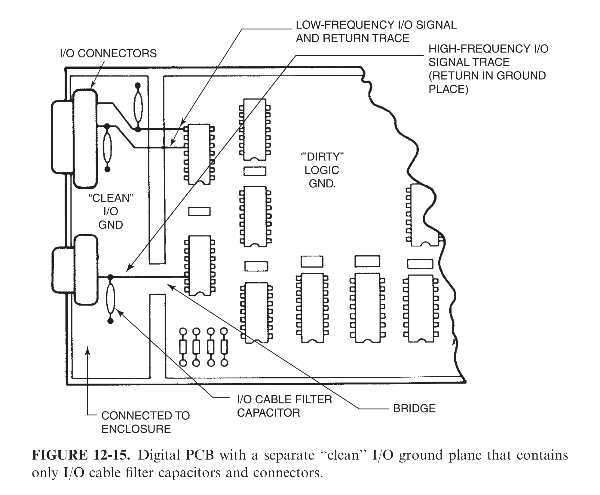
- The dirty logic ground is something he describes as the ground where all IC's are connected - for example, all decoupling capacitors are directly punched to the GND plane, causing offset voltage which excites all cables attached to the board.
- Therefore, to prevent this from happening, he then suggests all input cables be connected to something he calls "clean" I/O GND. This is the GND where the shield/metallic enclosure should be connected through a low-impedance connection as well.
- High-speed signals(higher than 5-10MHz) going to connectors should be routed through the narrow plane bridge. Low-speed signals(lower than 5MHz) should be routed on top of the plane slot with the return signal being routed on the same layer next to it - companion trace being the return path rather than the plane.
- Low impedance connection between clean ground and shield/enclosure is something he states is a clear must, due to obvious reasons. All traces shall as well be decoupled to the clean I/O GND using ceramic capacitors before leaving the board - this act as a shunt for all common mode ground current.
- All clear for me so far, the part I don't get is:
- - can this approach work in a plastic enclosure, without having the shield?
- - how to correctly size and calculate the value of the capacitance? My gut feeling tells me around 100pF/0402 or similar small size/low inductance could do it
- -----
- >@AndyAka
- ... so, which is it; RF radiated emissions or cable-conducted emissions?
- Potential failing of radiated emissions due to the ground plane offset voltage causing common-mode current to flow through the cables once when attached to the board. This would almost certainly mean conducted emission failure as well, but that is not the direct scope of the question.
- > @NickAlexeev...What type of high frequency signal have you got (frequency range differential or single-ended)? What kind of cable and connector have you got? Which EMC standard do you need to comply with (e.g. CISPR 11 class B) ?
- The question was more conceptual - most of the devices I design don't end up in metallic enclosures and are almost always without shielded connectors. I don't go higher than ethernet or USB2.0 in terms of what ends up on cables - not on standard connectors --> product requirements. There is almost always a buck converter 20W-30W, switching in the 100kHz-1MHz range - even with only this on board, and a relatively low-speed differential bus(CAN at 100kBit) there could be a radiated emission issue after cables attached if the switcher layout is poor("dirty" loop currents flowing through the ground plane)
#1: Initial revision
by
2kind
·
2022-11-25T20:43:04Z (over 2 years ago)
Minimizing Common Mode Radiation - Separating Grounds
There are various different methods to keep common mode currents off the cables, one of them being discussed on the site [here](https://electrical.codidact.com/posts/278456) and with Olin's decoupling caps post on StackExchange. Slight digression - this is for some reason, extremely hard to comprehend to 9/10 engineers. One of the approaches Henry Ott recommends in his Electromagnetic Compatibility Engineering (2009) is given on the image below:  The dirty logic ground is something he describes as the ground where all IC's are connected - for example, all decoupling capacitors are directly punched to the GND plane, causing offset voltage which excites all cables attached to the board. Therefore, to prevent this from happening, he then suggests all input cables be connected to something he calls "clean" I/O GND. This is the GND where the shield/metallic enclosure should be connected through a low-impedance connection as well. High-speed signals(higher than 5-10MHz) going to connectors should be routed through the narrow plane bridge. Low-speed signals(lower than 5MHz) should be routed on top of the plane slot with the return signal being routed on the same layer next to it - companion trace being the return path rather than the plane. Low impedance connection between clean ground and shield/enclosure is something he states is a clear must, due to obvious reasons. All traces shall as well be decoupled to the clean I/O GND using ceramic capacitors before leaving the board - this act as a shunt for all common mode ground current. All clear for me so far, the part I don't get is: - can this approach work in a plastic enclosure, without having the shield? - how to correctly size and calculate the value of the capacitance? My gut feeling tells me around 100pF/0402 or similar small size/low inductance could do it