Post History
To understand the timing, you must understand the cause. Delay is the time from input to output It is measured from +10% of input to 90% of output ( or a 10% change in output), unlike logic chips ...
#2: Post edited
by
 TonyStewart
·
2022-12-02T01:03:24Z (over 2 years ago)
TonyStewart
·
2022-12-02T01:03:24Z (over 2 years ago)
- To understand the timing, you must understand the cause.
- **Delay is the time from input to output** It is measured from +10% of input to 90% of output ( or a 10% change in output), unlike logic chips where the same voltage is used for input and output so delay is measured at Vdd/2 or 50% from input to output.
- **Rise/Fall time is just the transition time of any signal from 10% to 90%.**
- The output On-time (falling Vd, rising Id) depends on Rdson and Coss plus any load pF. The Off-time (rising Vd for Nch) depends on load R and Coss.
- Delay time is measured from 10% of the input Vgs which must exceed the threshold **V**gs(th) {aka Vt} by around +100% or 2*Vt to create an Rdon that will conduct current in the 12 Ohm pull-up from Vd to Vdd to pull down the voltage 10%.
- ` This causes the delay time to reach a condition threshold for current conduction. Vgs(th) is a leakage threshold defined in the datasheet as Vgs(th) @ Id = 250 μA and not where it will conduct Amps of current. Id=beta(Vgs-Vt)
- `
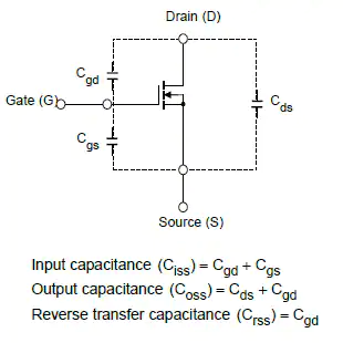
- Meanwhile, the threshold Vt can be anywhere from 2 to 5V. The drive level is unlikely to reach that threshold in the same time with a driver Ron and input capacitance Ciss.
- The output rise/fall times depend on the device Coss which increases with lower RdsOn for all FETs with a figure of merit (FoM) being RdsOn* Coss=T
- So you can always expect the delays to be asymmetrical for both delay and rise/fall time.
- Electrical characteristics of MOSFETs
- -
- [(Dynamic Characteristics Ciss/Crss/Coss) ](https://toshiba.semicon-storage.com/ap-en/semiconductor/knowledge/faq/mosfet/electrical-characteristics-of-mosfetsdynamic-characteristics-cis.html)
- -
- 
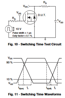
- Not shown is the driver Ron , test load Rd=13 ohms and internal inductance Ld= 6 nH, Ls=13 nH which adds further time delay and transition delay.
- In power half/full bridges _unlike logic ICs,_ cross-conduction is a short-circuit across the supply and not allowed, as this would exceed the do not exceed ratings even for a high-power FET.
- The usual method of proper design is to choose a dead-time suitable for the switching times and the load. A simple way is to use a diode to make a differential "dead time" between rise and fall. A slower RC turn-ON time and a faster turn OFF time might ensure a tri-state open circuit but then you expect a high current flyback voltage which needs to be clamped to the opposite rail.
- IC's might use a more precise way of creating a guaranteed dead time suitable for the recommended FET drivers.
- This might typically range from 0.5us to a few us depending on the storage current time constant. T=RC or or T=L/R approximately for 64%.
- In a logic IC, there is an overlap or transition current-surge between power and ground from the complementary FET output which is like a "half-bridge FET" circuit, but it is current-limited by design by the choice of RdsOn and thresholds. This is why low ESR capacitance decoupling near each CMOS IC is so important to minimize load-regulated supply noise. It varies with logic families and Vdd but might be equivalent to about 20pF and 22 to 66 ohms impedance during each transition.
- **This ought to raise more questions but I hope you at least understand how to measure and what causes delay and rise/fall time.**
- To understand the timing, you must understand the cause.
- **Delay is the time from input to output** It is measured from +10% of input to 90% of output ( or a 10% change in output), unlike logic chips where the same voltage is used for input and output so delay is measured at Vdd/2 or 50% from input to output.
- **Rise/Fall time is just the transition time of any signal from 10% to 90%.**
- 
- The output On-time (falling Vd, rising Id) depends on Rdson and Coss plus any load pF. The Off-time (rising Vd for Nch) depends on load R and Coss.
- Delay time is measured from 10% of the input Vgs which must exceed the threshold **V**gs(th) {aka Vt} by around +100% or 2*Vt to create an Rdon that will conduct current in the 12 Ohm pull-up from Vd to Vdd to pull down the voltage 10%.
- ` This causes the delay time to reach a condition threshold for current conduction. Vgs(th) is a leakage threshold defined in the datasheet as Vgs(th) @ Id = 250 μA and not where it will conduct Amps of current. Id=beta(Vgs-Vt)
- `
- Meanwhile, the threshold Vt can be anywhere from 2 to 5V. The drive level is unlikely to reach that threshold in the same time with a driver Ron and input capacitance Ciss.
- The output rise/fall times depend on the device Coss which increases with lower RdsOn for all FETs with a figure of merit (FoM) being RdsOn* Coss=T
- So you can always expect the delays to be asymmetrical for both delay and rise/fall time.
- Electrical characteristics of MOSFETs
- -
- [(Dynamic Characteristics Ciss/Crss/Coss) ](https://toshiba.semicon-storage.com/ap-en/semiconductor/knowledge/faq/mosfet/electrical-characteristics-of-mosfetsdynamic-characteristics-cis.html)
- -
- 
- Not shown is the driver Ron , test load Rd=13 ohms and internal inductance Ld= 6 nH, Ls=13 nH which adds further time delay and transition delay.
- In power half/full bridges _unlike logic ICs,_ cross-conduction is a short-circuit across the supply and not allowed, as this would exceed the do not exceed ratings even for a high-power FET.
- The usual method of proper design is to choose a dead-time suitable for the switching times and the load. A simple way is to use a diode to make a differential "dead time" between rise and fall. A slower RC turn-ON time and a faster turn OFF time might ensure a tri-state open circuit but then you expect a high current flyback voltage which needs to be clamped to the opposite rail.
- IC's might use a more precise way of creating a guaranteed dead time suitable for the recommended FET drivers.
- This might typically range from 0.5us to a few us depending on the storage current time constant. T=RC or or T=L/R approximately for 64%.
- In a logic IC, there is an overlap or transition current-surge between power and ground from the complementary FET output which is like a "half-bridge FET" circuit, but it is current-limited by design by the choice of RdsOn and thresholds. This is why low ESR capacitance decoupling near each CMOS IC is so important to minimize load-regulated supply noise. It varies with logic families and Vdd but might be equivalent to about 20pF and 22 to 66 ohms impedance during each transition.
- **This ought to raise more questions but I hope you at least understand how to measure and what causes delay and rise/fall time.**
#1: Initial revision
by
TonyStewart
·
2022-12-02T01:00:14Z (over 2 years ago)
To understand the timing, you must understand the cause.
**Delay is the time from input to output** It is measured from +10% of input to 90% of output ( or a 10% change in output), unlike logic chips where the same voltage is used for input and output so delay is measured at Vdd/2 or 50% from input to output.
**Rise/Fall time is just the transition time of any signal from 10% to 90%.**
The output On-time (falling Vd, rising Id) depends on Rdson and Coss plus any load pF. The Off-time (rising Vd for Nch) depends on load R and Coss.
Delay time is measured from 10% of the input Vgs which must exceed the threshold **V**gs(th) {aka Vt} by around +100% or 2*Vt to create an Rdon that will conduct current in the 12 Ohm pull-up from Vd to Vdd to pull down the voltage 10%.
` This causes the delay time to reach a condition threshold for current conduction. Vgs(th) is a leakage threshold defined in the datasheet as Vgs(th) @ Id = 250 μA and not where it will conduct Amps of current. Id=beta(Vgs-Vt)
`
Meanwhile, the threshold Vt can be anywhere from 2 to 5V. The drive level is unlikely to reach that threshold in the same time with a driver Ron and input capacitance Ciss.
The output rise/fall times depend on the device Coss which increases with lower RdsOn for all FETs with a figure of merit (FoM) being RdsOn* Coss=T
So you can always expect the delays to be asymmetrical for both delay and rise/fall time.
Electrical characteristics of MOSFETs
-
[(Dynamic Characteristics Ciss/Crss/Coss) ](https://toshiba.semicon-storage.com/ap-en/semiconductor/knowledge/faq/mosfet/electrical-characteristics-of-mosfetsdynamic-characteristics-cis.html)
-

Not shown is the driver Ron , test load Rd=13 ohms and internal inductance Ld= 6 nH, Ls=13 nH which adds further time delay and transition delay.
In power half/full bridges _unlike logic ICs,_ cross-conduction is a short-circuit across the supply and not allowed, as this would exceed the do not exceed ratings even for a high-power FET.
The usual method of proper design is to choose a dead-time suitable for the switching times and the load. A simple way is to use a diode to make a differential "dead time" between rise and fall. A slower RC turn-ON time and a faster turn OFF time might ensure a tri-state open circuit but then you expect a high current flyback voltage which needs to be clamped to the opposite rail.
IC's might use a more precise way of creating a guaranteed dead time suitable for the recommended FET drivers.
This might typically range from 0.5us to a few us depending on the storage current time constant. T=RC or or T=L/R approximately for 64%.
In a logic IC, there is an overlap or transition current-surge between power and ground from the complementary FET output which is like a "half-bridge FET" circuit, but it is current-limited by design by the choice of RdsOn and thresholds. This is why low ESR capacitance decoupling near each CMOS IC is so important to minimize load-regulated supply noise. It varies with logic families and Vdd but might be equivalent to about 20pF and 22 to 66 ohms impedance during each transition.
**This ought to raise more questions but I hope you at least understand how to measure and what causes delay and rise/fall time.**