What is the difference between rise/fall time and Turn-On/off Delay Time?
Hi guys so recently i was looking for a mosfet and a gate drivers and between a lot of their specification the rise/fall time and Turn-On/off Delay Time sometime it called propagation.
My questions is what is the difference between them? And how does this affect the signals or just the switching?and my last question what is the perfect proportion between them should they be the same maybe?
Thank you.
Edit:
Some explanation is needed here, so to drive a mosfet we need a PWM source and a gate driver in case if the potential source is low or if we are driving multiple mosfets like in case of H-bridge. Now the complexity begins when we try to put all that together "Synchronisation" so we have to choose well and specially when we deal with a high frequencies and to do that we need to have a good understanding of some timing specs.
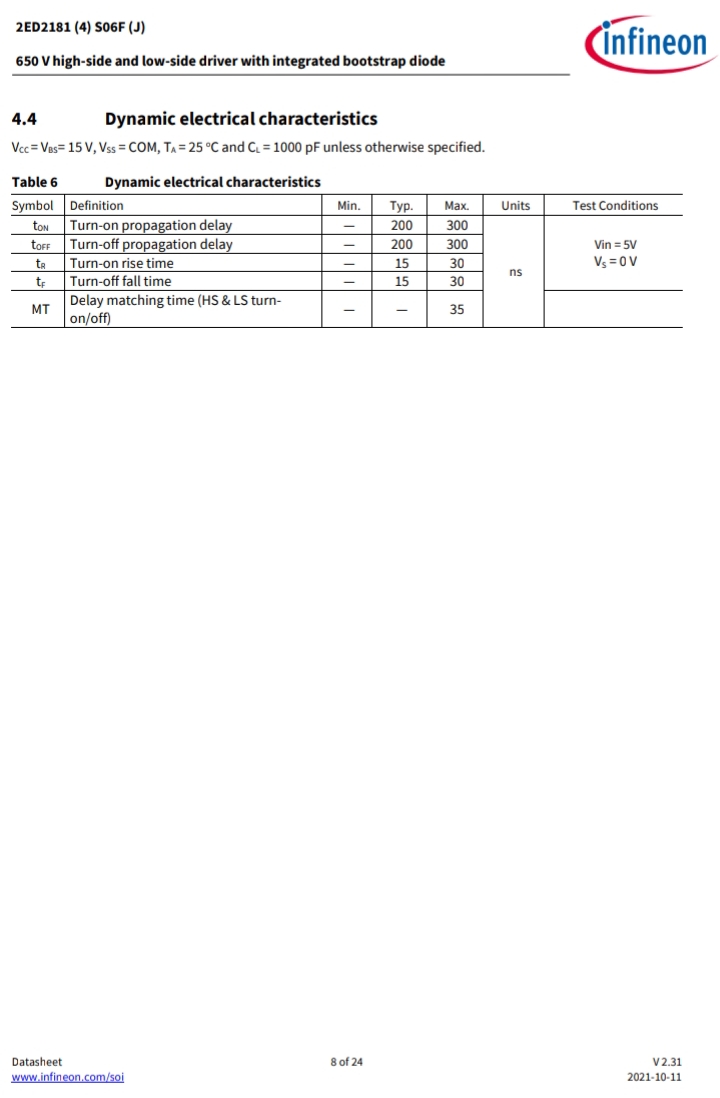
Here an example of some specs of mosfets and gate drivers:
Edit 2:
" In general, the on/off delay is how long it takes from changing the input until the output starts to do something. "
Very clear so the ON/OFF DELAY its the time that the FET driver or the mosfet take to replicate the input signal and the RISE/FALL time is the time that it take to change from the ON state to the OFF state and vice versa.
That drive me to ask another question,
It's okay that the input and the output have a delay ON/OFF time as long as the ON is equal to the OFF time, but what happen if they are not equal?
Another question about the RISE/FALL time, which is the more important as Mr. Olin mentioned in his answer, the lower it take the better, less power losses and heat to disipitate. So the RISE/FALL time should be identical to the input and must not be higher, but what happens if it is lower than the input? For example the RISE/FALL time of the input is 15ns/15ns respectivly and the output can be 10ns/10ns in the datasheet.
2 answers
You are accessing this answer with a direct link, so it's being shown above all other answers regardless of its score. You can return to the normal view.
To understand the timing, you must understand the cause.
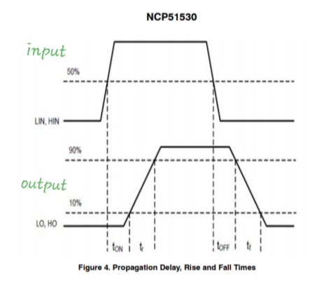
Delay is the time from input to output It is measured from +10% of input to 90% of output ( or a 10% change in output), unlike logic chips where the same voltage is used for input and output so delay is measured at Vdd/2 or 50% from input to output.
Rise/Fall time is just the transition time of any signal from 10% to 90%.
The output On-time (falling Vd, rising Id) depends on Rdson and Coss plus any load pF. The Off-time (rising Vd for Nch) depends on load R and Coss.
Delay time is measured from 10% of the input Vgs which must exceed the threshold Vgs(th) {aka Vt} by around +100% or 2*Vt to create an Rdon that will conduct current in the 12 Ohm pull-up from Vd to Vdd to pull down the voltage 10%.
This causes the delay time to reach a condition threshold for current conduction. Vgs(th) is a leakage threshold defined in the datasheet as Vgs(th) @ Id = 250 μA and not where it will conduct Amps of current. Id=beta(Vgs-Vt)
Meanwhile, the threshold Vt can be anywhere from 2 to 5V. The drive level is unlikely to reach that threshold in the same time with a driver Ron and input capacitance Ciss.
The output rise/fall times depend on the device Coss which increases with lower RdsOn for all FETs with a figure of merit (FoM) being RdsOn* Coss=T
So you can always expect the delays to be asymmetrical for both delay and rise/fall time.
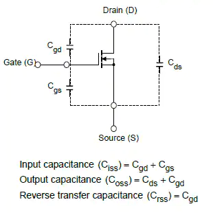
Electrical characteristics of MOSFETs
(Dynamic Characteristics Ciss/Crss/Coss)
Not shown is the driver Ron , test load Rd=13 ohms and internal inductance Ld= 6 nH, Ls=13 nH which adds further time delay and transition delay.
In power half/full bridges unlike logic ICs, cross-conduction is a short-circuit across the supply and not allowed, as this would exceed the do not exceed ratings even for a high-power FET.
The usual method of proper design is to choose a dead-time suitable for the switching times and the load. A simple way is to use a diode to make a differential "dead time" between rise and fall. A slower RC turn-ON time and a faster turn OFF time might ensure a tri-state open circuit but then you expect a high current flyback voltage which needs to be clamped to the opposite rail.
IC's might use a more precise way of creating a guaranteed dead time suitable for the recommended FET drivers.
This might typically range from 0.5us to a few us depending on the storage current time constant. T=RC or or T=L/R approximately for 64%.
In a logic IC, there is an overlap or transition current-surge between power and ground from the complementary FET output which is like a "half-bridge FET" circuit, but it is current-limited by design by the choice of RdsOn and thresholds. This is why low ESR capacitance decoupling near each CMOS IC is so important to minimize load-regulated supply noise. It varies with logic families and Vdd but might be equivalent to about 20pF and 22 to 66 ohms impedance during each transition.
This ought to raise more questions but I hope you at least understand how to measure and what causes delay and rise/fall time.
In general, the on/off delay is how long it takes from changing the input until the output starts to do something. The rise/fall time is how long it takes to do the something, once it starts doing it.
Your first FET driver datasheet is a good example:
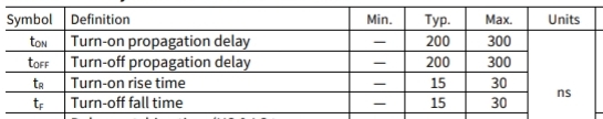
The switching characteristics are idealized as up to 300 ns where nothing happens after you change the input, then another 30 ns for the output to transition on/off or off/on once it starts doing something. The total worst case time from switching the input until the output is fully in its new state is therefore 330 ns.
So why would anyone care about the details and not just the overall 330 ns delay? Because sometimes the overall delay isn't as important as a fast transition. An ideal switch dissipates no power when off because the current is zero, and no power when on because the voltage across it is zero. The power dissipated in-between can be significant. You want to have the FET transition thru the in-between region as fast as possible.
This FET driver guarantees that it won't leave the FET gate in the in-between region for more than 30 ns each transition. If you're switching a high power heater, for example, the 330 ns delay from when the thermostat says to switch until the load is actually switched is inconsequential. However, transitioning the FET quickly can be the difference between requiring a heat sink or not.
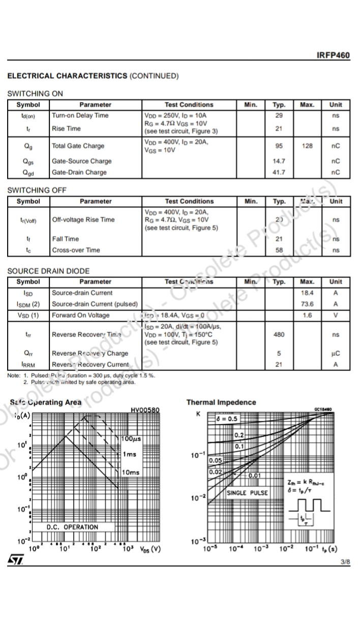
The specs for a FET are interpreted similarly:
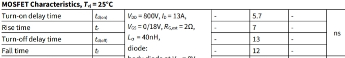
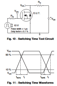
The delay time in this case is how long it takes for the channel to change its conduction characteristics from a gate voltage change.
The rise and fall times is how long it takes for the drain voltage to change in a particular circuit. Note how it explicitly says the off/on gate voltages are 0 and 18 V, and that the load on the drain is 2 Ω. These are probably the conditions under which the manufacturer knows the response will be fastest.

0 comment threads