Post History
I am an electrical engineering student and I just finished designing an ECG-amplifier circuit. Here is the schematic: - It is fairly simple. Initially, there is a 1st order highpass filter. Then...
#4: Post edited
by
 Carl
·
2023-03-31T12:05:10Z (about 2 years ago)
Carl
·
2023-03-31T12:05:10Z (about 2 years ago)
- I am an electrical engineering student and I just finished designing an ECG-amplifier circuit. Here is the schematic: -
- 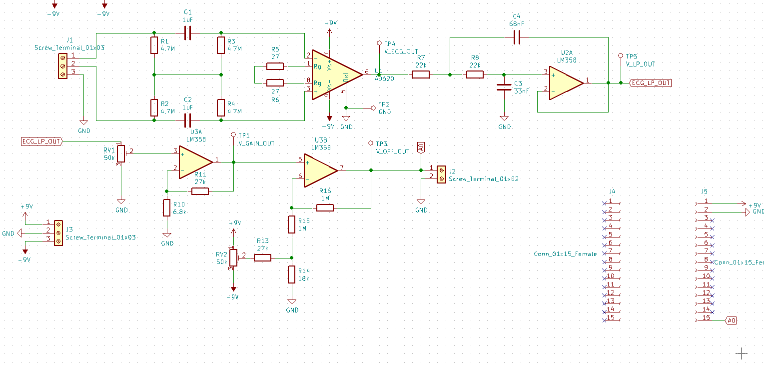
- It is fairly simple. Initially, there is a 1st order highpass filter. Then, a differential amplification stage with AD620N in-amp followed by a Sallen-Key 2nd order lowpass filter. Finally, a gain and offset stage. The two female pin-header connectors (J4 and J5) are for plugging in an esp8266 module to sample the processed signal with its ADC. There are also some test points and some screw terminals.
- I have also designed and ordered a PCB for this circuit here:
- 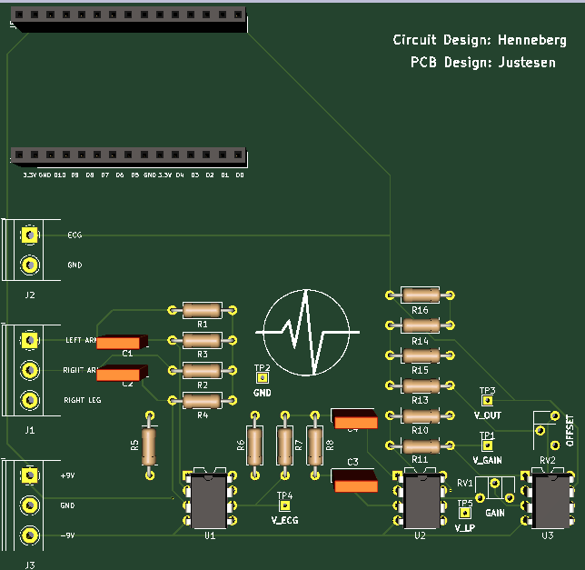
- The PCB is 100x100mm, has 2 layers, and it only uses THT-components. The +9V and -9V are connected through traces to the amplifiers, and I use 1 GND plane.
**Questions**: I'm new to PCB-design and I don't have a feeling for what a "good" design is. Have I made some big "no-nos"? Is there a standard for placing components that's a good idea to follow? Where is it a good place to start with the PCB-design? Should I go from left to right following my schematic and wire components accordingly? Is this a poor design?
- I am an electrical engineering student and I just finished designing an ECG-amplifier circuit. Here is the schematic: -
- 
- It is fairly simple. Initially, there is a 1st order highpass filter. Then, a differential amplification stage with AD620N in-amp followed by a Sallen-Key 2nd order lowpass filter. Finally, a gain and offset stage. The two female pin-header connectors (J4 and J5) are for plugging in an esp8266 module to sample the processed signal with its ADC. There are also some test points and some screw terminals.
- I have also designed and ordered a PCB for this circuit here:
- 
- The PCB is 100x100mm, has 2 layers, and it only uses THT-components. The +9V and -9V are connected through traces to the amplifiers, and I use 1 GND plane.
- **Questions**: I'm new to PCB-design and I don't have a feeling for what a "good" design is. Have I made some big "no-nos"? Is there a standard for placing components that's a good idea to follow? Where is it a good place to start with the PCB-design? Should I go from left to right following my schematic and wire components accordingly (that's what I have done)? Is this a poor design?
#3: Post edited
by
Carl
·
2023-03-31T11:52:54Z (about 2 years ago)
- I am an electrical engineering student and I just finished designing an ECG-amplifier circuit. Here is the schematic: -
- 
It is fairly simple. Initially, there is a 1st order highpass filter. THen, a differential amplification stage with AD620N in-amp followed by a Sallen-Key 2nd order lowpass filter. Finally, a gain and offset stage. The two female pin-header connectors (J4 and J5) are for plugging in an esp8266 module to sample the processed signal with its ADC. There are also some test points and some screw terminals.- I have also designed and ordered a PCB for this circuit here:
- 
- The PCB is 100x100mm, has 2 layers, and it only uses THT-components. The +9V and -9V are connected through traces to the amplifiers, and I use 1 GND plane.
- **Questions**: I'm new to PCB-design and I don't have a feeling for what a "good" design is. Have I made some big "no-nos"? Is there a standard for placing components that's a good idea to follow? Where is it a good place to start with the PCB-design? Should I go from left to right following my schematic and wire components accordingly? Is this a poor design?
- I am an electrical engineering student and I just finished designing an ECG-amplifier circuit. Here is the schematic: -
- 
- It is fairly simple. Initially, there is a 1st order highpass filter. Then, a differential amplification stage with AD620N in-amp followed by a Sallen-Key 2nd order lowpass filter. Finally, a gain and offset stage. The two female pin-header connectors (J4 and J5) are for plugging in an esp8266 module to sample the processed signal with its ADC. There are also some test points and some screw terminals.
- I have also designed and ordered a PCB for this circuit here:
- 
- The PCB is 100x100mm, has 2 layers, and it only uses THT-components. The +9V and -9V are connected through traces to the amplifiers, and I use 1 GND plane.
- **Questions**: I'm new to PCB-design and I don't have a feeling for what a "good" design is. Have I made some big "no-nos"? Is there a standard for placing components that's a good idea to follow? Where is it a good place to start with the PCB-design? Should I go from left to right following my schematic and wire components accordingly? Is this a poor design?
#2: Post edited
by
Carl
·
2023-03-31T11:18:37Z (about 2 years ago)
- I am an electrical engineering student and I just finished designing an ECG-amplifier circuit. Here is the schematic: -
- 
It is fairly simple. A differential amplification stage using the AD620N in-amp followed by a Sallen-Key 2nd order lowpass filter. And finally a gain and offset stage. The two female pin-header connectors (J4 and J5) are for plugging in an esp8266 module to sample the processed signal with its ADC. There are also some test points and some screw terminals.- I have also designed and ordered a PCB for this circuit here:
- 
- The PCB is 100x100mm, has 2 layers, and it only uses THT-components. The +9V and -9V are connected through traces to the amplifiers, and I use 1 GND plane.
- **Questions**: I'm new to PCB-design and I don't have a feeling for what a "good" design is. Have I made some big "no-nos"? Is there a standard for placing components that's a good idea to follow? Where is it a good place to start with the PCB-design? Should I go from left to right following my schematic and wire components accordingly? Is this a poor design?
- I am an electrical engineering student and I just finished designing an ECG-amplifier circuit. Here is the schematic: -
- 
- It is fairly simple. Initially, there is a 1st order highpass filter. THen, a differential amplification stage with AD620N in-amp followed by a Sallen-Key 2nd order lowpass filter. Finally, a gain and offset stage. The two female pin-header connectors (J4 and J5) are for plugging in an esp8266 module to sample the processed signal with its ADC. There are also some test points and some screw terminals.
- I have also designed and ordered a PCB for this circuit here:
- 
- The PCB is 100x100mm, has 2 layers, and it only uses THT-components. The +9V and -9V are connected through traces to the amplifiers, and I use 1 GND plane.
- **Questions**: I'm new to PCB-design and I don't have a feeling for what a "good" design is. Have I made some big "no-nos"? Is there a standard for placing components that's a good idea to follow? Where is it a good place to start with the PCB-design? Should I go from left to right following my schematic and wire components accordingly? Is this a poor design?
#1: Initial revision
by
Carl
·
2023-03-31T11:09:44Z (about 2 years ago)
What is a good PCB-layout?
I am an electrical engineering student and I just finished designing an ECG-amplifier circuit. Here is the schematic: -  It is fairly simple. A differential amplification stage using the AD620N in-amp followed by a Sallen-Key 2nd order lowpass filter. And finally a gain and offset stage. The two female pin-header connectors (J4 and J5) are for plugging in an esp8266 module to sample the processed signal with its ADC. There are also some test points and some screw terminals. I have also designed and ordered a PCB for this circuit here:  The PCB is 100x100mm, has 2 layers, and it only uses THT-components. The +9V and -9V are connected through traces to the amplifiers, and I use 1 GND plane. **Questions**: I'm new to PCB-design and I don't have a feeling for what a "good" design is. Have I made some big "no-nos"? Is there a standard for placing components that's a good idea to follow? Where is it a good place to start with the PCB-design? Should I go from left to right following my schematic and wire components accordingly? Is this a poor design?