Post History
I'm designing a board that contains a cortex-M4 mcu working at 120MHz, and an ethernet bus with a wiznet chip that communicates with SPI. The ethernet chip gives me a phy output that goes directly...
#7: Post edited
by
 Lorenzo Donati
·
2023-08-12T15:28:06Z (almost 2 years ago)
Lorenzo Donati
·
2023-08-12T15:28:06Z (almost 2 years ago)
Retagged.
#6: Post edited
by
 DeadMouse
·
2023-06-29T18:20:25Z (almost 2 years ago)
DeadMouse
·
2023-06-29T18:20:25Z (almost 2 years ago)
- I'm designing a board that contains a cortex-M4 mcu working at 120MHz, and an ethernet bus with a wiznet chip that communicates with SPI.
- The ethernet chip gives me a phy output that goes directly to a connector with internal magnetics.
- All circuits are powered by a DC to DC buck converter.
- The final product is a 4-layer board.
- The stackup is:
- Signals
- Ground
- Power
- Signals
- The board is one sided (every component is placed at the top layer).
- All the traces are nicely routed on top with about 10 percent of them are at the bottom.
- The inner ground layer is consistent across the whole board and it is not interrupted anywhere.
- Every trace or pad that needs ground goes through a via to this layer.
- The same happens with the power planes.
- This is to minimise impedance.
- The size of the board is 130mmx90mm.
- The final step is whether I need to fill the empty space of the rest of the board (top and bottom) with coper ground pour (that will stitched to ground) or not.
- I read that it is usually not needed in multilayer boards. However it is mostly useful to help manufacturers as it reduces etching time, less chemical waste, easier to manufacture etc.
- Also, it reduces the twisting which is more useful in large PCBs although I'm not sure if my board is considered large. probably not.
- Personally I'd like to leave it as it is without any ground pour on the outer layers but I'm concerned about manufacturability.
- On the other hand if I try to fill the board will ground pour I'll have to stich it with vias that will probably need careful consideration on the placement.
- What do we do in those cases?
- Would it be better to have some lands of copper that is stitched well to the ground but not connected to any components pads?
- Regarding the grounding of the bypass capacitors:
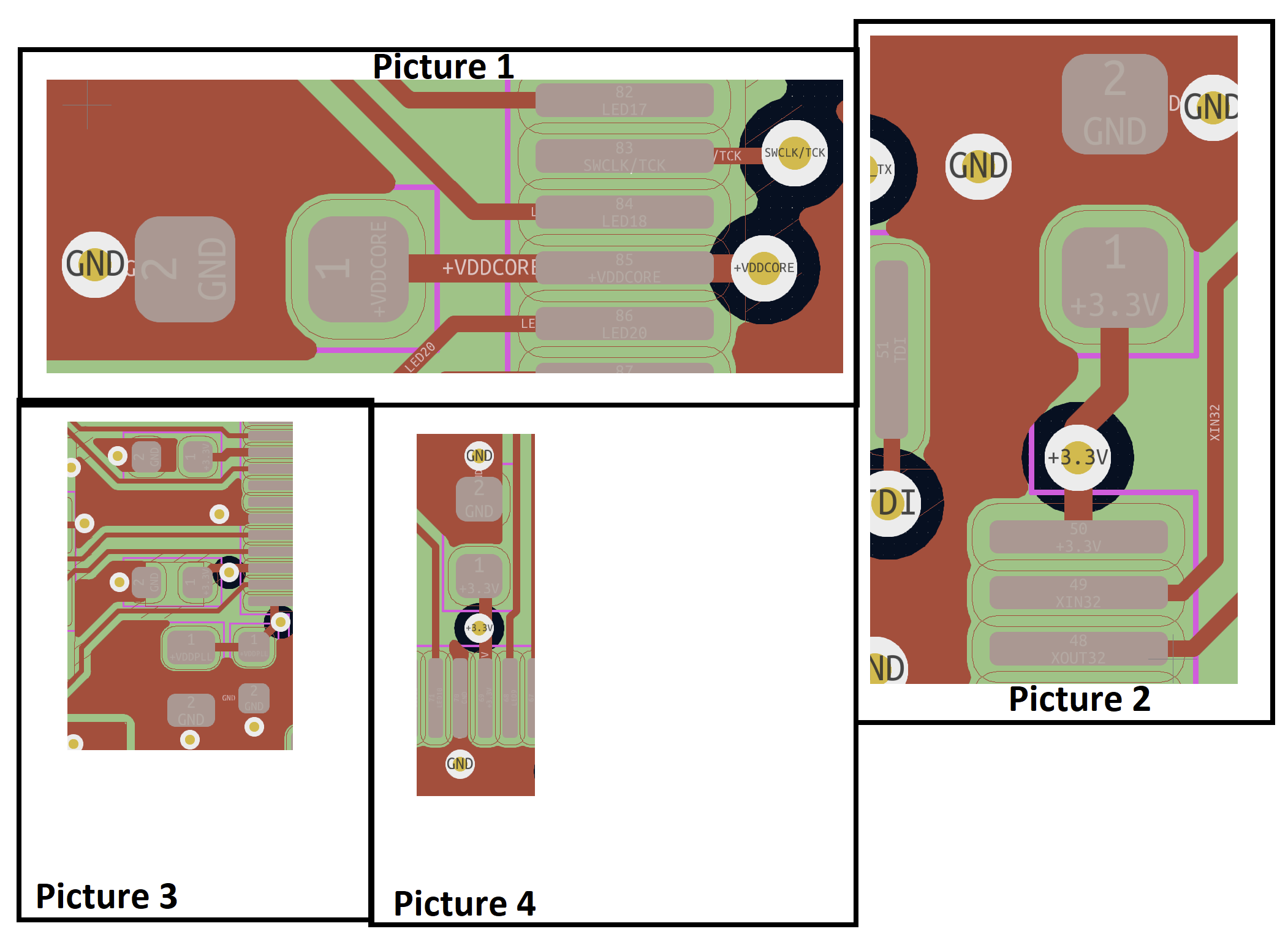
- I'm posting a screenshot of how these capacitors are connected to the ground plane.
 
- I'm designing a board that contains a cortex-M4 mcu working at 120MHz, and an ethernet bus with a wiznet chip that communicates with SPI.
- The ethernet chip gives me a phy output that goes directly to a connector with internal magnetics.
- All circuits are powered by a DC to DC buck converter.
- The final product is a 4-layer board.
- The stackup is:
- Signals
- Ground
- Power
- Signals
- The board is one sided (every component is placed at the top layer).
- All the traces are nicely routed on top with about 10 percent of them are at the bottom.
- The inner ground layer is consistent across the whole board and it is not interrupted anywhere.
- Every trace or pad that needs ground goes through a via to this layer.
- The same happens with the power planes.
- This is to minimise impedance.
- The size of the board is 130mmx90mm.
- The final step is whether I need to fill the empty space of the rest of the board (top and bottom) with coper ground pour (that will stitched to ground) or not.
- I read that it is usually not needed in multilayer boards. However it is mostly useful to help manufacturers as it reduces etching time, less chemical waste, easier to manufacture etc.
- Also, it reduces the twisting which is more useful in large PCBs although I'm not sure if my board is considered large. probably not.
- Personally I'd like to leave it as it is without any ground pour on the outer layers but I'm concerned about manufacturability.
- On the other hand if I try to fill the board will ground pour I'll have to stich it with vias that will probably need careful consideration on the placement.
- What do we do in those cases?
- Would it be better to have some lands of copper that is stitched well to the ground but not connected to any components pads?
- Regarding the grounding of the bypass capacitors:
- I'm posting a screenshot of how these capacitors are connected to the ground plane.
- 
#5: Post edited
by
DeadMouse
·
2023-06-29T18:15:13Z (almost 2 years ago)
- I'm designing a board that contains a cortex-M4 mcu working at 120MHz, and an ethernet bus with a wiznet chip that communicates with SPI.
- The ethernet chip gives me a phy output that goes directly to a connector with internal magnetics.
- All circuits are powered by a DC to DC buck converter.
- The final product is a 4-layer board.
- The stackup is:
- Signals
- Ground
- Power
- Signals
- The board is one sided (every component is placed at the top layer).
- All the traces are nicely routed on top with about 10 percent of them are at the bottom.
- The inner ground layer is consistent across the whole board and it is not interrupted anywhere.
- Every trace or pad that needs ground goes through a via to this layer.
- The same happens with the power planes.
- This is to minimise impedance.
- The size of the board is 130mmx90mm.
- The final step is whether I need to fill the empty space of the rest of the board (top and bottom) with coper ground pour (that will stitched to ground) or not.
- I read that it is usually not needed in multilayer boards. However it is mostly useful to help manufacturers as it reduces etching time, less chemical waste, easier to manufacture etc.
- Also, it reduces the twisting which is more useful in large PCBs although I'm not sure if my board is considered large. probably not.
- Personally I'd like to leave it as it is without any ground pour on the outer layers but I'm concerned about manufacturability.
- On the other hand if I try to fill the board will ground pour I'll have to stich it with vias that will probably need careful consideration on the placement.
- What do we do in those cases?
- Would it be better to have some lands of copper that is stitched well to the ground but not connected to any components pads?
- Regarding the grounding of the bypass capacitors:
- I'm posting a screenshot of how these capacitors are connected to the ground plane.
- 
-  
- 
#4: Post edited
by
DeadMouse
·
2023-06-29T18:05:08Z (almost 2 years ago)
- I'm designing a board that contains a cortex-M4 mcu working at 120MHz, and an ethernet bus with a wiznet chip that communicates with SPI.
- The ethernet chip gives me a phy output that goes directly to a connector with internal magnetics.
- All circuits are powered by a DC to DC buck converter.
- The final product is a 4-layer board.
- The stackup is:
- Signals
- Ground
- Power
- Signals
- The board is one sided (every component is placed at the top layer).
- All the traces are nicely routed on top with about 10 percent of them are at the bottom.
- The inner ground layer is consistent across the whole board and it is not interrupted anywhere.
- Every trace or pad that needs ground goes through a via to this layer.
- The same happens with the power planes.
- This is to minimise impedance.
- The size of the board is 130mmx90mm.
- The final step is whether I need to fill the empty space of the rest of the board (top and bottom) with coper ground pour (that will stitched to ground) or not.
- I read that it is usually not needed in multilayer boards. However it is mostly useful to help manufacturers as it reduces etching time, less chemical waste, easier to manufacture etc.
- Also, it reduces the twisting which is more useful in large PCBs although I'm not sure if my board is considered large. probably not.
- Personally I'd like to leave it as it is without any ground pour on the outer layers but I'm concerned about manufacturability.
- On the other hand if I try to fill the board will ground pour I'll have to stich it with vias that will probably need careful consideration on the placement.
- What do we do in those cases?
Would it be better to have some lands of copper that is stitched well to the ground but not connected to any components pads?
- I'm designing a board that contains a cortex-M4 mcu working at 120MHz, and an ethernet bus with a wiznet chip that communicates with SPI.
- The ethernet chip gives me a phy output that goes directly to a connector with internal magnetics.
- All circuits are powered by a DC to DC buck converter.
- The final product is a 4-layer board.
- The stackup is:
- Signals
- Ground
- Power
- Signals
- The board is one sided (every component is placed at the top layer).
- All the traces are nicely routed on top with about 10 percent of them are at the bottom.
- The inner ground layer is consistent across the whole board and it is not interrupted anywhere.
- Every trace or pad that needs ground goes through a via to this layer.
- The same happens with the power planes.
- This is to minimise impedance.
- The size of the board is 130mmx90mm.
- The final step is whether I need to fill the empty space of the rest of the board (top and bottom) with coper ground pour (that will stitched to ground) or not.
- I read that it is usually not needed in multilayer boards. However it is mostly useful to help manufacturers as it reduces etching time, less chemical waste, easier to manufacture etc.
- Also, it reduces the twisting which is more useful in large PCBs although I'm not sure if my board is considered large. probably not.
- Personally I'd like to leave it as it is without any ground pour on the outer layers but I'm concerned about manufacturability.
- On the other hand if I try to fill the board will ground pour I'll have to stich it with vias that will probably need careful consideration on the placement.
- What do we do in those cases?
- Would it be better to have some lands of copper that is stitched well to the ground but not connected to any components pads?
- Regarding the grounding of the bypass capacitors:
- I'm posting a screenshot of how these capacitors are connected to the ground plane.
- 
-  
#3: Post edited
by
DeadMouse
·
2023-06-28T21:40:58Z (almost 2 years ago)
- I'm designing a board that contains a cortex-M4 mcu working at 120MHz, and an ethernet bus with a wiznet chip that communicates with SPI.
- The ethernet chip gives me a phy output that goes directly to a connector with internal magnetics.
- All circuits are powered by a DC to DC buck converter.
- The final product is a 4-layer board.
- The stackup is:
- Signals
- Ground
- Power
- Signals
- The board is one sided (every component is placed at the top layer).
- All the traces are nicely routed on top with about 10 percent of them are at the bottom.
- The inner ground layer is consistent across the whole board and it is not interrupted anywhere.
- Every trace or pad that needs ground goes through a via to this layer.
- The same happens with the power planes.
- This is to minimise impedance.
- The size of the board is 130mmx90mm.
- The final step is whether I need to fill the empty space of the rest of the board (top and bottom) with coper ground pour (that will stitched to ground) or not.
- I read that it is usually not needed in multilayer boards. However it is mostly useful to help manufacturers as it reduces etching time, less chemical waste, easier to manufacture etc.
- Also, it reduces the twisting which is more useful in large PCBs although I'm not sure if my board is considered large. probably not.
- Personally I'd like to leave it as it is without any ground pour on the outer layers but I'm concerned about manufacturability.
- On the other hand if I try to fill the board will ground pour I'll have to stich it with vias that will probably need careful consideration on the placement.
- What do we do in those cases?
Would it be better to have some lands of copper that is stitched well to the ground but not connected to any smd pads?
- I'm designing a board that contains a cortex-M4 mcu working at 120MHz, and an ethernet bus with a wiznet chip that communicates with SPI.
- The ethernet chip gives me a phy output that goes directly to a connector with internal magnetics.
- All circuits are powered by a DC to DC buck converter.
- The final product is a 4-layer board.
- The stackup is:
- Signals
- Ground
- Power
- Signals
- The board is one sided (every component is placed at the top layer).
- All the traces are nicely routed on top with about 10 percent of them are at the bottom.
- The inner ground layer is consistent across the whole board and it is not interrupted anywhere.
- Every trace or pad that needs ground goes through a via to this layer.
- The same happens with the power planes.
- This is to minimise impedance.
- The size of the board is 130mmx90mm.
- The final step is whether I need to fill the empty space of the rest of the board (top and bottom) with coper ground pour (that will stitched to ground) or not.
- I read that it is usually not needed in multilayer boards. However it is mostly useful to help manufacturers as it reduces etching time, less chemical waste, easier to manufacture etc.
- Also, it reduces the twisting which is more useful in large PCBs although I'm not sure if my board is considered large. probably not.
- Personally I'd like to leave it as it is without any ground pour on the outer layers but I'm concerned about manufacturability.
- On the other hand if I try to fill the board will ground pour I'll have to stich it with vias that will probably need careful consideration on the placement.
- What do we do in those cases?
- Would it be better to have some lands of copper that is stitched well to the ground but not connected to any components pads?
#2: Post edited
by
DeadMouse
·
2023-06-28T21:18:50Z (almost 2 years ago)
- I'm designing a board that contains a cortex-M4 mcu working at 120MHz, and an ethernet bus with a wiznet chip that communicates with SPI.
- The ethernet chip gives me a phy output that goes directly to a connector with internal magnetics.
- All circuits are powered by a DC to DC buck converter.
- The final product is a 4-layer board.
- The stackup is:
- Signals
- Ground
- Power
- Signals
- The board is one sided (every component is placed at the top layer).
- All the traces are nicely routed on top with about 10 percent of them are at the bottom.
- The inner ground layer is consistent across the whole board and it is not interrupted anywhere.
- Every trace or pad that needs ground goes through a via to this layer.
- The same happens with the power planes.
- This is to minimise impedance.
- The size of the board is 130mmx90mm.
- The final step is whether I need to fill the empty space of the rest of the board (top and bottom) with coper ground pour (that will stitched to ground) or not.
- I read that it is usually not needed in multilayer boards. However it is mostly useful to help manufacturers as it reduces etching time, less chemical waste, easier to manufacture etc.
- Also, it reduces the twisting which is more useful in large PCBs although I'm not sure if my board is considered large. probably not.
- Personally I'd like to leave it as it is without any ground pour on the outer layers but I'm concerned about manufacturability.
- On the other hand if I try to fill the board will ground pour I'll have to stich it with vias that will probably need careful consideration on the placement.
What do we do in those cases?
- I'm designing a board that contains a cortex-M4 mcu working at 120MHz, and an ethernet bus with a wiznet chip that communicates with SPI.
- The ethernet chip gives me a phy output that goes directly to a connector with internal magnetics.
- All circuits are powered by a DC to DC buck converter.
- The final product is a 4-layer board.
- The stackup is:
- Signals
- Ground
- Power
- Signals
- The board is one sided (every component is placed at the top layer).
- All the traces are nicely routed on top with about 10 percent of them are at the bottom.
- The inner ground layer is consistent across the whole board and it is not interrupted anywhere.
- Every trace or pad that needs ground goes through a via to this layer.
- The same happens with the power planes.
- This is to minimise impedance.
- The size of the board is 130mmx90mm.
- The final step is whether I need to fill the empty space of the rest of the board (top and bottom) with coper ground pour (that will stitched to ground) or not.
- I read that it is usually not needed in multilayer boards. However it is mostly useful to help manufacturers as it reduces etching time, less chemical waste, easier to manufacture etc.
- Also, it reduces the twisting which is more useful in large PCBs although I'm not sure if my board is considered large. probably not.
- Personally I'd like to leave it as it is without any ground pour on the outer layers but I'm concerned about manufacturability.
- On the other hand if I try to fill the board will ground pour I'll have to stich it with vias that will probably need careful consideration on the placement.
- What do we do in those cases?
- Would it be better to have some lands of copper that is stitched well to the ground but not connected to any smd pads?
#1: Initial revision
by
DeadMouse
·
2023-06-28T15:40:18Z (almost 2 years ago)
Ground pour on outer layers on 4-layer PCB
I'm designing a board that contains a cortex-M4 mcu working at 120MHz, and an ethernet bus with a wiznet chip that communicates with SPI.

The ethernet chip gives me a phy output that goes directly to a connector with internal magnetics.


All circuits are powered by a DC to DC buck converter.

The final product is a 4-layer board.

The stackup is:
Signals
Ground
Power
Signals

The board is one sided (every component is placed at the top layer).

All the traces are nicely routed on top with about 10 percent of them are at the bottom.

The inner ground layer is consistent across the whole board and it is not interrupted anywhere.

Every trace or pad that needs ground goes through a via to this layer.

The same happens with the power planes.

This is to minimise impedance.

The size of the board is 130mmx90mm.

The final step is whether I need to fill the empty space of the rest of the board (top and bottom) with coper ground pour (that will stitched to ground) or not.

I read that it is usually not needed in multilayer boards. However it is mostly useful to help manufacturers as it reduces etching time, less chemical waste, easier to manufacture etc.

Also, it reduces the twisting which is more useful in large PCBs although I'm not sure if my board is considered large. probably not.

Personally I'd like to leave it as it is without any ground pour on the outer layers but I'm concerned about manufacturability.

On the other hand if I try to fill the board will ground pour I'll have to stich it with vias that will probably need careful consideration on the placement.

What do we do in those cases?