Regulated charge pump design
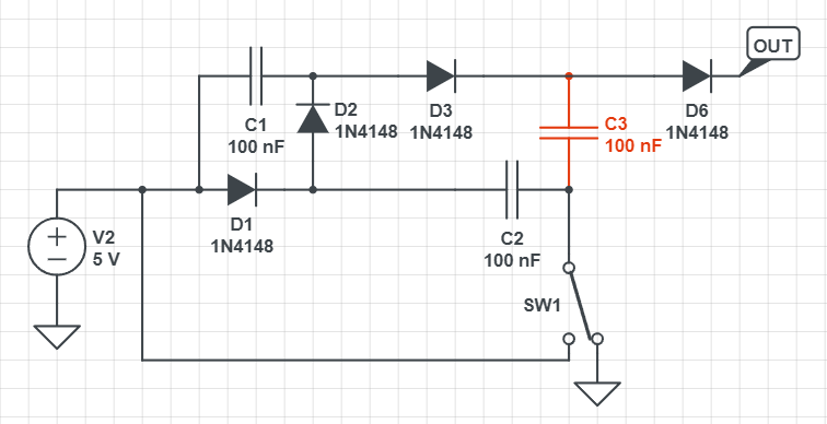
I am working with an IC that uses a partially intergrated regulated charge pump. The circuit looks like this:
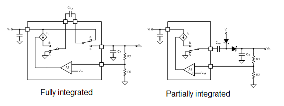
It behaves like a voltage doubler. However, when looking at other regulated charge pumps I am coming across much simpler designs such as this on for example:
I understand the wokring of a single-stage charge pump and the fact that they can be chained together. However, the circuit from the first diagram confuses me as it looks like nothing I could find online.
My questions are:
- Why are C2 and C3 connected across D2 and D3?
- What is the purpose of C1?
- What type of charge pump is this?
1 answer
That circuit is drawn rather obfuscated, but it does seem to make sense:
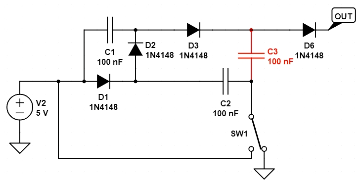
Start by looking only at D1, D2, C1, and C2. Pretend D3, C3, and D6 don't exist. Although not drawn very well, this is a basic charge pump. For simplicity, let's pretend the diodes are ideal. The actual output voltage will be lower by the series diode drops, but we don't need to take that into account to understand how the circuit works.
When SW1 is connected to ground, C2 is charged up to 5 V thru D1. When SW1 switches, the right end of C2 is connected to 5 V. That means the left end is at 10 V. After a few cycles, that charges up C1 thru D2 so that the right end if C1 is at 10 V. What you have is a classic charge pump voltage doubler, with the output being the right end of C1 (or the top end of D2).
We can now ignore how the 10 V was generated, and start with 10 V at the left end of D3. D3, C3, and D6 form another charge pump, adding 5 V to whatever is at the left end of D3. With ideal diodes, there would be spurts of 15 V squirting out the right end of D6. Assuming you don't want pulses, you'd have to put a cap to ground on the right end of D6.
You say this chip is meant to double the input voltage. Just a charge pump doubler can't actually double the voltage because of the diode drops. My guess is that this chip has a charge pump that triples the voltage (minus the diode drops), so that there is some headroom to regulate the output to a true double.
1 comment thread

0 comment threads