Post History
Mini-circuits LNA PHA-LN13+ has suggested: Eval board Layout Eval Gerber The image took from the Gerber file (3rd ref.) (Though all 3-reference mentioned containing it): There I have som...
#5: Post edited
- Mini-circuits LNA PHA-LN13+ has suggested:
- * [Eval board](https://www.minicircuits.com/pcb/WTB-969-13LN+_P02.pdf)
- * [Layout](https://www.minicircuits.com/pcb/98-pl523.pdf)
- * [Eval Gerber](https://www.minicircuits.com/gerber/TB-969-13LN+.zip)
The image took from the Gerber file (Though all 3-reference mentioned containing it):- 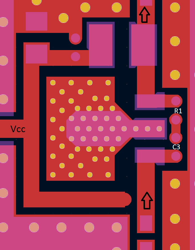
- There I have some questions:
- 1) Why Vcc has reached to near the input, The only reason I can see is to achieve more HF capacitance in Vcc but it can be achieved in other way and leave input CPW side ground being untouched. (For example, we can have larger input trace and instead remove leg which pointing toward input.)
- 2) LNA ground pad has larger gap from input and output, maybe due to reduced coupling from input to output. But if that is the case, I think the other side ground (right side of picture) must also have higher gap distance to ensure more isolation, but why doesn't that happen?
- 3) Input decoupling caps in Vcc path can be mirrored over horizontal axis to let caps benefit from local ground, but they've decided to not doing that, why?
- 4) Does the half circle in Vcc path in adjacent to input is intentional or unintentional, why it must be half circle and not 90 deg rectangular?
- 5) Am I right in all scenarios, and they've just drawn something to just get rid of finishing their product docs?
- Mini-circuits LNA PHA-LN13+ has suggested:
- * [Eval board](https://www.minicircuits.com/pcb/WTB-969-13LN+_P02.pdf)
- * [Layout](https://www.minicircuits.com/pcb/98-pl523.pdf)
- * [Eval Gerber](https://www.minicircuits.com/gerber/TB-969-13LN+.zip)
- The image took from the Gerber file (3rd ref.) (Though all 3-reference mentioned containing it):
- 
- There I have some questions:
- 1) Why Vcc has reached to near the input, The only reason I can see is to achieve more HF capacitance in Vcc but it can be achieved in other way and leave input CPW side ground being untouched. (For example, we can have larger input trace and instead remove leg which pointing toward input.)
- 2) LNA ground pad has larger gap from input and output, maybe due to reduced coupling from input to output. But if that is the case, I think the other side ground (right side of picture) must also have higher gap distance to ensure more isolation, but why doesn't that happen?
- 3) Input decoupling caps in Vcc path can be mirrored over horizontal axis to let caps benefit from local ground, but they've decided to not doing that, why?
- 4) Does the half circle in Vcc path in adjacent to input is intentional or unintentional, why it must be half circle and not 90 deg rectangular?
- 5) Am I right in all scenarios, and they've just drawn something to just get rid of finishing their product docs?
#4: Post edited
- Mini-circuits LNA PHA-LN13+ has suggested:
- * [Eval board](https://www.minicircuits.com/pcb/WTB-969-13LN+_P02.pdf)
- * [Layout](https://www.minicircuits.com/pcb/98-pl523.pdf)
- * [Eval Gerber](https://www.minicircuits.com/gerber/TB-969-13LN+.zip)
The image took from the Gerber file:- 
- There I have some questions:
- 1) Why Vcc has reached to near the input, The only reason I can see is to achieve more HF capacitance in Vcc but it can be achieved in other way and leave input CPW side ground being untouched. (For example, we can have larger input trace and instead remove leg which pointing toward input.)
- 2) LNA ground pad has larger gap from input and output, maybe due to reduced coupling from input to output. But if that is the case, I think the other side ground (right side of picture) must also have higher gap distance to ensure more isolation, but why doesn't that happen?
- 3) Input decoupling caps in Vcc path can be mirrored over horizontal axis to let caps benefit from local ground, but they've decided to not doing that, why?
- 4) Does the half circle in Vcc path in adjacent to input is intentional or unintentional, why it must be half circle and not 90 deg rectangular?
- 5) Am I right in all scenarios, and they've just drawn something to just get rid of finishing their product docs?
- Mini-circuits LNA PHA-LN13+ has suggested:
- * [Eval board](https://www.minicircuits.com/pcb/WTB-969-13LN+_P02.pdf)
- * [Layout](https://www.minicircuits.com/pcb/98-pl523.pdf)
- * [Eval Gerber](https://www.minicircuits.com/gerber/TB-969-13LN+.zip)
- The image took from the Gerber file (Though all 3-reference mentioned containing it):
- 
- There I have some questions:
- 1) Why Vcc has reached to near the input, The only reason I can see is to achieve more HF capacitance in Vcc but it can be achieved in other way and leave input CPW side ground being untouched. (For example, we can have larger input trace and instead remove leg which pointing toward input.)
- 2) LNA ground pad has larger gap from input and output, maybe due to reduced coupling from input to output. But if that is the case, I think the other side ground (right side of picture) must also have higher gap distance to ensure more isolation, but why doesn't that happen?
- 3) Input decoupling caps in Vcc path can be mirrored over horizontal axis to let caps benefit from local ground, but they've decided to not doing that, why?
- 4) Does the half circle in Vcc path in adjacent to input is intentional or unintentional, why it must be half circle and not 90 deg rectangular?
- 5) Am I right in all scenarios, and they've just drawn something to just get rid of finishing their product docs?
#3: Post edited
Mini-circuits LNA PHA-LN13+ has suggested a [layout ](https://www.minicircuits.com/pcb/WTB-969-13LN+_P02.pdf)for it:- 
- There I have some questions:
- 1) Why Vcc has reached to near the input, The only reason I can see is to achieve more HF capacitance in Vcc but it can be achieved in other way and leave input CPW side ground being untouched. (For example, we can have larger input trace and instead remove leg which pointing toward input.)
- 2) LNA ground pad has larger gap from input and output, maybe due to reduced coupling from input to output. But if that is the case, I think the other side ground (right side of picture) must also have higher gap distance to ensure more isolation, but why doesn't that happen?
- 3) Input decoupling caps in Vcc path can be mirrored over horizontal axis to let caps benefit from local ground, but they've decided to not doing that, why?
- 4) Does the half circle in Vcc path in adjacent to input is intentional or unintentional, why it must be half circle and not 90 deg rectangular?
- 5) Am I right in all scenarios, and they've just drawn something to just get rid of finishing their product docs?
- Mini-circuits LNA PHA-LN13+ has suggested:
- * [Eval board](https://www.minicircuits.com/pcb/WTB-969-13LN+_P02.pdf)
- * [Layout](https://www.minicircuits.com/pcb/98-pl523.pdf)
- * [Eval Gerber](https://www.minicircuits.com/gerber/TB-969-13LN+.zip)
- The image took from the Gerber file:
- 
- There I have some questions:
- 1) Why Vcc has reached to near the input, The only reason I can see is to achieve more HF capacitance in Vcc but it can be achieved in other way and leave input CPW side ground being untouched. (For example, we can have larger input trace and instead remove leg which pointing toward input.)
- 2) LNA ground pad has larger gap from input and output, maybe due to reduced coupling from input to output. But if that is the case, I think the other side ground (right side of picture) must also have higher gap distance to ensure more isolation, but why doesn't that happen?
- 3) Input decoupling caps in Vcc path can be mirrored over horizontal axis to let caps benefit from local ground, but they've decided to not doing that, why?
- 4) Does the half circle in Vcc path in adjacent to input is intentional or unintentional, why it must be half circle and not 90 deg rectangular?
- 5) Am I right in all scenarios, and they've just drawn something to just get rid of finishing their product docs?
#2: Post edited
- Mini-circuits LNA PHA-LN13+ has suggested a [layout ](https://www.minicircuits.com/pcb/WTB-969-13LN+_P02.pdf)for it:
- 
- There I have some questions:
- 1) Why Vcc has reached to near the input, The only reason I can see is to achieve more HF capacitance in Vcc but it can be achieved in other way and leave input CPW side ground being untouched. (For example, we can have larger input trace and instead remove leg which pointing toward input.)
- 2) LNA ground pad has larger gap from input and output, maybe due to reduced coupling from input to output. But if that is the case, I think the other side ground (right side of picture) must also have higher gap distance to ensure more isolation, but why doesn't that happen?
- 3) Input decoupling caps in Vcc path can be mirrored over horizontal axis to let caps benefit from local ground, but they've decided to not doing that, why?
4) Am I right in all scenarios, and they've just drawn something to just get ride of finishing their product docs?
- Mini-circuits LNA PHA-LN13+ has suggested a [layout ](https://www.minicircuits.com/pcb/WTB-969-13LN+_P02.pdf)for it:
- 
- There I have some questions:
- 1) Why Vcc has reached to near the input, The only reason I can see is to achieve more HF capacitance in Vcc but it can be achieved in other way and leave input CPW side ground being untouched. (For example, we can have larger input trace and instead remove leg which pointing toward input.)
- 2) LNA ground pad has larger gap from input and output, maybe due to reduced coupling from input to output. But if that is the case, I think the other side ground (right side of picture) must also have higher gap distance to ensure more isolation, but why doesn't that happen?
- 3) Input decoupling caps in Vcc path can be mirrored over horizontal axis to let caps benefit from local ground, but they've decided to not doing that, why?
- 4) Does the half circle in Vcc path in adjacent to input is intentional or unintentional, why it must be half circle and not 90 deg rectangular?
- 5) Am I right in all scenarios, and they've just drawn something to just get rid of finishing their product docs?
#1: Initial revision
LNA layout consideration 1-1000MHz
Mini-circuits LNA PHA-LN13+ has suggested a [layout ](https://www.minicircuits.com/pcb/WTB-969-13LN+_P02.pdf)for it:  There I have some questions: 1) Why Vcc has reached to near the input, The only reason I can see is to achieve more HF capacitance in Vcc but it can be achieved in other way and leave input CPW side ground being untouched. (For example, we can have larger input trace and instead remove leg which pointing toward input.) 2) LNA ground pad has larger gap from input and output, maybe due to reduced coupling from input to output. But if that is the case, I think the other side ground (right side of picture) must also have higher gap distance to ensure more isolation, but why doesn't that happen? 3) Input decoupling caps in Vcc path can be mirrored over horizontal axis to let caps benefit from local ground, but they've decided to not doing that, why? 4) Am I right in all scenarios, and they've just drawn something to just get ride of finishing their product docs?


