Comments on The capacitance multiplier revisited
Post
The capacitance multiplier revisited
Introduction
A capacitance multiplier is an electronics technique that allows reducing the voltage ripple at some point in a circuit. It is often used in power supplies, after the rectification of the current and the storage capacitors. Its efficiency vs simplicity makes it a nice and attractive technique.
The first part of this article is a review of well known facts about capacitance multipliers. In the next parts, some related tricks and techniques perhaps less well known are dealt with. Despite the author is unaware of any previous exposition about them, nothing is claimed about the originality of these techniques.
A. Review
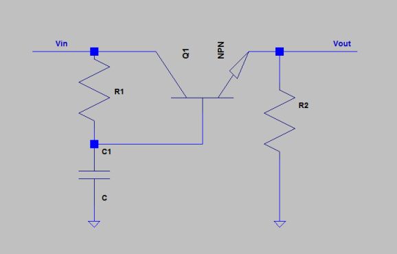
The following schematic represents the transistor based capacitance multiplier topology:
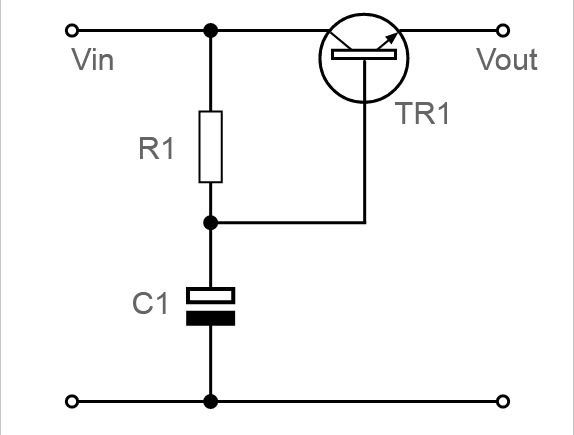
It is nothing else than an RC filter driving the base of a transistor follower. In this way, the emitter output voltage "follows" the filtered voltage one diode drop below, reducing the ripple of the input signal.
The input impedance of this circuit is roughly equal to the input impedance of the RC filter divided by the beta of the transistor, a factor between 20 and 1000 (or more). To obtain the same filtering result with a RC filter alone, one would have to use a much larger capacitance. For this reason, everything looks like the capacitance had been multiplied by beta, hence the name "capacitance multiplier".
An attractive feature of the capacitance multiplier is that it dissipates relatively few power with respect to the available current at the output. This is because the voltage drop across the transistor is often just what is needed to get rid of the ripple, but no more.
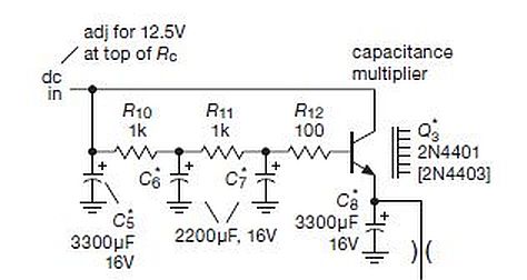
This circuit could also be seen as an activated RC filter; it is in fact the simplest possible active filter. Building upon this idea, nothing prevents exchanging the RC filter by a more efficient passive filter activated by a transistor, like in the following schematic extracted from a circuit in The Art of Electronics:
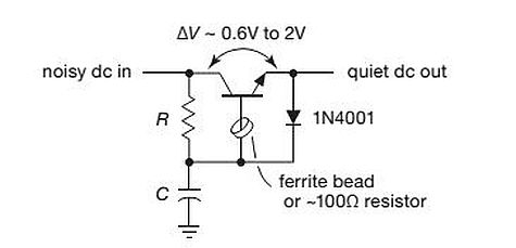
In the following schematic, a protection diode and a ferrite bead has been added to the basic topology. The ferrite bead is supposed to prevent fast oscillations occurring at the base of the transistor. This is often unnecessary for BJT transistors, but may be useful for FET transistors.
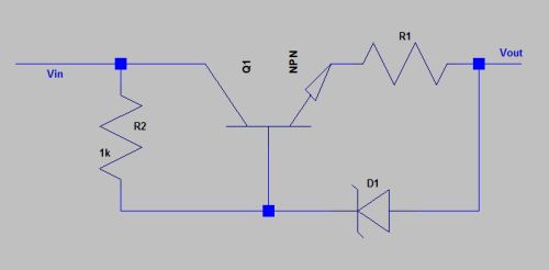
It is important to understand that the transistor cannot follow a voltage that is larger, or less than a diode drop below, the input voltage. So, it is often said that if the ripple is large, a resistor from the base of the transistor to ground may be introduced to increase the voltage drop, like in the following schematic:
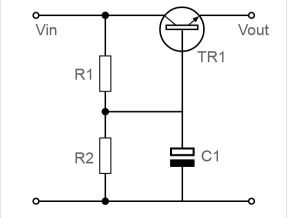
The choice of the resistor to ground R2 depends on design considerations regarding the maximum ripple, and the power dissipated by the transistor: there is a trade off between ripple reduction and power loss, as a greater voltage drop across the transistor increases the wasted power.
Another option is to use a FET transistor, whose threshold voltage (usually 2 to 5V) provides a larger room. In general, if power consumption is not an issue (e.g. for relatively low currents), a FET may be an excellent option because of its very high gate input impedance allowing a large R2 and/or a smaller C.
In the following schematic, a capacitance multiplier is shown "in context" inside the circuit of a AC to DC power supply:
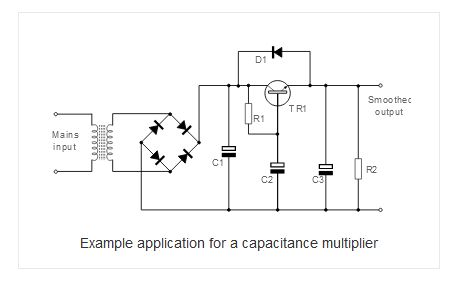
C1 is the storage capacitor after the rectifier bridge, and C3 is an additional capacitor to provide a faster answer to load variations.
There is also an op-amp capacitance multiplier version, but it is not dealt here for the following reasons:
- added complexity,
- can source only weak currents (unless unusual op-amps are used),
- falls into the realm of op-amp activated filters, where there are many other good options,
- most importantly, one of the main advantage of the transistor based topology is lost: indeed, the transistor topology is what could be called a "quasi-floating structure", meaning that it is connected to the ground by a capacitor only; this is not a problem in general, as capacitors rated for low to very high voltages exist and are inexpensive. In contrast, an op-amp has to be powered by some supply, which implies, almost always, a connection to Vcc and to the ground.
B. Problems and particular techniques
1. some design considerations:
-
The beta of the transistor has to be sufficiently large in order for the transistor to follow the base voltage; if the input impedance of the RC filter (that is, R) is too large with respect to beta, the base will not be able to drive the transistor at the desired current level. If this happens, a more muscular transistor is needed, often a Darlington, or a Sziklai pair. The Darlington provides two diodes voltage drop, increasing the ripple room but also the dissipated power, while the Sziklai pair makes the voltage drop by only one diode, decreasing both the ripple room and the dissipated power. In practice, a TIP122, or even the muscular TIP135 is just fine.
-
After choosing resistor R and beta as explained above, capacitor C should be chosen large enough in order for the base signal to be sufficiently quiet and not be spoiled by the base current (1/beta of the maximal current through the transistor).
-
The two points above are not an issue in general, if a FET transistor is used, because of its very high gate impedance. Nevertheless, a FET introduces a larger voltage drop (this could be an advantage according to the circumstances), and hence dissipates more power (always an inconvenient). In addition, the voltage drop is less controllable
-
For currents bigger than 0.3A (say), the power dissipated by the transistor has to be taken into account and a heat sink has to be added to the transistor.
2. Cascading capacitance multipliers
As explained in the previous sections, whenever the ripple is large, measures has to be taken to make the capacitance multiplier work well. As seen above, it is possible to consider using a FET, or to insert a resistor to ground. But here is another option sticking with the genuine topology, that works well most of the time and avoid design considerations: simply cascade two capacitance multipliers.
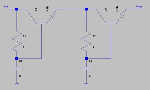
In this configuration, the first capacitance multiplier absorbs most of the ripple and dissipates most of the power. Then the second capacitance multiplier kills the remaining noise and needs only a modest heat sink, if any. The attenuation of the ripple follows the well known law for filter cascading: the resulting attenuation, in decibel, is the sum of the attenuation of each filter (in decibel).
3. Slow turn on
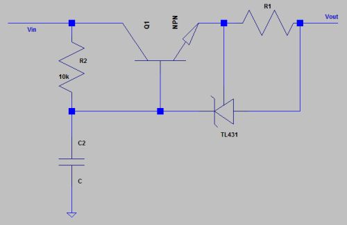
Perhaps somewhat unexpectedly, a capacitance multiplier can be used as a "slow turn on" circuit, in addition to its natural function: it suffices to set the RC time constant to the desired value (taking into account the base current). But we have now to make sure the capacitor discharges sufficiently quickly whenever the power is turned off, otherwise a near subsequent turn on of the circuit may result in a sharp voltage raising. This can be elegantly implemented with a BJT without spoiling the RC filter:
In the above schematic, R2 acts as a bleeder, and as a bonus, it makes the answer of the transistor more robust.
4. base/drain voltage rating problem and fast turn on
In the above section, the slow transistor turn on has been presented as a feature. But depending on the circumstances, it may be a nuisance, especially whenever a large R is needed.
Another more subtle and perverse problem of the capacitance multiplier is that when the power is turned on, the capacitor is discharged; so the base of the transistor is actually at ground, and the transistor is closed; now, if the the input voltage Vin is larger than the voltage rating of the transistor, it may burn; this contrasts with the small voltage drop across the transistor during the normal operation mode of the capacitance multiplier. The Art of Electronics warns about this issue and recommends a transistor with a voltage rating equal to Vin at least.
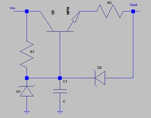
But here is a very simple trick that solves both problems at once and allows using modest transistors in most circumstances: It suffices to introduce a Zener diode (or better, a TVS diode) whose Zener voltage is a bit larger than the maximal possible voltage between the terminals of R (usually few volts), but lower by a diode drop at least than the maximal collector-emitter voltage transistor rating. This is illustrated in the following schematic:
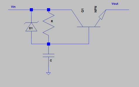
At turn on, the Zener/TVS opens extremely quickly and charges rapidly the capacitor. On the other hand, it ensures the collector-base voltage does not exceed the Zener voltage, hence also that the collector-emitter voltage does not exceed the Zener voltage + a diode drop. In this way, the transistor is protected.
The author has used this trick successfully in a 700V / 30mA adjustable voltage power supply he built, where the transistor in the capacitance multiplier was nothing else than the modest 2N3904!!! (I would recommend a more robust transistor though).
C. Circuit combining
It is difficult to resist to the temptation to expose how well a capacitor multiplier can combine with other, often desirable, features.
1. A digression toward voltage and current limiters
If you've ever tried to find "nominal" current limiter circuits, you probably know that they are not numerous. On the other hand, current source circuits abound everywhere. One day, the author realized what may be obvious for many electronic engineers, but is actually almost never told in books:
Most often, nothing distinguishes between a current source and a current limiter: a current source IS a current limiter.
The dual assertion for voltage is:
A voltage source IS (most often) a voltage limiter.
How does it work? it's simple: whenever the input current passing through a current source is lower than the current $I_{source}$ the source is supposed to deliver, this later does its best to pass as much current as possible, that is, all the available current. But whenever the available current is larger, the source limits it to $I_{source}$, that is, it acts as current limiter.
The dual assertion for voltage limiters can be explained in a similar way.
Now, the simplest possible activated current source, and hence, also, current limiter, is the following circuit:
The current limit value is set with $$I_{limit} = (V_{Zener} - 0.7)/R_1$$ for BJTs, and with $$I_{limit} = (V_{Zener} - V{thr})/R_1$$ for mosfets.
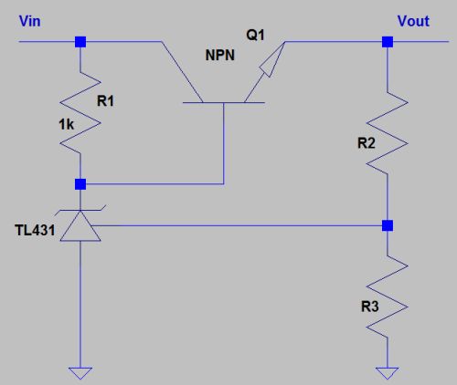
Notice that this is a floating circuit, an advantage. It is possible to improve both the precision and the low voltage range of this current limiter by using the TL431 voltage reference:
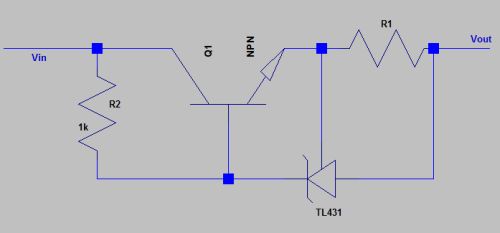
Here $I_{limit} = V_{ref}/R_1 = 2.5/R_1$.
Notice that the TL431 needs at least a cathode current of 1 mA to regulate; if Vd denotes the smallest voltage drop the whole circuit should be able to fit (necessarily, Vd > Vref), this imposes the limit $ (V_d - V_{ref})/R_2 > 1\ \rm mA$ in the above schematic, that is $R_2 < (V_d - V_{ref}) * 1000$. If R2 has to be larger, the NCP431 ultra low power programmable voltage reference, with its maximal 60 uA power supply, is an alternative(see Note 1 below for other options with regard to various design needs).
Also, when using these programmable voltage references with FET transistors, don't forget to protect them with a Zener diode whose voltage is below their maximal anode to cathode voltage rating, but above Vref: this is necessary because FETs do not possess the base-emitter diode of BJTs.
For mosfets, it may be advantageous to use a circuit not depending upon the threshold voltage; unfortunately, as was just explained, if R2 has to be large in the above circuit, the TL431 cannot regulate any more. Here is another solution where the current limit is set at 20 mA for an input voltage of 1000V, with a large resistor from Vcc to the gate of the mosfet:
This current limiter may be less precise and stable over the temperature range than the voltage reference based limiters, but it is nevertheless robust.
Now, regarding voltage limiting, the simplest activated voltage limiter circuit is probably the following:
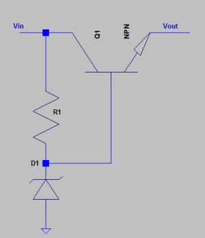
where the voltage limit is $V_{limit} = V_{Zener} - \text{1 diode drop}$. A TL431 version of this circuit is possible and obtains easily:
In the above circuit, the voltage limit is $V_{limit} = (1 + R_2/R_3)V_{ref} = 2.5(1+R_2/R_3)$.
Of course, in all the circuits of this section, one has to worry about considerations like transistor and resistor voltages rating, dissipated power etc.
2. Circuit combining
This part is just the conclusion of the previous section: one can combine together a capacitance multiplier with a current limiter and/or with a voltage limiter.
Here is a combination "capacitance multiplier" + "TL431 current limiter":
And here is an "all in one" combination "capacitance multiplier + current limiter + voltage limiter":
A final note: in these combinations, the trick in sec. B.4 is no more relevant: the transistor must to be able to sustain the maximal voltage Vin.
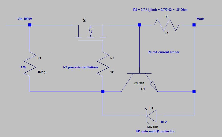
3. A design example
To build a pre-filtering stage for a power supply of Vin = 1000 V, with a ripple of 5V, 100Hz. The supply is able to deliver 25W. The current should be limited to some value.
-
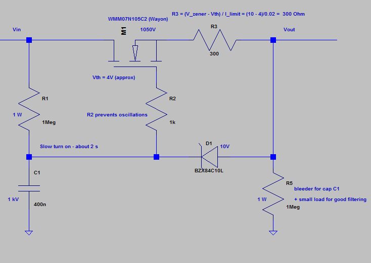
Decide what to use: a BJT or a mosfet. The choice here is relatively obvious, at high voltage, a mosfet is more robust. Furthermore, the relatively high voltage ripple just fits the V_thr of the mosfet. Most importantly, we need a very large resistor for the capacitance multiplier because it is also used by the current limiter, so, only the high input impedance of a mosfet is suitable. Here the mosfet has to sustain a voltage of 1000V or so. So, we choose a 1050V mosfet, like the Wayon WMM07N105C2.
-
Next, fix the current limit: the maximal available power to the load is $V_{in} I_{limit}$, hence we should have $V_{in}I_{limit} \leq 20 W $ (to be conservative). We choose $I_{limit} = 20/V_{in} = 20\ mA$. Notice also that this value, 20 W, is the maximal power the transistor may dissipate in "current limiter mode". So, just check the transistor can handle 20W in its operating region. Otherwise, choose a suitable transistor.
-
Heat sink for the transistor: 25 W (say)
-
Choose the value of the Zener in the current limiter: 10V seems fine as it allows the mosfet to fully turn on.
-
Now, the value of the resistor in the current limiter in the previous section is given by $R = (10 -V_{thr})/0.02 = 300\ \Omega$.
-
Choose the resistor in the capacitance multiplier: since the resistor is also used for the current source, it should be able to sustain the whole voltage in case of short. A 1 Mega ohm resistor rated for 1W and 1000V seems fine. This makes the capacitance multiplier "slow turn on", but it is always a good idea to slowly turn on the power at high voltage: this prevents unexpected failures and ESD events, both in the supply and for the end user. So, let us accept happily the inevitable "slow turn on" here as an additional feature.
-
Choose the capacitor value in the capacitance multiplier. We want the supply to turn on in about 2 seconds, which is determined by the RC time constant. More precisely, we should have 2 = 5RC, or C = 400 nF.
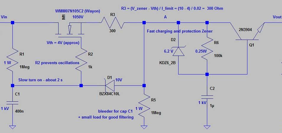
All the ingredients are ready; here is the schematic:
A simulation with no load (the worse case) gives a ripple of 0.5V at the output of this circuit (much less with a decent load):
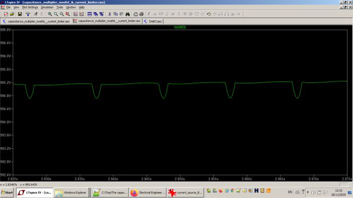
So, let add another capacitance multiplier stage, but using the trick in Sec. B. 4.:
Here is a simulation in the AC domain of the above circuit (see Appendix for a schematic of the whole simulation circuit), with a load of 100k:
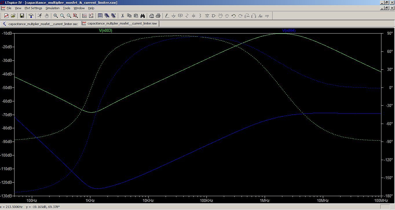
The green line is the noise attenuation at point A (the output of the first capacitance multiplier stage), and the blue line is the noise attenuation at V_out (the dashed lines are the phase plot and are irrelevant). Similar results obtains with loads of 10k, 100k, 1Meg etc: the final attenuation is always above 50 db, a huge smoothing factor.
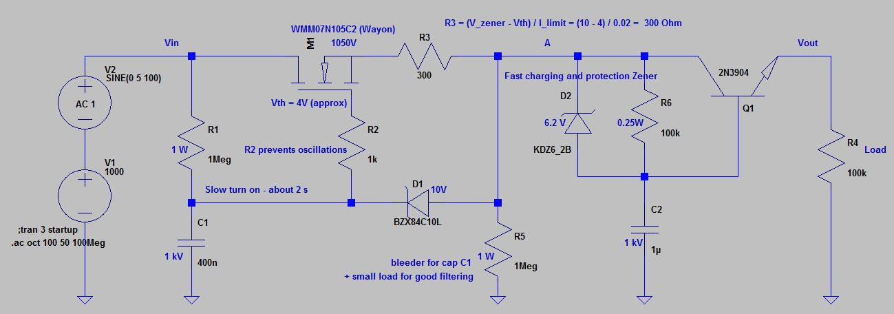
D. Appendix
The following complete circuit has been used for the last simulation in Sec. C. 3. :
E. Notes
Note 1: The TL431 and NPC431 have a reference voltage of about 2.5V, while the TLV431 has a reference voltage of about 1.2 V. Both the NPC431 and TLV431 need a very low power supply of 60-100 uA.
At the extreme, INTERSIL produces a variety of voltage references based on the FGA floating gate analog mosfet technology (like the ISL60002 series). They feature ultra-low supply current (e.g. 400nA), very high accuracy and ultra low tempco.
In general, the larger the reference voltage, the larger resistor R2 could be chosen in the schematic, an advantage for high voltage, where the usually low sourced current is not an issue for resistor R1. On the other hand, for sourcing stronger currents, a low reference voltage is an advantage, since it reduces the power dissipated by R1 in the schematic.
Finally, there also exist programmable references usable for reverse polarity sourcing: the LM4041 is an example, where the reference voltage is not relative to the ground but to the + supply.
Acknoledgments to Pete W for his comments about a part of the material in this note.

1 comment thread