Comments on What is the difference between emitter and collector of a transistor?
Parent
What is the difference between emitter and collector of a transistor?
In all descriptions of how (non-FET) transistors work I've seen, there is an inherent symmetry: There's either an n-doped layer between two p-doped, or a p-doped between two n-doped, and the description does not make any distinction between the two outer layers.
On the other hand, one of the connections to the outer layers is called emitter and the other collector. Also, in the transistor symbol in circuits, the difference is clearly marked by an arrow. Therefore I assume there actually is a difference.
Therefore I wonder: What is the difference between emitter and collector? What would happen if you would insert a transistor reversed?
Note: I'm physicist (so I can understand advanced descriptions on the physics level), but I don't have any experience with electronics.
Post
A bipolar junction transistor can be used as an amplifier, in which case some parameters of interest are $\alpha$ (the common-base current gain, equal to $I_C/I_E$) and $\beta$ (the common-emitter current gain, equal to $I_C/I_B$). (Here, $I_C$, $I_B$, and $I_E$ are the currents at the collector, base, and emitter, respectively.) It is usually desired that $\alpha$ and $\beta$ be "large" (with $\alpha$ almost equal to, but a little less than, 1, and $\beta$ much larger than 1).
From Wikipedia,
Typically, the emitter region is heavily doped compared to the other two layers, and the collector is doped more lightly than the base (collector doping is typically ten times lighter than base doping).
Also, for a planar BJT,
The collector surrounds the emitter region, making it almost impossible for the electrons injected into the base region to escape without being collected, thus making the resulting value of $\alpha$ very close to unity, and so, giving the transistor a large $\beta$. A cross-section view of a BJT indicates that the collector–base junction has a much larger area than the emitter–base junction.
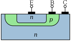
(Image of an NPN BJT taken from https://en.wikipedia.org/wiki/File:NPN_BJT_(Planar)_Cross-section.svg)
_Cross-section.svg)
The bipolar junction transistor, unlike other transistors, is usually not a symmetrical device. This means that interchanging the collector and the emitter makes the transistor leave the forward active mode and start to operate in reverse mode. Because the transistor's internal structure is usually optimized for forward-mode operation, interchanging the collector and the emitter makes the values of $\alpha$ and $\beta$ in reverse operation much smaller than those in forward operation; often the $\alpha$ of the reverse mode is lower than 0.5. The lack of symmetry is primarily due to the doping ratios of the emitter and the collector. The emitter is heavily doped, while the collector is lightly doped, allowing a large reverse bias voltage to be applied before the collector–base junction breaks down. The collector–base junction is reverse biased in normal operation. The reason the emitter is heavily doped is to increase the emitter injection efficiency: the ratio of carriers injected by the emitter to those injected by the base. For high current gain, most of the carriers injected into the emitter–base junction must come from the emitter.
1 comment thread

0 comment threads