What is the difference between emitter and collector of a transistor?
In all descriptions of how (non-FET) transistors work I've seen, there is an inherent symmetry: There's either an n-doped layer between two p-doped, or a p-doped between two n-doped, and the description does not make any distinction between the two outer layers.
On the other hand, one of the connections to the outer layers is called emitter and the other collector. Also, in the transistor symbol in circuits, the difference is clearly marked by an arrow. Therefore I assume there actually is a difference.
Therefore I wonder: What is the difference between emitter and collector? What would happen if you would insert a transistor reversed?
Note: I'm physicist (so I can understand advanced descriptions on the physics level), but I don't have any experience with electronics.
2 answers
You are accessing this answer with a direct link, so it's being shown above all other answers regardless of its score. You can return to the normal view.
A bipolar junction transistor can be used as an amplifier, in which case some parameters of interest are $\alpha$ (the common-base current gain, equal to $I_C/I_E$) and $\beta$ (the common-emitter current gain, equal to $I_C/I_B$). (Here, $I_C$, $I_B$, and $I_E$ are the currents at the collector, base, and emitter, respectively.) It is usually desired that $\alpha$ and $\beta$ be "large" (with $\alpha$ almost equal to, but a little less than, 1, and $\beta$ much larger than 1).
From Wikipedia,
Typically, the emitter region is heavily doped compared to the other two layers, and the collector is doped more lightly than the base (collector doping is typically ten times lighter than base doping).
Also, for a planar BJT,
The collector surrounds the emitter region, making it almost impossible for the electrons injected into the base region to escape without being collected, thus making the resulting value of $\alpha$ very close to unity, and so, giving the transistor a large $\beta$. A cross-section view of a BJT indicates that the collector–base junction has a much larger area than the emitter–base junction.
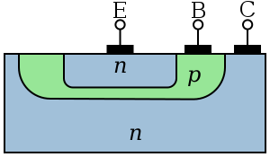
(Image of an NPN BJT taken from https://en.wikipedia.org/wiki/File:NPN_BJT_(Planar)_Cross-section.svg)
_Cross-section.svg)
The bipolar junction transistor, unlike other transistors, is usually not a symmetrical device. This means that interchanging the collector and the emitter makes the transistor leave the forward active mode and start to operate in reverse mode. Because the transistor's internal structure is usually optimized for forward-mode operation, interchanging the collector and the emitter makes the values of $\alpha$ and $\beta$ in reverse operation much smaller than those in forward operation; often the $\alpha$ of the reverse mode is lower than 0.5. The lack of symmetry is primarily due to the doping ratios of the emitter and the collector. The emitter is heavily doped, while the collector is lightly doped, allowing a large reverse bias voltage to be applied before the collector–base junction breaks down. The collector–base junction is reverse biased in normal operation. The reason the emitter is heavily doped is to increase the emitter injection efficiency: the ratio of carriers injected by the emitter to those injected by the base. For high current gain, most of the carriers injected into the emitter–base junction must come from the emitter.
1 comment thread
I see you already have an answer based on the device physics. I'll answer that this means in a circuit.
BJT (bipolar junction transistors) do work in reverse, at least somewhat. Generally, the characteristics aren't as good, particularly the gain. However, in most cases you still get some gain with the collector and emitter swapped.
I've actually had circuits where I accidentally installed a transistor backwards, and they worked. In that case, the circuit was tolerant of the lower gain. Circuits that require closer to the minimum guaranteed gain probably wouldn't work.
How a BJT works in reverse also depends on its geometry. Planar construction, like that shown by Joel Reyes Noche, doesn't work so well in reverse. That is because it is well optimized for charges in the base to make their way to the collector. Remember that the gain is the reciprocal of those that don't make it to the collector (go to the emitter instead). If you were to flip the collector and emitter, you can visualize how the system would be less efficient, meaning not quite such a large fraction of charges in the base would make it to the collector.
In a more simple NPN or PNP sandwich, reversing the transistor won't matter as much.
I naively assumed that all transistors of the same type have essentially identical characteristics; after all, unlike for other components, there seem to be no numbers written for them on circuit diagrams.
I'm not sure what you mean by "type". NPN versus PNP, or more specific, like 2N3906 versus 2N4401. In any case, there are many many individual models of transistors. These vary between each other in gain, maximum C-E voltage, maximum C current, highest usable frequency, power dissipation capability, pinout, package, and other parameters.
Any decent schematic absolutely will show the particular transistor model, or it will be accompanied by a BOM (bill of materials) that does. Such things must be specified to be able to build the unit.
Schematics that are only intended to conceptually show a circuit, like what may be posted here on this Q&A platform, might not always specify a particular model when that's not relevant to the concept. You can't build something like that, though, without somehow picking a model for each transistor.
1 comment thread


0 comment threads