Comments on Noise from oscillator on top layer to clock on bottom layer with VCC & GND layers between
Parent
Noise from oscillator on top layer to clock on bottom layer with VCC & GND layers between
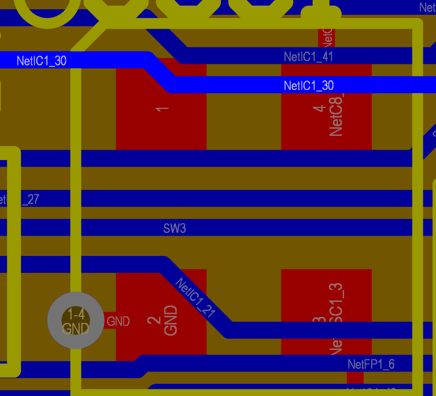
What effect does an oscillator potentially have on a SPI clk signal if the oscillator is on the top layer, with GND and VCC layer in between on a four layer board. I know running it on the same layer within a certain distance will have coupling effects that could cause noise and the 3W rule. I don't see people talking about different layers as much though. The clock is on the bottom like in the picture below. I know speed of oscillator and clock will likely determine if it will actually cause issues, but I am wondering about the general physics/practical noise that could be caused.
Post
It's hard to answer your specific case since you didn't label the layers in your picture, or which traces are doing what.
That said, a few traces crossing each other on different layers is not much coupling. In most cases of a typical board with a typical "SPI clock signal", there won't be any problem. The SPI clock signal is driven actively both directions by some CMOS output, probably with a few 100 Ω or less impedance. Even a few pF of capacitance to another signal shouldn't have much effect.
What effect does an oscillator potentially have on a SPI clk signal if the oscillator is on the top layer, with GND and VCC layer in between on a four layer board.
Essentially none if there is at least one complete ground or power plane between the two signals. Any plane with zero impedance relative to the signals, like a ground plane, will completely block capacitive effects.
There can still be small inductive effects, but those depend on current, not voltage, and require conductors running parallel to each other for some distance. Something like an SPI clock on a typical board should be basically unaffected.
Also keep in mind that with a 4 layer board and the two inner layers being used for ground and power planes, the signal are on the two outer layers. That puts them the full thickness of the board apart, usually about 62 mils (1.6 mm). Do the math to compute the capacitance at that separation for plausible areas, and you should see how minimal it is. And, that would only apply in places where there are no planes or traces in the inner layers.


0 comment threads