Meaning of some components around voltage reference in SMPS
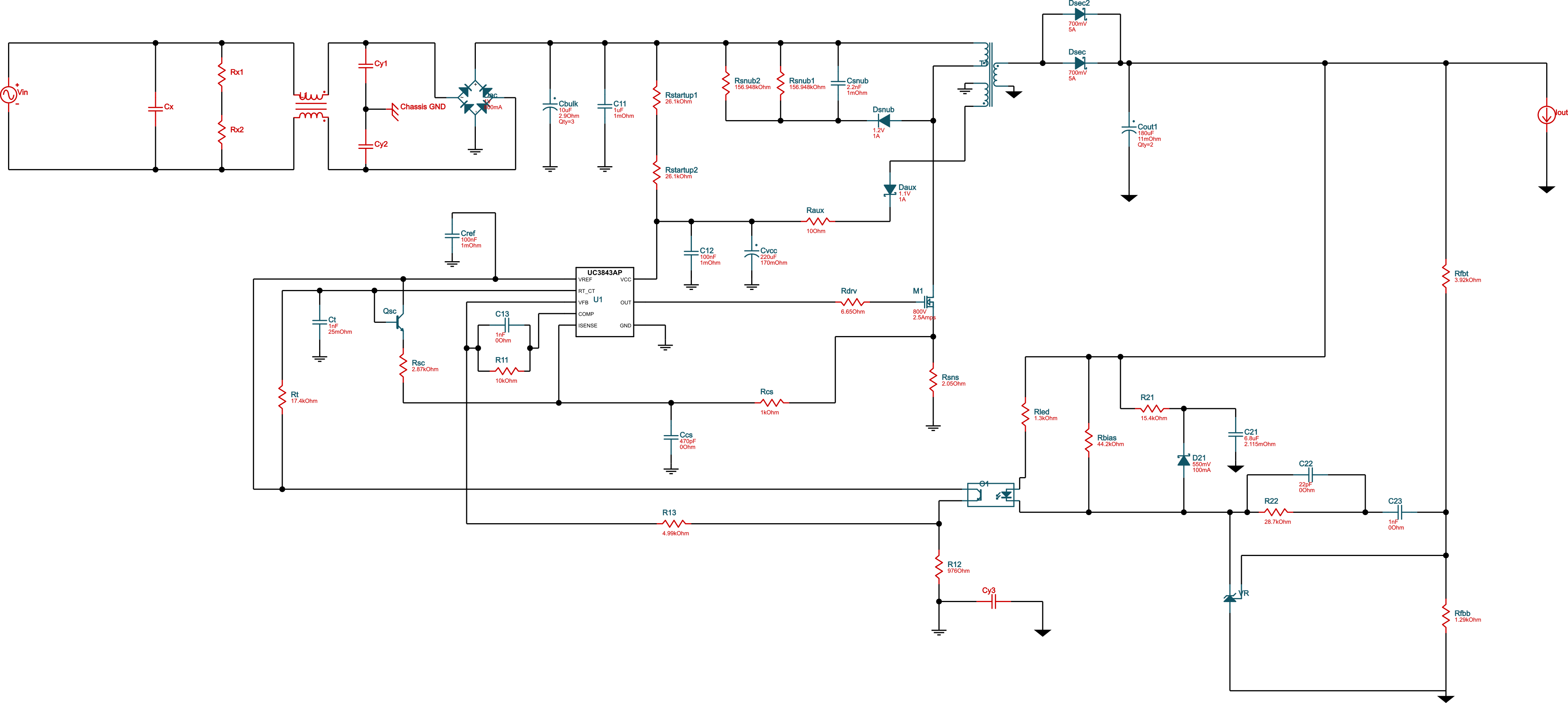
I have generated flyback convertor schematic by TI's Webench Power Designer.
Parameters:
- universal AC input (85-265V AC)
- 5V, 2A output
- isolated
- UC3843A controller
Basically I understand flyback topology, but I do not understand the function of some components around voltage reference (LMV431 used there).
What are R21, C21, D21 for? How to calculate values?
What are R22, C22, C23 for? How to calculate values?
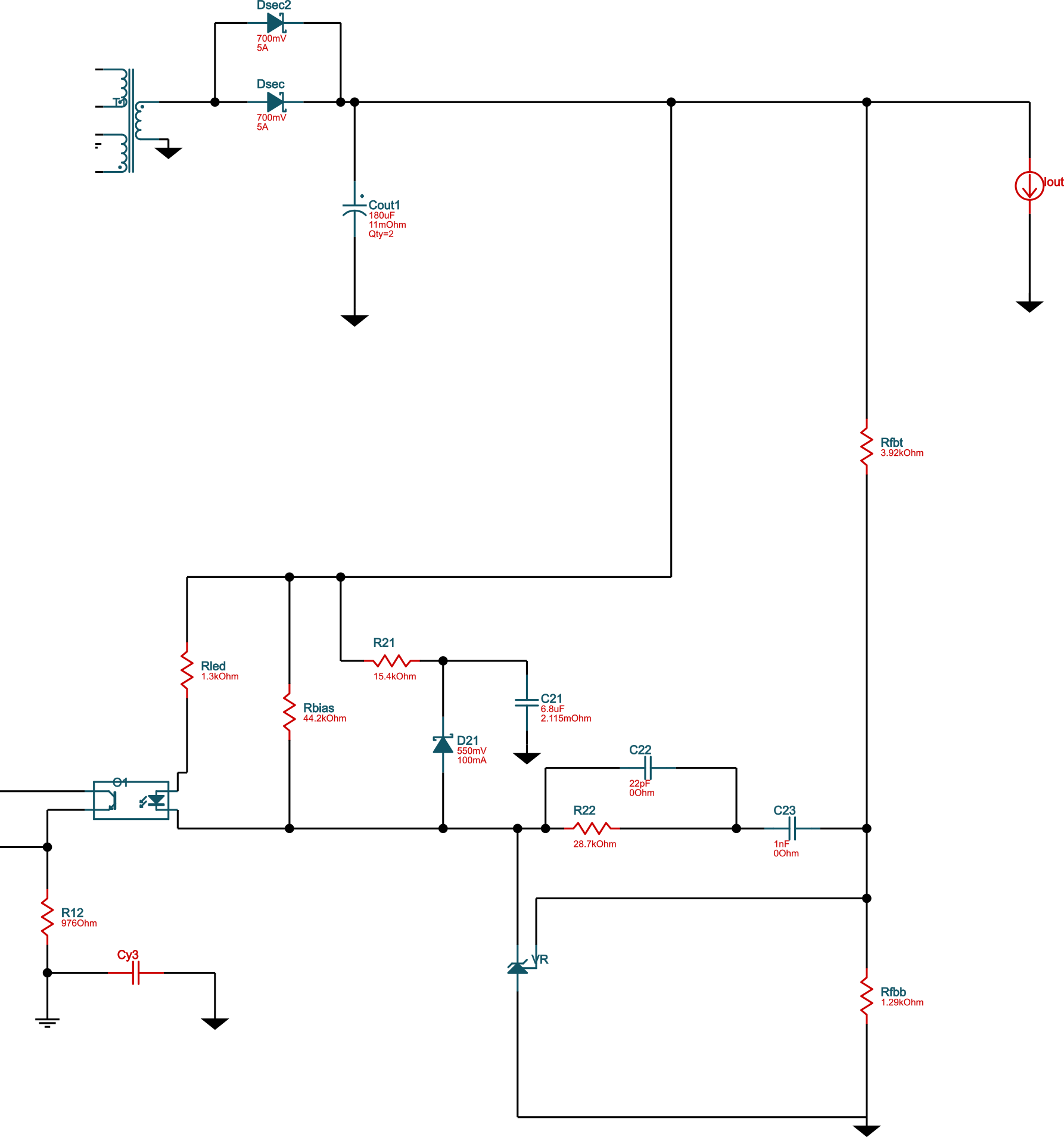
Just cut-out of the schematic:
Full schematic:
2 answers
R22, C22, C23, together with Rfbt (feedback top) and Rfbb (feedback bottom) form what is called a type II compensator, using TL431 as an opamp with built-in reference. The feedback network is a bit different than what you'd see -- usually it's R22 series with C23, and C22 in parallel with both of them, but it doesn't matter as long as the overall transfer function is achieved (there's probably a more readable way to write it):
$$H(s)=\dfrac{C_{22}||C_{23}}{R_{fbt}}\dfrac{s+\dfrac{1}{R_{22}(C_{22}+C_{23})}}{s(s+\dfrac{1}{R_{22}C_{22}})}$$
Its purpose is to add a pole and a zero in the feedback loop such that the phase gain at the cross-over is enough to avoid instabilities (usually around $60^\circ$ or so). If you'd use a SPICE simulation with a regular opamp (or ideal, in this case) and that particular network, you'd get this frequency response:
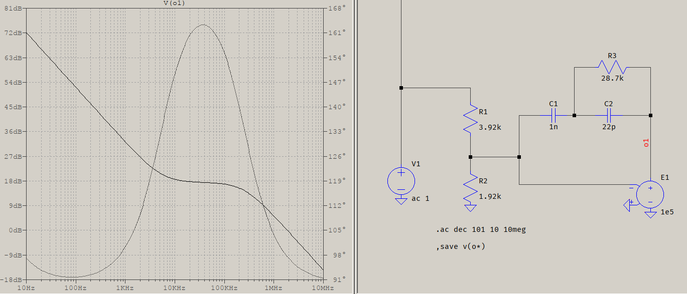
As you can see, there's a zero at around 10 kHz which adds phase (it goes positive), and a pole at 100+ kHz, whose purpose is to bring the phase back. The peak is about $70^\circ$ worth, and that's about how much phase would be gained if the peak coincided with the desired frequency (which I don't know, that's up to the designer).
About R/C/D21, I also have no clue about ther purpose. If the diode was meant for reverse voltage protection then why does it have R21 in there, and if it was meant as a sort of a voltage stabilizer, or limiter, then why did they use a Schottky and why isn't the voltage at the K junction used, instead? Olin's guess seems like a better one, about the pulse, but I give up.
Replying to your comment took too long, so I decided to edit the answer, instead.
The switching frequency of that flyback is 98kHz. So it corresponds with the chart of the compensator response you posted.
The switching frequency of the converter has nothing to do with the choice for the compensating pole. In fact, ...
Do I understand it correctly that it (R22, C22, C23) basically filters out 100kHz ripple from feedback?
... I never said anything about any ripple and filtering, but about stability and phase margin (gain).
I don't know how much you know these, so if I happen to repeat what you already know, just skip those lines. A flyback's "transformer" is nothing more than two (or more) coupled inductors. As such, there is a magnetizing inductance in there that, together with the output capacitor and the load, form an LC filter of varying quality factor (the load is not fixed). Because it's an LC filter it means that the phase shift at the output can reach $-180^\circ$ (asymptotically). Due to the presence of other parasitics and/or additional filtering (sometimes another small valued LC filter is added, for additional filtering), the phase may reach and exceed $-180^\circ$ when the magnitude gain is 0 dB, which can lead to oscillations. Even if it doesn't oscillate, operating the controller with a phase margin that is too close to the limit will cause the converter's transient response to wobble with a decaying exponential (best case scenario), eventually settling to a value (which is not at all desirable, but at least it settles down). The worst case is oscillation, but also wobbling uncontrollably, since the feedback loop will try to compensate the error and it ends up chasing its own tail. This is why, in practice, a phase margin of at least $40^\circ...50^\circ$ is used.
Therefore it's all about stability. If that pole would be needed at 1 MHz in order for the phase to be tamed, then that's where it would be placed. It's not the value of the frequency, but the value of the total phase which needs to be compensated due to the inherent filtering (and imperfections) that's part of a switching converter.
At first glance, R22, C22, and C23 look like a compensation network around the TL431. However, this doesn't make much sense because the TL431 is being run open loop. Rfbt and Rfbb divide down the output voltage. The TL431 is turned on when that reaches 2.5 V. The TL431 is therefore used to compare the output voltage to its regulation threshold. When the voltage is above the threshold, the TL431 turns on, which turns on the LED in the opto, which then signals the controller to stop making pulses.
A more likely reason for the R22,C22,C23 network is a little feed-forward. This would change the signal thru the opto from a simple high/low indication to have a small transition region. In that region, the opto will dither, somewhat proportional to the output voltage within that narrow detection region. This was probably used for a little less ripple on the output than would have resulted from a pure high/low indication.
As for R21,D21,C21, I have no idea unless the signal at the top of D21 goes somewhere else that is not show. Without that, all that this circuit appears to do is dump a pulse of current on the TL431 whenever it switches on. I can't come up with a reason why you would want to do that. In fact, that seems like a bad idea, so I don't know what the point is.


0 comment threads