Soft-start circuit behaviour
Let's take a soft-start circuit that looks like this:
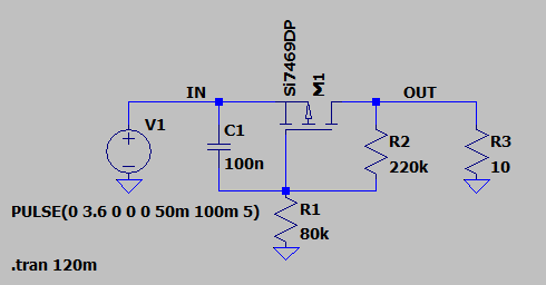
To my understanding, the function can be described as follows:
- C1 charges to open the gate. Value of C1 will dictate the soft-start delay.
- R2 and R1 form a divider that establishes a bias on the gate voltage once the FET opens.
- R1 also dictates startup time and serves to discharge C1 after input voltage is removed.
This circuit works in simulation and in the real world.
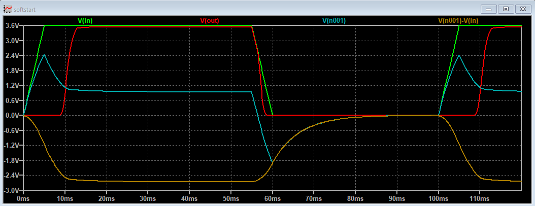
Here, $V_{in}$ in the input voltage, $V_{out}$ the output, and $V_{n001}$ in the gate voltage of the FET. $V_{n001}-V_{in}$ is then the gate-source voltage.
The capacitor starts charging and at a certain point a sufficient $V_{gs}$ is reached after which the FET will begin to open. This is clearly seen on the simulation. However, I am not certain why the R2/R1 divider is at all necessary since the soft-start fucntionality is achieved through the R1/C1 circuit.
Therefore the question: what is the point of using R2 in this circuit?
1 answer
First, let's redraw your schematic so that it's not so annoying to look at. High voltages go at top, low voltages at bottom, and logical flow left to right:
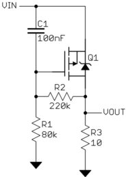
This is not a great soft-start circuit since it relies on unspecified behavior of the FET. It seems the strategy is to low pass filter the input power-on step to make a gradually decreasing gate voltage. That is then supposed to make the output voltage rise gradually.
The flaw with that logic is that there is no guarantee over what gate voltages the FET transitions from off to on. The datasheet may give a gate threshold voltage where the FET starts to turn on, but other than that the transfer function of gate voltage to channel current or resistance is unspecified.
You didn't say what range VIN is expected to be, but maybe R2 is to limit the gate voltage to what the FET can safely handle. If VIN can be 30 V, for example, and the maximum VGS of the FET is only 15 V, then just R1 to ground on the gate would cause excessive gate voltage. However, this is better addressed with a Zener diode between G and S.
R2 does provide a little negative feedback. The gate voltage decreases more rapidly (turns the FET on quicker) when VOUT is low. As VOUT rises, the gate gets lowered more gradually. This makes the slope of VOUT a little more consistent despite the unspecified gate to resistance relationship of the FET.
There are better ways, but also more complicated. Here is a snippet from a schematic of a real commercial product I designed:
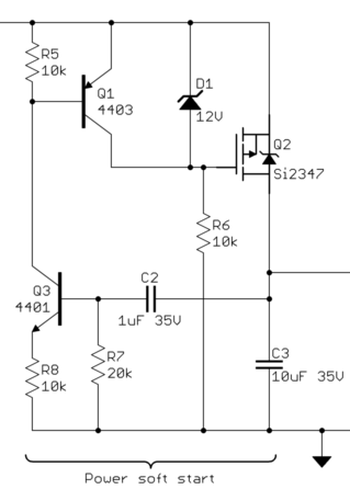
I have used this soft-start circuit a number of times. It's main purpose is to not glitch the 24 V power bus when this device is plugged in (hot-plugged). Nominal 24 V power comes in at top left, and internal power to the device is taken from the net at mid right (let's call that VOUT as in your circuit).
This circuit actively regulates the slope of VOUT. It does that without relying on a particular function of gate voltage to drain current or channel resistance of the FET.
Disregarding the circuitry to the left of D1, R6 pulls low on the gate of the FET, thereby turning it on when power is applied. D1 clamps the gate voltage to a safe level regardless of the input power voltage.
C2 and R7 are essentially a dV/dt detector. Note that a constant voltage is developed across R7 if the right end of C2 has a fixed voltage ramp on it. When this voltage across R7 gets large enough (dV/dt of VOUT gets high enough), then Q3 is turned on.
Turning on Q3 causes Q1 to turn on, which clamps the gate voltage to turn off FET Q2 a bit more. Eventually, R6 pulls the gate voltage low to fully turn on Q2. While Q2 is turning on, the additional circuitry slows down the turn-on of the FET to not exceed a particular slope of VOUT.
A few more details: R8 causes the impedance looking into the base of Q3 to be high relative to R7. That means the impedance on the left side of C2 is dominated by R7, keeping it relatively fixed and predictable. R5 makes sure Q1 doesn't come on due to a little leakage current or capacitively coupled noise. After startup, Q1 should be solidly off.
The slope control actually doesn't start from 0V, but starts at 2 diode drops. Is it wise to remove R8 and change value of R7 to 10k? So the startup time is the same, but it starts at 1 diode drop, instead of 2 diode drops.
Yes, the slope control doesn't start until VOUT reaches two diode drops above ground. In practice I found that not to be a problem. At that point, Q2 is just starting to turn on, with the gate voltage slope limited by R6 and the gate capacitance. This is not the point yet where small changes in gate voltage result in large changes in channel conduction.
No, R8 serves a purpose, as I described above. To reduce the slope control VOUT threshold, increase R5. R5 should probably be 100 kΩ. That reduces the voltage drop on R8 during active slope control to about 1/10 of a diode drop. One diode drop will always be there due to the B-E junction of Q3.
In what software did you draw these schematics?
I use Eagle for entering schematics and designing boards. To make schematic images for uploading here, the process is:
- Export the schematic to a TIF image file in monochrome at 600 DIP. Specifically, I use the command
export image filename monochrome 600;
I actually run my IMAGEBW ULP but all that does additional is to delete the target file if it exists before running the EXPORT command. Back when I created that ULP, the image write sometimes failed to correctly overwrite an existing file. That may be fixed by now.
- Shrink the raw schematic TIF file by a factor of 5 to a gray scale GIF. The result is now 120 DPI, but nicely anti-aliased. The same schematic exported directly from Eagle at 120 DPI would be pixelated. GIF is a good file format for gray scale since the result is efficiently but losslessly compressed.
I do this step by running my MAKE_SCHEM_GIF script. That runs my IMAGE_xxx image processing programs to do the work, then displays the final result in a small window. It always creates the final file \temp\b.gif, which is easy to enter when uploading here.
Here is the full IMAGEBW ULP:
#usage "<b><h1>Makes B+W image of current window contents.</h1></b>\n"
  "<p>"
  "The contents of the current editor window (intended for schematics) is "
  "written to the image file /temp/a.tif.  The image will be black and white "
  "written at 600 DPI.  This is suitable for then running the MAKE_SCHEM_GIF "
  "script afterwards."

string scr;                       //script to be executed when this ULP exits

//******************************************************************************
//
//   Executable code for main program.
//
  system (                        //make sure the temporary file doesn't exist
    "cmd /c if exist c:\\temp\\a.tif del c:\\temp\\a.tif");

  scr = filesetext (argv[0], ".scr"); //make script file of same generic name
  output (scr, "wtD") {           //open temporary script output file
    printf ("export image c:\\temp\\a.tif monochrome 600;\n");
    }                             //done writing the script

  exit ("script " + scr);         //exit ULP and run the script we just wrote
And here is the full MAKE_SCHEM_GIF script:
@echo off
rem
rem   MAKE_SCHEM_GIF
rem
rem   Creates a nicely filtered schematic GIF file from the raw Eagle output
rem   /temp/a.tif.  The resulting GIF file will be /temp/b.gif, and will be
rem   gray scale.
rem
setlocal
call treename_var /temp temp
cd /d "%temp%"
image_filter a b.img -shrink 5
image_copy b.img b.gif -form -gray
del b.img
image_info b.gif
server image_disp b.gif -dev medium
IMAGEBW and many other Eagle ULPs, scripts, libraries, and the like are included in my Eagle tools release. The IMAGE_xxx image processing programs and many other utilities are included in my Full runtime release. Both are available at: http://www.embedinc.com/pic/dload.htm.

1 comment thread