Post History
I've tryed to implement a local ground concept told by Olin Latrop here : He have told: (What I've perceived)You should not connect every gnd point instantly to gnd plane, since it can inject HF ...
#8: Question closed
by
 Olin Lathrop
·
2024-02-21T13:54:17Z (over 1 year ago)
Olin Lathrop
·
2024-02-21T13:54:17Z (over 1 year ago)
#7: Post edited
by
 mohammadsdtmnd
·
2024-02-20T18:02:15Z (over 1 year ago)
mohammadsdtmnd
·
2024-02-20T18:02:15Z (over 1 year ago)
- I've tryed to implement a local ground concept told by Olin Latrop [here ](https://electronics.stackexchange.com/a/15143/152533):
- He have told:
(What I've perceived)You should not connect every gnd point instantly to gnd plane, since it can inject HF signals created on gnd pin or decoupling pins directly through via to gnd plane, he suggested avoid it to avoid making that via an antenna which radiate energy into PCB substrate.- Case 1:
- -------------------------
- 
- Ic pins:
- 
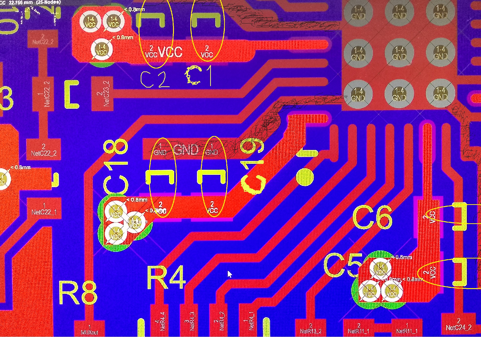
- Here C1 C2 C18 C19 C5 C6 are placed in path of Vcc and as Olin told the ground left unviad to prevent ground HF contamination.
- Schmatic:
- Vcc------------------Pin_Vcc
- | |
- ---C2 ---C1
- --- ---
- | |
- --- ---
- - -
- Like the above also for other C's.
- Case 2:
- --------------------------
- 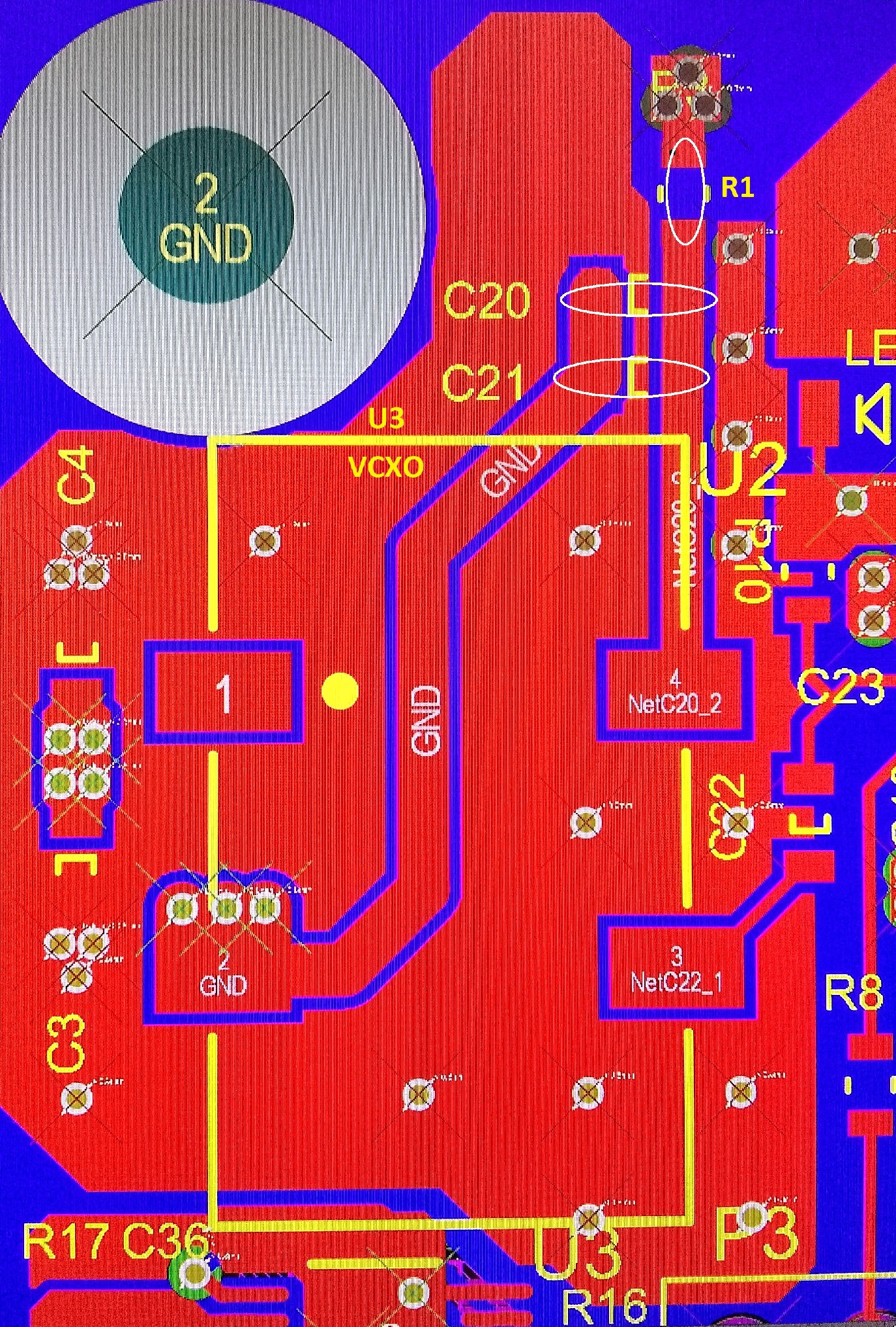
- Here you see R1 C20 C21 are placed in path of Vcc (injected with 3 via on top of picture) and ground left unviaad to prevent ground, the HF contamination.
- Vcc--~~~~------------------Pin_Vcc
- R1 | |
- ---C20 ---C21
- --- ---
- | |
- --- ---
- - -
- Not related note: The polygon pour is vcc to increase gnd vcc capacitance. I didn't connect that vcc to vcc polygon case my sensation told me to not connect them in layer 1(to layer). Originally the layer 3 is vcc.
- Am I right. And is this the best theory(Olin Latrop's theory)?
- I've tryed to implement a local ground concept told by Olin Latrop [here ](https://electronics.stackexchange.com/a/15143/152533):
- He have told:
- (What I've perceived)You should not connect every gnd point instantly to gnd plane, since it can inject HF signals created on gnd pin or decoupling pins directly through via to gnd plane, he suggested avoid it to not making that via an energy radiator into PCB substrate and prevent this diruption to couple into entire board elements.
- Case 1:
- -------------------------
- 
- Ic pins:
- 
- Here C1 C2 C18 C19 C5 C6 are placed in path of Vcc and as Olin told the ground left unviad to prevent ground HF contamination.
- Schmatic:
- Vcc------------------Pin_Vcc
- | |
- ---C2 ---C1
- --- ---
- | |
- --- ---
- - -
- Like the above also for other C's.
- Case 2:
- --------------------------
- 
- Here you see R1 C20 C21 are placed in path of Vcc (injected with 3 via on top of picture) and ground left unviaad to prevent ground, the HF contamination.
- Vcc--~~~~------------------Pin_Vcc
- R1 | |
- ---C20 ---C21
- --- ---
- | |
- --- ---
- - -
- Not related note: The polygon pour is vcc to increase gnd vcc capacitance. I didn't connect that vcc to vcc polygon case my sensation told me to not connect them in layer 1(to layer). Originally the layer 3 is vcc.
- Am I right. And is this the best theory(Olin Latrop's theory)?
#6: Post edited
by
mohammadsdtmnd
·
2024-02-20T17:53:32Z (over 1 year ago)
- I've tryed to implement a local ground concept told by Olin Latrop [here ](https://electronics.stackexchange.com/a/15143/152533):
- He have told:
- (What I've perceived)You should not connect every gnd point instantly to gnd plane, since it can inject HF signals created on gnd pin or decoupling pins directly through via to gnd plane, he suggested avoid it to avoid making that via an antenna which radiate energy into PCB substrate.
- Case 1:
- -------------------------
- 
- Ic pins:
- 
- Here C1 C2 C18 C19 C5 C6 are placed in path of Vcc and as Olin told the ground left unviad to prevent ground HF contamination.
- Schmatic:
- Vcc------------------Pin_Vcc
- | |
- ---C2 ---C1
- --- ---
- | |
- --- ---
- - -
- Like the above also for other C's.
- Case 2:
- --------------------------
- 
- Here you see R1 C20 C21 are placed in path of Vcc (injected with 3 via on top of picture) and ground left unviaad to prevent ground, the HF contamination.
- Vcc--~~~~------------------Pin_Vcc
- R1 | |
- ---C20 ---C21
- --- ---
- | |
- --- ---
- - -
Not related note: The polygon pour is vcc to increase gnd vcc capacitance. I didn't connect that vcc to vcc case my sensation told me to not connect them in layer 1(to layer). Originally the layer 3 is vcc.- Am I right. And is this the best theory(Olin Latrop's theory)?
- I've tryed to implement a local ground concept told by Olin Latrop [here ](https://electronics.stackexchange.com/a/15143/152533):
- He have told:
- (What I've perceived)You should not connect every gnd point instantly to gnd plane, since it can inject HF signals created on gnd pin or decoupling pins directly through via to gnd plane, he suggested avoid it to avoid making that via an antenna which radiate energy into PCB substrate.
- Case 1:
- -------------------------
- 
- Ic pins:
- 
- Here C1 C2 C18 C19 C5 C6 are placed in path of Vcc and as Olin told the ground left unviad to prevent ground HF contamination.
- Schmatic:
- Vcc------------------Pin_Vcc
- | |
- ---C2 ---C1
- --- ---
- | |
- --- ---
- - -
- Like the above also for other C's.
- Case 2:
- --------------------------
- 
- Here you see R1 C20 C21 are placed in path of Vcc (injected with 3 via on top of picture) and ground left unviaad to prevent ground, the HF contamination.
- Vcc--~~~~------------------Pin_Vcc
- R1 | |
- ---C20 ---C21
- --- ---
- | |
- --- ---
- - -
- Not related note: The polygon pour is vcc to increase gnd vcc capacitance. I didn't connect that vcc to vcc polygon case my sensation told me to not connect them in layer 1(to layer). Originally the layer 3 is vcc.
- Am I right. And is this the best theory(Olin Latrop's theory)?
#5: Post edited
by
mohammadsdtmnd
·
2024-02-20T17:50:36Z (over 1 year ago)
more schmatic clarification
- I've tryed to implement a local ground concept told by Olin Latrop [here ](https://electronics.stackexchange.com/a/15143/152533):
- He have told:
- (What I've perceived)You should not connect every gnd point instantly to gnd plane, since it can inject HF signals created on gnd pin or decoupling pins directly through via to gnd plane, he suggested avoid it to avoid making that via an antenna which radiate energy into PCB substrate.
- Case 1:
- -------------------------
- 
- Here C1 C2 C18 C19 C5 C6 are placed in path of Vcc and as Olin told the ground left unviad to prevent ground HF contamination.
- Schmatic:
- Vcc------------------Pin_Vcc
- | |
- ---C2 ---C1
- --- ---
- | |
- --- ---
- - -
- Like the above also for other C's.
- Case 2:
- --------------------------
- 
- Here you see R1 C20 C21 are placed in path of Vcc (injected with 3 via on top of picture) and ground left unviaad to prevent ground, the HF contamination.
- Vcc--~~~~------------------Pin_Vcc
- R1 | |
- ---C20 ---C21
- --- ---
- | |
- --- ---
- - -
- Not related note: The polygon pour is vcc to increase gnd vcc capacitance. I didn't connect that vcc to vcc case my sensation told me to not connect them in layer 1(to layer). Originally the layer 3 is vcc.
Am I right. Is this the best theory(Olin Latrop's theory)?
- I've tryed to implement a local ground concept told by Olin Latrop [here ](https://electronics.stackexchange.com/a/15143/152533):
- He have told:
- (What I've perceived)You should not connect every gnd point instantly to gnd plane, since it can inject HF signals created on gnd pin or decoupling pins directly through via to gnd plane, he suggested avoid it to avoid making that via an antenna which radiate energy into PCB substrate.
- Case 1:
- -------------------------
- 
- Ic pins:
- 
- Here C1 C2 C18 C19 C5 C6 are placed in path of Vcc and as Olin told the ground left unviad to prevent ground HF contamination.
- Schmatic:
- Vcc------------------Pin_Vcc
- | |
- ---C2 ---C1
- --- ---
- | |
- --- ---
- - -
- Like the above also for other C's.
- Case 2:
- --------------------------
- 
- Here you see R1 C20 C21 are placed in path of Vcc (injected with 3 via on top of picture) and ground left unviaad to prevent ground, the HF contamination.
- Vcc--~~~~------------------Pin_Vcc
- R1 | |
- ---C20 ---C21
- --- ---
- | |
- --- ---
- - -
- Not related note: The polygon pour is vcc to increase gnd vcc capacitance. I didn't connect that vcc to vcc case my sensation told me to not connect them in layer 1(to layer). Originally the layer 3 is vcc.
- Am I right. And is this the best theory(Olin Latrop's theory)?
#4: Post edited
by
mohammadsdtmnd
·
2024-02-18T18:47:53Z (over 1 year ago)
- I've tryed to implement a local ground concept told by Olin Latrop [here ](https://electronics.stackexchange.com/a/15143/152533):
- He have told:
- (What I've perceived)You should not connect every gnd point instantly to gnd plane, since it can inject HF signals created on gnd pin or decoupling pins directly through via to gnd plane, he suggested avoid it to avoid making that via an antenna which radiate energy into PCB substrate.
- Case 1:
- -------------------------
- 
- Here C1 C2 C18 C19 C5 C6 are placed in path of Vcc and as Olin told the ground left unviad to prevent ground HF contamination.
- Schmatic:
- Vcc------------------Pin_Vcc
- | |
- ---C2 ---C1
- --- ---
- | |
- --- ---
- - -
Like the above also for other C.- Case 2:
- --------------------------
- 
Here you see R1 C20 C21 are placed in path of Vcc (injected with 3 via on top of picture) and ground left unviaad to prevent ground, the HF contamination. Not related note: The polygon pour is vcc to increase gnd vcc capacitance. I didn't connect that vcc to vcc case my sensation told me to not connect them in layer 1(to layer). Originally the layer 3 is vcc.- Am I right. Is this the best theory(Olin Latrop's theory)?
- I've tryed to implement a local ground concept told by Olin Latrop [here ](https://electronics.stackexchange.com/a/15143/152533):
- He have told:
- (What I've perceived)You should not connect every gnd point instantly to gnd plane, since it can inject HF signals created on gnd pin or decoupling pins directly through via to gnd plane, he suggested avoid it to avoid making that via an antenna which radiate energy into PCB substrate.
- Case 1:
- -------------------------
- 
- Here C1 C2 C18 C19 C5 C6 are placed in path of Vcc and as Olin told the ground left unviad to prevent ground HF contamination.
- Schmatic:
- Vcc------------------Pin_Vcc
- | |
- ---C2 ---C1
- --- ---
- | |
- --- ---
- - -
- Like the above also for other C's.
- Case 2:
- --------------------------
- 
- Here you see R1 C20 C21 are placed in path of Vcc (injected with 3 via on top of picture) and ground left unviaad to prevent ground, the HF contamination.
- Vcc--~~~~------------------Pin_Vcc
- R1 | |
- ---C20 ---C21
- --- ---
- | |
- --- ---
- - -
- Not related note: The polygon pour is vcc to increase gnd vcc capacitance. I didn't connect that vcc to vcc case my sensation told me to not connect them in layer 1(to layer). Originally the layer 3 is vcc.
- Am I right. Is this the best theory(Olin Latrop's theory)?
#3: Post edited
by
mohammadsdtmnd
·
2024-02-18T18:43:38Z (over 1 year ago)
I've tryed to implement a local ground concept told by Olin Latrop [here ](https://electronics.stackexchange.com/a/15143/152533).- Case 1:
- -------------------------
- 
- Here C1 C2 C18 C19 C5 C6 are placed in path of Vcc and as Olin told the ground left unviad to prevent ground HF contamination.
- Case 2:
- --------------------------
- 
Here you see R1 C20 C21 are placed in path of Vcc and ground left unviaad to prevent ground, the HF contamination. Not related note: The polygon pour is vcc to increase gnd vcc capacitance. I didn't connect that vcc to vcc case my sensation told me to not connect them in layer 1(to layer). Originally the layer 3 is vcc.- Am I right. Is this the best theory(Olin Latrop's theory)?
- I've tryed to implement a local ground concept told by Olin Latrop [here ](https://electronics.stackexchange.com/a/15143/152533):
- He have told:
- (What I've perceived)You should not connect every gnd point instantly to gnd plane, since it can inject HF signals created on gnd pin or decoupling pins directly through via to gnd plane, he suggested avoid it to avoid making that via an antenna which radiate energy into PCB substrate.
- Case 1:
- -------------------------
- 
- Here C1 C2 C18 C19 C5 C6 are placed in path of Vcc and as Olin told the ground left unviad to prevent ground HF contamination.
- Schmatic:
- Vcc------------------Pin_Vcc
- | |
- ---C2 ---C1
- --- ---
- | |
- --- ---
- - -
- Like the above also for other C.
- Case 2:
- --------------------------
- 
- Here you see R1 C20 C21 are placed in path of Vcc (injected with 3 via on top of picture) and ground left unviaad to prevent ground, the HF contamination. Not related note: The polygon pour is vcc to increase gnd vcc capacitance. I didn't connect that vcc to vcc case my sensation told me to not connect them in layer 1(to layer). Originally the layer 3 is vcc.
- Am I right. Is this the best theory(Olin Latrop's theory)?
#2: Post edited
by
mohammadsdtmnd
·
2024-02-18T15:33:02Z (over 1 year ago)
- I've tryed to implement a local ground concept told by Olin Latrop [here ](https://electronics.stackexchange.com/a/15143/152533).
- Case 1:
- -------------------------
- 
- Here C1 C2 C18 C19 C5 C6 are placed in path of Vcc and as Olin told the ground left unviad to prevent ground HF contamination.
- Case 2:
- --------------------------
- 
Here you see R1 C20 C21 are placed in path of Vcc and ground left unviaad to prevent ground, the HF contamination.- Am I right. Is this the best theory(Olin Latrop's theory)?
- I've tryed to implement a local ground concept told by Olin Latrop [here ](https://electronics.stackexchange.com/a/15143/152533).
- Case 1:
- -------------------------
- 
- Here C1 C2 C18 C19 C5 C6 are placed in path of Vcc and as Olin told the ground left unviad to prevent ground HF contamination.
- Case 2:
- --------------------------
- 
- Here you see R1 C20 C21 are placed in path of Vcc and ground left unviaad to prevent ground, the HF contamination. Not related note: The polygon pour is vcc to increase gnd vcc capacitance. I didn't connect that vcc to vcc case my sensation told me to not connect them in layer 1(to layer). Originally the layer 3 is vcc.
- Am I right. Is this the best theory(Olin Latrop's theory)?
#1: Initial revision
by
mohammadsdtmnd
·
2024-02-18T15:28:39Z (over 1 year ago)
Implementing local ground theory on PCB power distribution
I've tryed to implement a local ground concept told by Olin Latrop [here ](https://electronics.stackexchange.com/a/15143/152533). Case 1: -------------------------  Here C1 C2 C18 C19 C5 C6 are placed in path of Vcc and as Olin told the ground left unviad to prevent ground HF contamination. Case 2: --------------------------  Here you see R1 C20 C21 are placed in path of Vcc and ground left unviaad to prevent ground, the HF contamination. Am I right. Is this the best theory(Olin Latrop's theory)?