Communities

Writing
Writing
Codidact Meta
Codidact Meta
The Great Outdoors
The Great Outdoors
Photography & Video
Photography & Video
Scientific Speculation
Cooking
Cooking
Electrical Engineering
Judaism
Judaism
Languages & Linguistics
Software Development
Mathematics
Mathematics
Christianity
Christianity
Code Golf
Code Golf
Music
Music
Physics
Physics
Linux Systems
Linux Systems
Power Users
Power Users
Tabletop RPGs
Tabletop RPGs
Community Proposals
Community Proposals
tag:snake search within a tag
answers:0 unanswered questions
user:xxxx search by author id
score:0.5 posts with 0.5+ score
"snake oil" exact phrase
votes:4 posts with 4+ votes
created:<1w created < 1 week ago
post_type:xxxx type of post
Search help
Notifications
Mark all as read See all your notifications »
Q&A

Comments on ESD Protection - Differential Amplifier

Parent

ESD Protection - Differential Amplifier

+2
−1

Circuit under discussion


More about the circuit

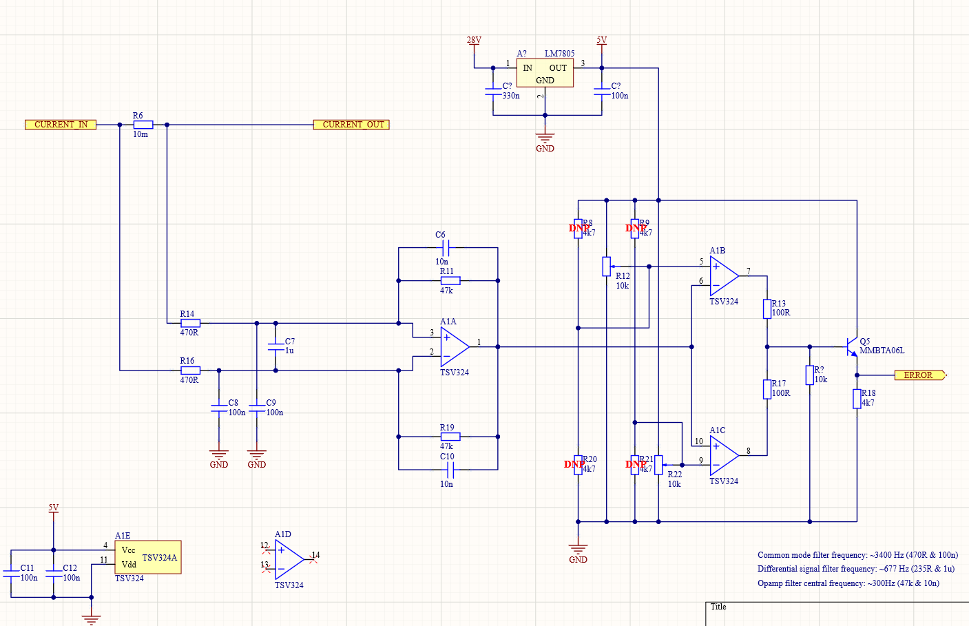
The circuit is sensing (low side sensing for many reasons) current used to power up the lights with 28V(part of the schematics not shown here -> relay with LC filter on the output side to limit the inrush current). The nominal current flowing through R6 is around 0.2A but could be up to 1.5A in peaks(peaks last around 100ms).

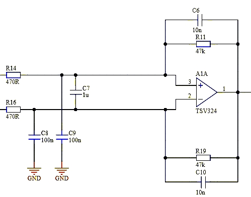
First opamp "A1A" is used to convert the differential signal seen on R6(around 200mV) to a single-ended signal with a ~300Hz.

R14, C9, R16, C8, and C7 are here for diff and common mode filtering(cut-off frequencies shown in the bottom right corner of the picture).

Using R12 and R22 around "A1B" and "A1C" I will trim the precise voltage values so that open circuit and overcurrent events flowing through R6 are detectable.

The information whether the circuit is open or there is overcurrent will be reported through Q5 to another device(not on this PCB - most likely industrial computer 5V Input).


Question

How would you position the TVS diodes around the "A1A" inputs so that circuit stays the same but become as immune to ESD events as possible?

ESD that we are talking about here is +-15kV with 330R and 150pF model(IEC6100-4-2 Class 4).


EDIT Per Andy Aka's suggestion, I am adding more details and maybe further explaining my question. Overall picture

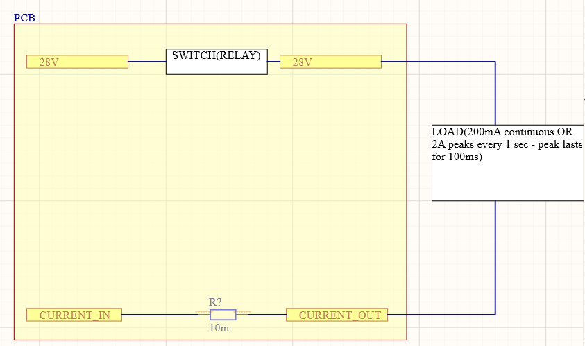
The load is floating while the bus voltage(28V on the picture) could be between 24V and 32V.

I am worried that +-15kV air discharge will kill "A1A" so I want to protect it with clever positioning of TVS Diodes across the opamp inputs.

Why do I think TVS diodes are needed?

If I would use this circuit as-is and expose it to ESD testing I would blow R14 and R16 because they are 125mW rated. Adding TVS in front of it would dump the usual ESD voltage to a level 200-500V where RC filter on the input could do the job easier.

Are TVS diodes needed in order to keep A1 opamp safe during Class 4 ESD strike? If they are not, how to place them?

History
Why does this post require moderator attention?
You might want to add some details to your flag.
Why should this post be closed?

1 comment thread

General comments (4 comments)
Post
+2
−0

Not a diff amp

Something doesn't make sense here. You want A1A to act as a differential amplifier, but that's not how you wired it:

Image

Here is a real diff amp:

Image

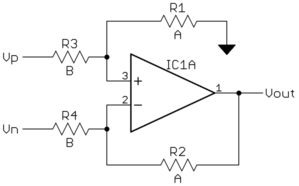
Note how the right side of R1 is tied to ground, not the opamp output.

The diff amp above is really a 3-input circuit. The output is the difference between the two inputs at left, multiplied by the gain (A/B in this example), then added to the reference input. In my circuit the reference input is the right side of R1, which is tied to ground in this example. Therefore, the amplified difference output will be relative to ground.

You have the reference input tied to the output. That makes the output indeterminate for ideal parts. All values of output satisfy the constraints when the inputs are equal.

One way to see this is to analyze your circuit with the left ends of R14 and R16 tied to ground. What will the output be? Whatever value you pick for the output, it will be divided by the same amount at each opamp input. No matter what the output voltage is, the opamp inputs will be the same.

TVSs

You don't need any TVSs.

The zap you specified (15 kV on 150 pF with 330 Ω in series) is going to disrupt the signal. Your only aim therefore is to protect the circuit from physical damage.

You already have 470 Ω followed by 100 nF to ground on each input. That should be enough to limit short zaps to the point where the protection circuitry in the opamp can handle the rest.

Your input capacitors are (100 nF)/(150 pF) = 667 times larger than the capacitance holding the static charge. That alone attenuates the 15 kV to 22.5 V. The input capacitors would only rise from 0 to 22.5 V with nothing else in the circuit.

The time constant of the rise would be (330 Ω + 470 Ω)(100 nF) = 80 µs. Or, we can look at this in frequency space as a single pole low pass filter at 2 kHz. Either way, it should be clear that any active ESD protection circuitry in the opamp can easily react in the time necessary to clamp the voltage.

I didn't look up your opamp since you didn't provide a datasheet link, so it's your job to check how its inputs are protected. But unless this device is unusual, there is no problem here to solve.

History
Why does this post require moderator attention?
You might want to add some details to your flag.

1 comment thread

General comments (14 comments)
General comments
Circuit fantasist‭ wrote over 3 years ago · edited over 3 years ago

You made me begin thinking about the "3-input diff amp"... It looks to me as a sort of a "summing-subtracting circuit". R3-R1 network is a passive voltage summer with weighted inputs. So Vp and Vref (0 V here since R1 is grounded) are summed according to the superposition principle - Vp.R1/(R1 + R3) + Vref.R3/(R1 + R3) and then multiplied by the ratio (R2 + R4)/R4 of the non-inverting amplifier. Vn is multiplied by the ratio -R2/R4 of the inverting amplifier. Both partial voltages are summed...

Circuit fantasist‭ wrote over 3 years ago

You have considered a very interesting situation in the OP's circuit when "left ends of R14 and R16 are tied to ground". Actually, this is a NIC. In this circuit, there are two kinds of feedback - negative (R16-R19) and positive (R14-R19). To be stable, this circuit requires the negative feedback to dominate over the positive one. But here they are equal... and this is not a stable state. I have considered it in this story: https://en.wikibooks.org/wiki/Circuit_Idea/Negative_Impedance_Converter.

2kind‭ wrote over 3 years ago

Thanks Olin! You are right, the A1A is not connected correctly.

https://www.st.com/resource/en/datasheet/tsv324a.pdf

The data about ESD is very vague - it says it could withstand 2kV using Human Body Model, but for example, doesn't have a schematic of how the opamp is realized internally like some manufacturers tend to.

I think 22V along with 80us tau is enough to keep it safe.

Circuit fantasist‭ wrote over 3 years ago · edited over 3 years ago

@2kind‭, Thanks to your mistake you "invented" an ingenious circuit-:) This is how great inventions are sometimes made!

Olin Lathrop‭ wrote over 3 years ago

@Circ: No, what he "invented" was just a comparator with a lot more parts than necessary.

Circuit fantasist‭ wrote over 3 years ago · edited over 3 years ago

Olin, I understand you since the final result is an op-amp without any feedback, i.e., a "comparator without hysteresis". But actually there are two feedbacks (negative and positive) that neutralize each other and the final result is "no feedback". But this state is unstable - it is enough for the positive feedback to slightly prevail over the negative one and the circuit will become a latch. That is why it is done so that the negative feedback dominates... and this is the circuit of NIC.

Olin Lathrop‭ wrote over 3 years ago

@Circ: No, a little positive feedback doesn't make it a latch. It adds hysteresis. The more positive feedback you add, the larger the hysteresis interval.

Circuit fantasist‭ wrote over 3 years ago · edited over 3 years ago

@Olin, first to move here my comment from below where I had put it wrong: If the four resistors were absolutely equal and the op-amp was ideal, the circuit would be identical as a bare op-amp without feedback (resistors). Now about your last comment above...

Circuit fantasist‭ wrote over 3 years ago

Every (op-amp) circuit with positive feedback and loop gain > 1 is a latch (with one input)... and every latch with one input has hysteresis. Depending on how we control it, it can work either as a latch or as a Schmitt trigger.

Circuit fantasist‭ wrote over 3 years ago · edited over 3 years ago

To work as a latch, we have to keep the input signal in a neutral state (in the middle of the hysteresis loop). Conversely, for it to be a Schmitt trigger, we must keep the input signal outside the hysteresis loop.

Circuit fantasist‭ wrote over 3 years ago · edited over 3 years ago

In the OP's circuit (NIC), I suppose there is a loop gain since the op-amp gain is enormous... although the total feedback ratio is a difference between the two voltage dividers ratios...

TonyStewart‭ wrote over 3 years ago · edited over 3 years ago

With 0 tolerance parts this amplifier acts with open loop gain as the feedbacks are equal and cancel. Olin is correct, and the tolerance stack up would make this an unpredictable outcome. This design fails because of unstated assumptions for designs specs, yet intuition and experience tells it won’t work as expected. Which Class 4? Is it 200pF 500nH 9ns arc rise time resonating at 16MHz? If the resistor arcs it will become a capacitance transformer

TonyStewart‭ wrote over 3 years ago · edited over 3 years ago

Erhm When the resistor arcs it will become a capacitance transformer, 200pF/100nF = 0.2% of 15kV so move the caps to the shunt R and make the current loop small and close to the injection PT. The cap must be low ESR type as there is also an R ratio from arc negative resistance to cap ESR voltage divider. The. Common mode series R and TVS diodes provide secondary clamping with current limiting R chosen for 1kV to TVS Rs

TonyStewart‭ wrote over 3 years ago · edited over 3 years ago

The cap must be low ESR type as there is also an R ratio from arc negative resistance to cap ESR voltage divider. The. Common mode series R and TVS diodes provide secondary clamping with current limiting R chosen for 1kV to TVS Rs. The arc -ve Rs was proven by Faraday to be inverse to current density, which is hard to measure for newbies but May be 9ns=RC= -Rs*200pF thus Rs=-9ns/200pF=45 ohms.. These Tr,C values come from the IEEE standard for the HBM