Communities

Writing
Writing
Codidact Meta
Codidact Meta
The Great Outdoors
The Great Outdoors
Photography & Video
Photography & Video
Scientific Speculation
Cooking
Cooking
Electrical Engineering
Judaism
Judaism
Languages & Linguistics
Software Development
Mathematics
Mathematics
Christianity
Christianity
Code Golf
Code Golf
Music
Music
Physics
Physics
Linux Systems
Linux Systems
Power Users
Power Users
Tabletop RPGs
Tabletop RPGs
Community Proposals
Community Proposals
tag:snake search within a tag
answers:0 unanswered questions
user:xxxx search by author id
score:0.5 posts with 0.5+ score
"snake oil" exact phrase
votes:4 posts with 4+ votes
created:<1w created < 1 week ago
post_type:xxxx type of post
Search help
Notifications
Mark all as read See all your notifications »
Q&A

Comments on High Power Switch - High Side vs. Low Side Switching

Post

High Power Switch - High Side vs. Low Side Switching

+1
−1

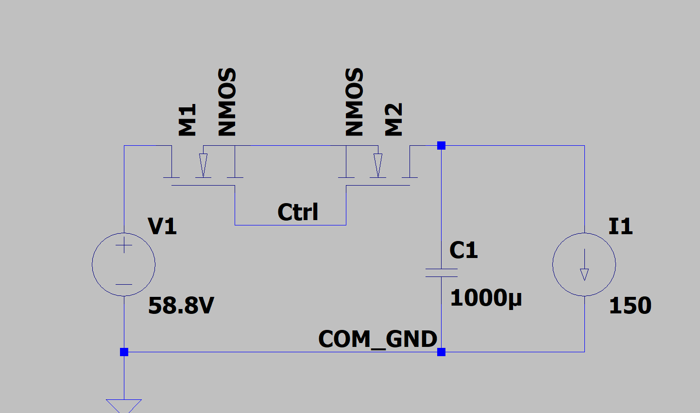
Imagine a battery pack with <=60VDC of maximum voltage and a load of up to 10kW of power(the PMSM inverter with the input capacitance of up to 1mF). The load is not always known - could be 100uF-1000uF input capacitance while the currents usually range from 20A up until 150A. The load is switched on/off using N channel Mosfets. Since there is no galvanic isolation present in the system peripheral communication interfaces(i.e. RS485/CAN) share the same GND as the load.

Approach 1) high side switch Switch the high side. Put FETs on the high side and control the "ctrl" net using gate drivers. The communication interface(RS485/CAN) is referenced to the "COM_GND" net.

Approach 2) low side switch Switch the low side. Put FETs on the low side and control the "ctrl" net using a 12V switch without gate drivers. However, in this case, the communication interface is referenced to the "COM_GND" net.

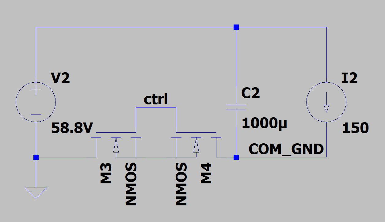
Note: Precharge circuit is present but omitted from the schematic

  1. Is there a superior architecture approach in this case?

  2. Could "Approach 2)" harm any of the components due to the ground reference loss?

History
Why does this post require moderator attention?
You might want to add some details to your flag.
Why should this post be closed?

1 comment thread

General comments (6 comments)
General comments
Olin Lathrop‭ wrote over 3 years ago

There is way too much hand waving here. Draw a block diagram, and define your terms. We don't know what you think a "LVD domain" and a "PMSM inverter" are. And what is "1.000,00 uF" supposed to mean? Is that really 1 uF to absurd precision, or some screwup with commas and points?

Olin Lathrop‭ wrote over 3 years ago · edited over 3 years ago

That's a bit better, but brings up other questions. Why are there two different FETs back to back for the switch? Where is the load? You mention communications interfaces, but none are shown in the schematics. What's the point of the current sources (I1 and I2 in your schematics)? You also have a regular ground, and "COM_GND". What exactly are these connected to outside of these schematics?

Andy aka‭ wrote over 3 years ago

Superior architecture: you don't need two series MOSFETs. What made you think you did?

2kind‭ wrote over 3 years ago

@AndyAka The reason behind having two series MOSFETs is to prevent charging of the battery through the body diode when the FET is on.

Andy aka‭ wrote over 3 years ago

@2kind - don't be silly - that only applies to an AC voltage source where the MOSFETs alternate at blocking. This is a DC application as in "battery".

2kind‭ wrote over 3 years ago

"the FET is on" - I see what I wrote now - it should be "the FET is off". I wouldn't call this silly, especially when the load is motor.