Communities

Writing
Writing
Codidact Meta
Codidact Meta
The Great Outdoors
The Great Outdoors
Photography & Video
Photography & Video
Scientific Speculation
Cooking
Cooking
Electrical Engineering
Judaism
Judaism
Languages & Linguistics
Software Development
Mathematics
Mathematics
Christianity
Christianity
Code Golf
Code Golf
Music
Music
Physics
Physics
Linux Systems
Linux Systems
Power Users
Power Users
Tabletop RPGs
Tabletop RPGs
Community Proposals
Community Proposals
tag:snake search within a tag
answers:0 unanswered questions
user:xxxx search by author id
score:0.5 posts with 0.5+ score
"snake oil" exact phrase
votes:4 posts with 4+ votes
created:<1w created < 1 week ago
post_type:xxxx type of post
Search help
Notifications
Mark all as read See all your notifications »
Q&A

Comments on How to protect RF switches from ESD?

Parent

How to protect RF switches from ESD?

+6
−1

Assume that I have some generic antenna connector, followed by a pi-filter/50ohm impedance matching components, then a DC blocking cap (as per the RF switch recommendations) and then a RF switch for split tx/rx semiduplex transceiver, as in this schematic:

antenna schematic

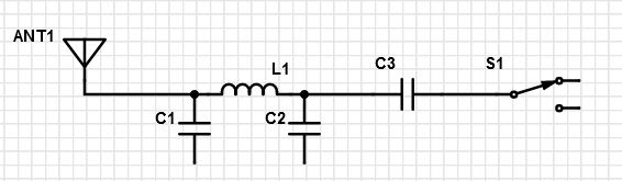
How do I best protect this RF switch from ESD coming in from human fingers touching the antenna connector? I need the highest ESD class (4) of the IEC61000−4−2, meaning 8kV contact discharge, 15kV air discharge.

I'm considering a specialized "ultra-low capacitance" TVS diode such as ESD8472 (rated up to 20kV), which is bidirectional.

Questions:

  • Is this TVS diode the way to go?
  • If so, where do I place it in this schematic? Directly on the antenna or somewhere else?
  • How to determine the suitable breakdown voltage? I'm assuming it should be based on the RF switch supply which is 3.3V.
History
Why does this post require moderator attention?
You might want to add some details to your flag.
Why should this post be closed?

2 comment threads

Hello Lundin. I think it would help if you can specify what is the general configuration of your syst... (2 comments)
Are you going for the formal IEC 61000−4−2 certification test? Sometimes passing a test it a harder ... (2 comments)
Post
+3
−0

Those are good questions, and I don't have a single definitive answer for them. I'd start with putting an appropriate TVS (or maybe separate diodes to ground and 3.3 V) between C3 and S1. My reason for clipping there is because then this gets to work against the impedance of the inductor.

Look carefully at the capacitance of the TVS or diodes, and reduce C2 accordingly. This is where separate diodes might be necessary if you can't find a suitable TVS that has less capacitance than C2 needs to be.

In the end, you need to test yourself. Fortunately, the high voltage discharge models are usually no more than a capacitor and resistor, so you can make your own with a high voltage supply. Several places I've worked over the years made jigs like that. At HP we called it the "fickle finger" test. Testing it yourself lets you do fast turn arounds, and gives you confidence you'll pass the real test at the certification company.


It sounds as we will need to run this in a simulator or we'd be fumbling around in the dark

Seems the opposite to me. You need some real experimentation. There are too many unknowns to allow sufficiently realistic simulation of high voltage transients. There are parasitic capacitances all over the place. Parasitic inductances also matter. Capacitors can be quite non-linear at high voltages, and leakage in various places may not be resistive anymore either. The biggest unknown is how exactly the RF switch input reacts to short term out-of-range spikes.

All in all, this is a case where you need to use experience, intuition, and something called a "brain". Let the new kid play with the simulator while you actually fix the problem the old fashioned way by doing some real lab work.

History
Why does this post require moderator attention?
You might want to add some details to your flag.

1 comment thread

Filtering makes things even more complicated (3 comments)
Filtering makes things even more complicated
Lundin‭ wrote about 2 years ago

Thanks for the feedback. It sounds as we will need to run this in a simulator or we'd be fumbling around in the dark :) In case of the tx path behind the switch, then this "pi-filter" is actually part of a larger Chebyshev filter which should be split across the switch like this according to the RF experts - I suppose it's because then it then also helps filtering in the rx path. So if these caps are changed, the whole filter needs changing, and it needs to match the PA which is of some peculiar "class E" type. Overall it's complex and I'm just acting as project manager/firmware guy trying to make a design review of what the RF engineers have proposed. I do suspect that we have ESD problems in the current design though, since the switches mysteriously get damaged intermittently. First we thought this was because of non-terminated trace stubs in the layout, but today I had a PCB with a cleaned up layout where the switch broke anyway.

Olin Lathrop‭ wrote about 2 years ago

Yup, that does smell like an ESD problem.

Lundin‭ wrote about 2 years ago

They also break in different ways. Some just are dead, conducting nothing. Others only work in one direction. And this latest one seemed to have shorted tx with rx with antenna. Which perhaps implies varied strengths of a ESD. Had it been some standing wave/impedance matching/reflection problem, I'd expect them all to break more or less in the same way since the tx power is constant. And in the rx direction, the switch should supposedly be able to handle a whole lot of out-of-band energy from other transmitters.