Comments on Ground pour on outer layers on 4-layer PCB
Parent
Ground pour on outer layers on 4-layer PCB
I'm designing a board that contains a cortex-M4 mcu working at 120MHz, and an ethernet bus with a wiznet chip that communicates with SPI.
The ethernet chip gives me a phy output that goes directly to a connector with internal magnetics.
All circuits are powered by a DC to DC buck converter.
The final product is a 4-layer board.
The stackup is:
Signals
Ground
Power
Signals
The board is one sided (every component is placed at the top layer).
All the traces are nicely routed on top with about 10 percent of them are at the bottom.
The inner ground layer is consistent across the whole board and it is not interrupted anywhere.
Every trace or pad that needs ground goes through a via to this layer.
The same happens with the power planes.
This is to minimise impedance.
The size of the board is 130mmx90mm.
The final step is whether I need to fill the empty space of the rest of the board (top and bottom) with coper ground pour (that will stitched to ground) or not.
I read that it is usually not needed in multilayer boards. However it is mostly useful to help manufacturers as it reduces etching time, less chemical waste, easier to manufacture etc.
Also, it reduces the twisting which is more useful in large PCBs although I'm not sure if my board is considered large. probably not.
Personally I'd like to leave it as it is without any ground pour on the outer layers but I'm concerned about manufacturability.
On the other hand if I try to fill the board will ground pour I'll have to stich it with vias that will probably need careful consideration on the placement.
What do we do in those cases?
Would it be better to have some lands of copper that is stitched well to the ground but not connected to any components pads?
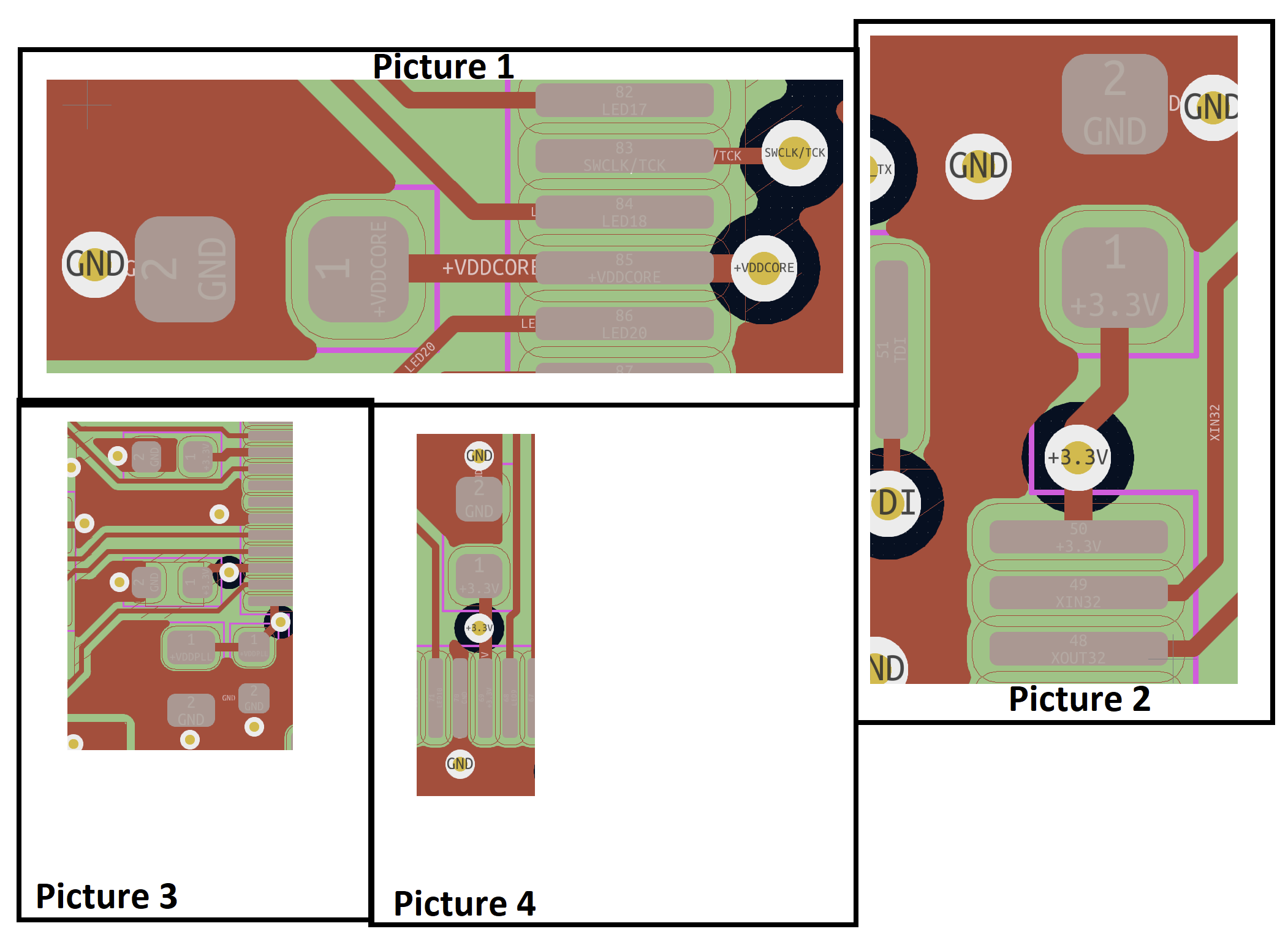
Regarding the grounding of the bypass capacitors: I'm posting a screenshot of how these capacitors are connected to the ground plane.
Post
I would not do deliberate ground pours on a board like that. It's relatively small, and not exceptionally high frequency.
I also wouldn't try to guess what effect or not it might have on the board fab process. I've put similar microcontrollers on larger boards many times and not had any issues like warping, or the board house complaining that I made things difficult. If you're really worried about this, talk to your board house. You will probably find that they don't care as much as you think. The most costly thing for them is probably a large number of vias, with the board geometry otherwise held constant.
Even if the board warps slightly, how does that matter? You have a small board, so it will probably be held with four screws in the corners. It can't twist when held that way. Would it really matter if the center of the board was out of the mounting plane by a mm? That's quite a bit, but you'd probably not notice anyway.
You mention layer 3 is a power plane. If you've got only one power supply, then it's OK to dedicate a plane to power if it doesn't cause hardship in routing the remaining signals. However, power planes are overrated for "ordinary" boards like yours. The capacitance between the power and ground layers isn't enough to absolve you of using bypass caps. Since the bypass caps will be there at each point of use of the power, what exactly do you think the power plane does for you? With a good ground plane and proper bypassing, there is little advantage to a power plane at your frequencies.
Every trace or pad that needs ground goes through a via to this layer.
That's bad. Your ground plane is now a center-fed patch antenna.
The ground plane is for solidly connecting the different parts of your circuit to the same ground potential. An uninterrupted ground plane also allows ground return currents to follow underneath the outgoing currents, thereby minimizing loop area.
However, the plane part does little useful for connecting the ground side of a bypass cap to the chip ground pin. A direct connection would be just as effective for bypassing purposes. But using a direct connection off the ground plane keeps the high frequency power currents generated by the chip off the ground plane, thereby not exciting the patch antenna.
Bypass caps should be directly connected and physically close to the chip power and ground pins. The high frequency power currents generated by the chip will run in this loop. You want to keep that loop small, and the currents away from everything else in the system. After connecting the bypass cap with its own deliberate traces, connect the bypass ground to the ground plane with one single connection. This is usually a via close to the ground pin. That still provides the solid ground reference to the chip, but keeps the nasty high frequency power currents locally contained.
I would argue that 500MHz and above would be the point where closely coupled power planes can begin to become as effective as high frequency capacitors at delivering power.
That's a reasonable point. At 500 MHz, a power plane close to the ground plane would start to have some positive effects. If it doesn't get in the way of routing other signals, then there is really no downside (although not a compelling upside either).
I'm not sure I understand your point about the ground plane being a center-fed patch antenna.
Think of how you would drive a patch antenna from circuitry on the patch. You'd run the driving RF across some piece of the patch.
Now consider what currents run across the ground plane when the bypass cap to a chip is connected to the chip ground pin by each having their own via to the ground plane. The chip is a high frequency current generator on its power feed. This current flows out the power pin, along some trace to the bypass cap, thru the cap, thru a via to the ground plane, across the ground plane, thru a via to the chip ground pin. The part of that loop where the current runs across the ground plane is basically the RF feed of the patch antenna you call a ground plane.
Do you mean that they should be connected to the ground pins directly using traces or local planes and connect all of it together to the internal ground plane?
A bypass cap should be connected to the power and ground pins of the chip it's bypassing with short and dedicated traces. The nasty high frequency current generated by the chip will flow over those traces. By making them dedicated traces, they can't flow anywhere else in the system.
Of course the chip still needs to be grounded. That should be done with a via to the ground plane close to the ground pin. The overall power return current will flow thru this via, and therefore across the ground plane to the power supply. However, the high frequency power current generated by the chip will stay local in the bypass cap loop and not flow across the ground plane. This keeps the ground cleaner and reduces RF power being fed to the patch antenna.
Another way to think of the same thing is that the bypass cap is the local shunt for the high frequency power currents generated by the chip. You want to keep those currents contained in a small loop, with little ability to go anywhere else in the system. With the ground net of that loop connected to the master ground in only one place, the bypass cap loop currents can't flow across the ground plane.
why you would not add a ground pour on top/bottom layers?
There are advantages and disadvantages. I would only do it if the advantages outweight the disadvantages. Disadvantages include:
- Can make routing harder.
- It's more to do, and therefore more opportunity to mess up.
- It takes engineering time, which is not free.
- The top and bottom ground-filled areas need to be regularly stitched to the real ground plane. If not, dangling ends can act like antennas and actually make things worse.
- Properly stitching a significant ground patch to the main ground plane requires a lot of vias. The number of vias goes with the area, not the linear dimension. These vias may add cost, can get in the way of good routing, and provide even more opportunity to make a mistake that requires a re-spin.
- For ordinary microcontrollers, there is little advantage. One full ground layer can be a significant help, but additional patches, especially on layer 1 when the ground plane is on layer 2, really don't do much for you.
6 comment threads

0 comment threads