Comments on Noise from oscillator on top layer to clock on bottom layer with VCC & GND layers between
Parent
Noise from oscillator on top layer to clock on bottom layer with VCC & GND layers between
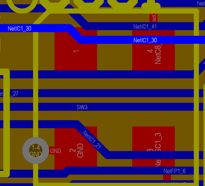
What effect does an oscillator potentially have on a SPI clk signal if the oscillator is on the top layer, with GND and VCC layer in between on a four layer board. I know running it on the same layer within a certain distance will have coupling effects that could cause noise and the 3W rule. I don't see people talking about different layers as much though. The clock is on the bottom like in the picture below. I know speed of oscillator and clock will likely determine if it will actually cause issues, but I am wondering about the general physics/practical noise that could be caused.
Post
What you are proposing may be okay (depending on other specifics of the design), but your proposed 4-layer PCB stack-up looks like a compromise. Clock is a high speed signal, and so is SPI depending on the edge raise time. Clock and SPI are on different layers: top and bottom. What acts as reference layers for these signals?
A high speed signal should have a reference plane layer next to it. A GND plane layer serves as good reference plane in theory and in practice. A VCC plane layer can serve as a reference plane in theory, but there are practical hindrances. If you want to route a signal through a via from the bottom layer which uses VCC plane as a reference to the top layer which uses GND plane as a reference, then you have to connect the reference planes near the signal via. How would you connect the reference planes if they are at different potentials? You would connect them through a coupling capacitor. But then you have to have a lot of these coupling capacitors, which isn't convenient.
As a result of the above considerations, there are two non-compromised options for 4-layer PCB stack-ups.
1 - high speed signals, sensitive signals
2 - GND plane
3 - VCC plane, other power distribution
4 - low speed and non-sensitive signals
If not enough real estate for high speed signals on the top layer:
1 - high speed signals, sensitive signals
2 - GND plane
3 - GND plane
4 - high speed signals, sensitive signals
If you find yourself hard pressed to do a 4-layer PCB with two GND planes, then consider a 6-layer PCB:
1 - high speed signals, sensitive signals
2 - GND plane
3 - VCC plane, other power distribution
4 - low speed and non-sensitive signals
5 - GND plane
6 – high speed signals, sensitive signals
That's a common stack-up for a 6-layer PCB, although not the only good 6-layer stack-up.
1 comment thread

0 comment threads