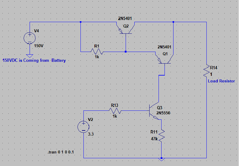
PNP Darlington pair as a current limiter
I am trying to analyse what is controlling the load current in the below Darlington configuration.
- Is it the base current of transistor Q3 which is controlling current through R14 / emitter current of Q2?
-
If it is, then is the maximum permissible load current is calculated by Ic(Q3) * Q1 beta * Q2 beta ?
-
From light load to maximum load, will all three transistor stay in the active region? For light loads , Q2 may get into saturation region I suppose.
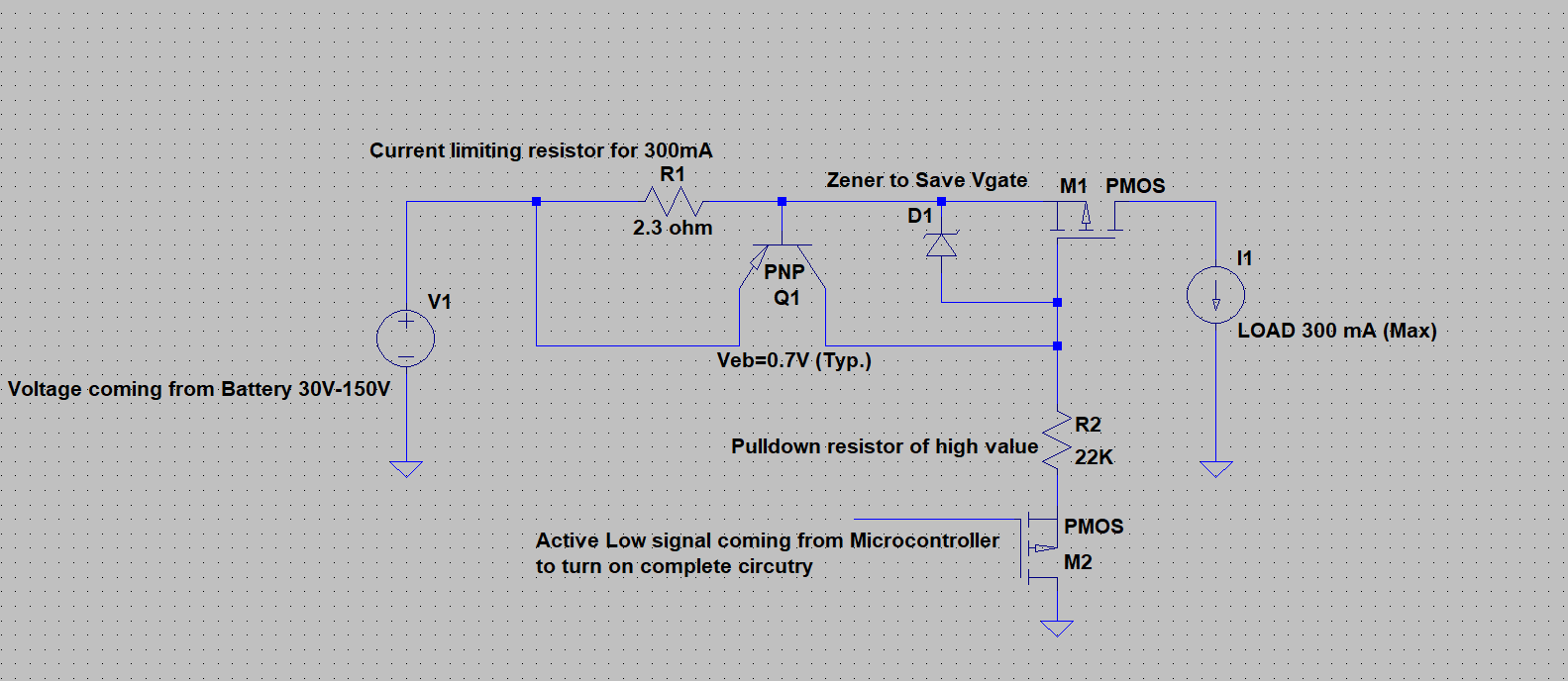
EDIT : Alternate circuit to achieve the same functionality
are there any drawbacks to use this circuit ?
1 answer
Follow the current.
Q3 is a controlled current sink. Whatever voltage is applied to its base appears across R11 minus the B-E drop. That voltage on R11 causes a particular current to flow. That current obviously flows out of the emitter of Q3. Due to the transistor's gain, most of that comes from the collector, not the base.
To first approximation, Q3 sinks V2 minus a junction drop, divided by R11. Note that this is fairly independent of the voltage on the collector of Q3.
Q1 and Q2 act like a single high-gain PNP transistor with a high saturation voltage. Just like a regular PNP, the maximum collector current is the base current times the gain. In this case the gain is roughly the gains of Q1 and Q2 multiplied together.
So roughly at first approximation, the maximum load current this circuit can provide is V2 minus the B-E drop of Q3, divided by R11, times the gain of Q1, times the gain of Q2. If the load doesn't draw this amount, then the darlington transistor saturates, as would any BJT in its place.
Note that if the darlington doesn't saturate, then there can substantial voltage across it, which causes significant power dissipation, which might destroy Q2.
This was all assuming reasonable positive voltage from V3. It's not clear what that is, and what "150" is supposed to mean. We do engineering here. Hand waving of undescribed dimensionless quantities is not appreciated, and may result in downvoting and/or closing of questions with such issues in the future.
What's the purpose?
The above describes how the circuit works, but it's not clear what you are actually trying to accomplish. If your goal, for example, is to make a current source, then this is not a good circuit.
Q3 makes a reasonably good voltage-controlled current sink, but the final load current limit depends too much on the gains of Q1 and Q2. Those can vary considerably between devices, even from the same manufacturing lot. The gains also vary as a function of temperature, collector current, and other parameters it's hard to know the effect of.
The purpose of this circuitry is to limit current through load resistor for 1 A when 150 Volts appears on the car battery . Input Voltage from Car battery varies from 30V -150V .
Then you really don't want to use this topology. It will be very difficult to set the current to any one value with any kind of accuracy. Another really big problem is the power dissipation. At 1 A, the load will only drop 1 V. With 150 V in, the pass element will drop 149 V. That means it will dissipate 149 W. That's well beyond what a single transistor with good heat sink can dissipate. Even if it could, it would take a lot of space and cost a lot.
You haven't told us what this is really for, but I would look into a buck switcher run to control the current directly. You need a small current sense resistor somewhere, but that doesn't need to drop more than a few 100 mV. The controller of the buck switcher uses that as feedback to regulate the current.
Second circuit
Your new circuit has at least somewhat predictable current regulation. You are using the B-E junction of a PNP transistor as the voltage reference to compare the voltage across a current sense resistor against. That works as long as you are OK with the various inaccuracies and temperature dependencies.
Note that with 2.3 Ω sense resistor against a 700 mV reference, the current will be regulated to 300 mA, not 1 A.
However, the real problem is that the high power dissipation is still there. No matter what transistor or other pass element you use, a linear regulator dissipates the voltage it drops times the current thru it. That could be nearly 150 W if the current is really supposed to be regulated to 1 A. If the 300 mA value is to be believed, that's still 45 W. 45 W might be doable if you get the right transistor with a large heat sink and forced air cooling. A buck switcher controlled to regulate current will be significantly smaller, cheaper, and require much less heat management.
R1 (1K) what major role does it play in first circuit ?
It is probably to make sure Q2 doesn't come on due to leakage of Q1. It guarantees that Q1 is well into deliberate conduction to cause Q2 to turn on. R1 also makes Q2 turn off faster.
Those are some effects. It's difficult to say what the designer intended.

1 comment thread