DAC controlled high side current source.
I'm designing a high side current source that can be controlled with a Digital-to-analog and can source up to 100mA with voltage supply up to 36V.
By high side I mean one side of load will be always grounded. Below you can see a reference design of a such circuit.
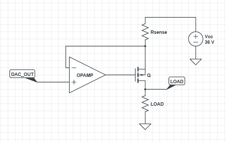
In the design above the main issue is that the output of the DAC needs extra amplification and also the output of the OP Amp needs to go up to V+ in order to put MOSFET Q to cut-off region.
Which means the Op Amp needs to have a rail-to-rail output at best and also a wide operating voltage range that can go up to +36V.
So, I was thinking maybe to do some modifications so I can replace the op amp with something that can work with much lower voltage. Perhaps with the same voltage as DAC works.
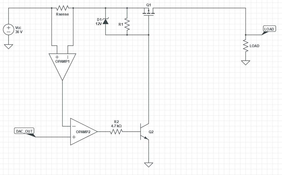
The OPAMP1 could be a generic differential amplifier or even better an integrated current sense IC that will result in a current to voltage conversion. This will feed the OPAMP2 who can work at the same voltage as the DAC IC.
When the current goes up, OPAMP1 voltage rises, OPAMP2 pulls its output down to zero, Q2 stops contancting VGS of Q1 decreases and limits the current of the drain-source channel.
The question:
I'm very concerned that something will not work regarding the mosfet control circuitry, especially the Q2. Is there something that needs to be done in order to achive smooth control of the current?
The longer I see the circuit the more confused I get and I'm starting to believe that the gate will start to oscillate.
Design Specifications:
- 0.1% accuracy on the output current.
- Accpetable voltage drop across power elements up to 8V.
- Lowest voltage across load in zero setpoint must be closest to zero possible.
- Operating voltage range 12V to 36V
1 answer
The following users marked this post as Works for me:
| User | Comment | Date |
|---|---|---|
| DeadMouse | (no comment) | Mar 12, 2022 at 21:48 |
It appears you want a positive current source with the following specs:
- 0 to 28 V compliance range.
- Up to 100 mA, adjustable via 10 bit or more digital value.
- 36 V supply is available.
- The dissipation from a linear pass element is OK.
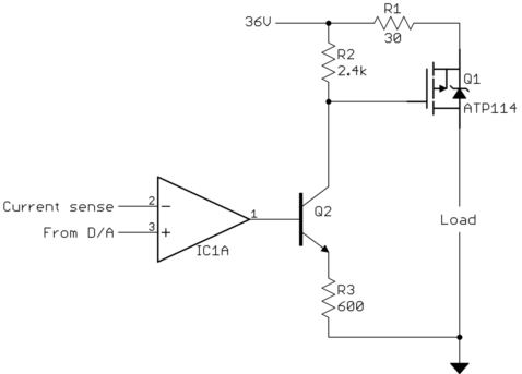
The large headroom at the high end allows for easy current sensing. A 30 Ω resistor, for example, would provide a 0 to 3.0 V signal. Note that it would dissipate 300 mW at 100 mA, so should be a "½ W" type at least.
At 100 mA and 0 V out, a total of 3.6 W will be dissipated. The sense resistor will take some, but the pass transistor will need to dissipate most of that. 3.6 W is quite doable with the right power transistor and heat sink. Something in a TO-3 case can handle this easily. A TO-220 case should also be doable with the right heat sink. Those two cases should provide plenty of options to find a suitable transistor.
So at this point we have the 36 V supply, a 30 Ω or so current sense resistor, and P channel power FET. The drain of the FET drives the high side of the load, with the other side of the load connected to ground.
The question now is how to drive the FET gate. At this point, there are a number of possible topologies.
One way is to use a diff amp to make a ground-referenced sense voltage, then have the controller also be ground-referenced. This is basically what your second schematic shows, except I would use the output of the opamp differently:
This at least makes the FET gate voltage roughly linear with the opamp output. Unfortunately, the function of gate voltage to output current is still rather non-linear, and can lead to instability in parts of the operating range. Put a small cap immediately between the opamp output and its negative input. Start with a few 10s of pF, and increase until everything is stable, then double it. The "Current sense" signal will also need some impedance for the cap to work against.
Another possibility is to use a 12 V negative regulator to make 12 V below the 36 V supply. An opamp can run from that 12 V and drive the FET directly. Now there is no need for a diff amp to create a ground-referenced current sense signal.
The problem then becomes getting the desired current signal to the high side. A similar circuit to what I show on the low side, above, could work. It translates the ground-referenced D/A output to a current, which is then independent of voltage.
Yet another option is to put the D/A on the high side too. That simplifies all the analog circuitry. Only the digital signals into the D/A need to be transferred to the high side. That can be done with opto-isolators, or more voltage to current sink converters like Q2 and R3 above.
I did not understand the negative regulator part you're talking about. How would that work?
Here is an outline of the topology:
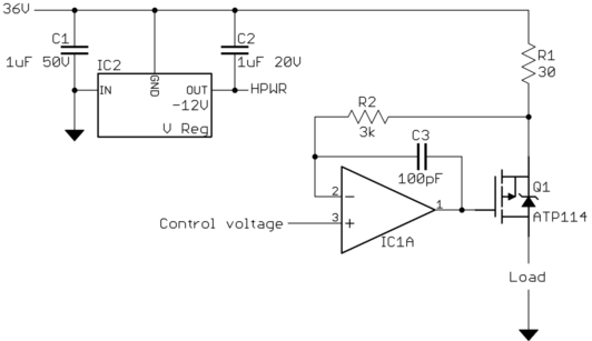
IC2 is a negative voltage regulator. Note that its ground input is connected to the 36 V supply. It will therefore make a clean -12 V relative to the +36 V supply, so about +24 V nominal. However, this supply is set up to sink current, not source it. It is a true negative supply relative to the 36 V rail. The purpose is to have a means of powering "high side" circuitry.
In this case, the opamp would be powered from 36V and HPWR. The advantage is that now the opamp can directly connect to the current sense voltage and the FET gate. Note C3 to provide stability, and R2 to provide some impedance for C3 to work against. The price for this stability will be lower bandwidth, but you haven't specified any bandwidth requirement.
The output current will be directly proportional to the 36 V supply minus the control voltage. Put another way, this control voltage is high-side referenced. As I said earlier, you can produce this in analog from a low side control signal, or include the D/A in the high side circuitry and only have to get digital signals controlling the D/A from the low side to the high side.
Depending on what else the digital controller has to do, perhaps you can float the whole thing on the high side.
What does R2 really do here?
R2 allows C3 to do its job. C3 provides some immediate negative feedback at high frequencies around the opamp to help with stability. Depending on the opamp, it may not be required at all.
Now imagine that the negative input of the opamp were driven with a 0 impedance source. C3 would become irrelevant. One way to look at it is that C3's impedance forms a voltage divider with the impedance driving the negative input. If that second impedance is 0, then that voltage divider has a gain of 0. Some finite impedance is needed in driving the negative input so that some portion of the signal thru C3 also contributes to the overall negative input voltage.
Another way to think of this is that the signal from the output of the opamp gets high pass filtered onto the negative input, with the rolloff frequency set by C3 and R2. In the example above, that rolloff frequency is 530 kHz. That's about the frequency where the feedback thru C3 starts of have an effect. The point is to make that frequency lower than where the system becomes unstable. By lowering the loop gain at higher frequencies, the effects of inevitable phase shift at higher frequencies are mitigated to keep the system stable.

3 comment threads