Isolated Digital Input - Overvoltage protection
I am trying to build an active-low digital isolated switch capable of withstanding 32VDC voltage without creating any damage to the system.
This is the snapshot of the circuit not fulfilling the requirement:
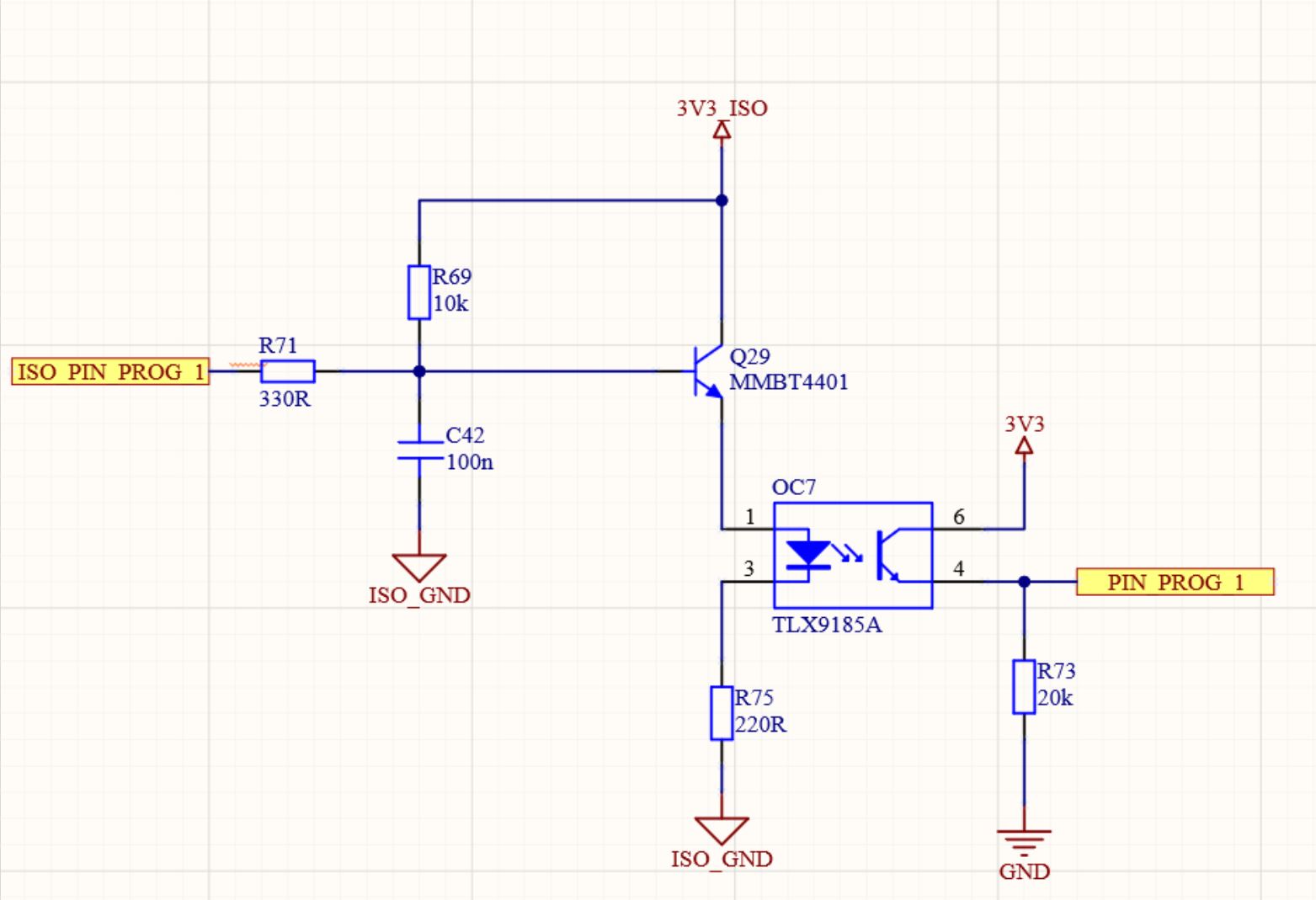
"ISO_PIN_PROG_1" will be connected to the switch which will tie to the ground and causing the base of the Q29 to go below 0.7V hence cutting off the OC7.
"PIN_PROG_1" will be connected to the MCU input.
If there is a 32V applied by the accident on "ISO_PIN_PROG_1" this would cause problems with the circuit as is. How could I properly solve it?
-
Step 1: Since 3V3_ISO would be LDO driven I would probably add a diode with the anode connected to the LDO output and a cathode connected with the LDO input to prevent the LDO to have output higher than the input. Based on my experience they tend not to love that. I haven't post that because I haven't yet designed the power stage.
-
Step 2: Add Zener regulator at i.e. 12V with a properly dimensioned resistor and add one more resistor in series with Q29 base to limit the current - does it need to be limited because there is a limit how high Ic of the Q29 could be in full saturation? I believe it should because it won't be in the forward active region anymore.
I may be stuck having multiple unknowns and not being really secure whether this is the right topology for the task and whether I am addressing the problems correctly so your help would be kindly appreciated! Thanks as always!
Further clarifications ——————————————————————————
When input is left floating opto’s diode is forward biased as seen on the schematic. When input is low, the opto should be off therefore “PIN_PROG_1” should be high. That is really all in terms of usual usage. However, there is a chance that someone would connect 32V max on the input and without adding any support the circuit shown would be damaged. Proper operation during the event is not needed - so when between 3V3 and 32V on the Q29 base circuit and PSU should not be damaged, output of it is less important. Snap on action is not required. Esd protection is important. Input impedance should be high.
3 answers
You are accessing this answer with a direct link, so it's being shown above all other answers regardless of its score. You can return to the normal view.
UPDATED. based on clarification to original question.
To be clear, just an idea, not tested for this situation!
It is abusing the V_I_L margin on the 3.3V CMOS input, so series diode should be schottky...
To summarize, it seems you want a circuit that will detect an input voltage high/low with a threshold somewhere between 0 and 3.3 V, must operate correctly with 0-3.3 V input, but must tolerate input up to 32 V. Snap action (hysteresis) is not required. An opto-isolator is to be turned on when the input is high, and off when low. The input impedance of this detector circuit is unspecified, so we can draw whatever current is convenient for us. Response time is also not specified. Apparently, inverting when the opto is driven is also acceptable.
Here is a circuit that meets these specifications, with the opto being on when the input is high:
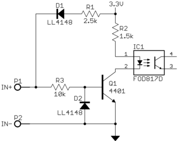
Theory of operation
Q1 being on turns on the opto. Q1 is turned on when the IN+ input is high. R3 limits the base current thru Q1. R1 pulls the input high when it is left open. D1 blocks reverse flow onto the 3.3 V supply when the input goes above 3.3 V. D2 is not necessary according to the specification provided, but is a good idea for robustness. Stuff happens. D2 protects the circuit from negative input voltages that would cause too much reverse voltage across the B-E junction of Q1.
Part values
The diodes are easy because pretty much anything is good enough. I show the 4148 because that's my jelly bean part to use in such cases unless there is a reason not to. With at least 75 V reverse voltage and 100 mA forward current, no limits are being pushed.
R2 controls the current thru the opto when it is on. 1 mA is enough current for this kind of opto. Figure Q1 eats up 200 mV when in saturation, and the LED about 1.2 V. That leaves 1.9 V across R2. (1.9 V)/(1 mA) = 1.9 kΩ. 1.5 kΩ is a common value that leaves a little margin.
R3 needs to supply enough base current when the opto is supposed to be on. We've already said that we want 1 mA of opto current. Let's say we want to be able to use just about any transistor, so require a minimum gain of only 25. That means we need only 40 µA of base current at whatever threshold voltage should be considered "high". Using 1.5 V as the threshold voltage, and figuring 700 mV for the B-E drop of Q1, leaves 800 mV across R3. (800 mV)/(40 µA) = 20 kΩ for the maximum R3 can be. The common value of 10 kΩ will therefore work nicely with plenty of margin.
R1 is the pullup that keeps the input high when nothing is connected. If a mechanical switch is ever used to hold the input low, we want some minimum wetting current. I figured the input should source a minimum of 1 mA when held at ground. Assuming 700 mV across D1, that leaves 2.6 V across R1. (2.6 V)/(1 mA) = 2.6 kΩ maximum. The common value of 2.5 kΩ leaves a little margin.
Over-Voltage
This circuit must survive with the input has high as 32 V. When that happens, D1 is reverse biased, so D1 and R1 can be ignored. The base current of Q1 will be (31.3 V)/(10 kΩ) = 3.1 mA, which is nowhere near pushing any limits of Q1. The dissipation of R3 will be (31.3 V)2/(10 kΩ) = 98 mW. A 0805 package or large can handle that without issue.
Under-Voltage
Although it wasn't specified, it would be good to safely allow some negative voltage on the input. D2 will clamp the base voltage of Q1 to a safe level. The issues will be the currents thru, and therefore the dissipation of R3 and R1. Clearly, R1 will have the higher dissipation, so let's see how much negative voltage can be tolerated if R1 can dissipate 125 mW.
Sqrt((125 mW)(2.5 kΩ)) = 17.7 V. Considering that the right end of R1 is at 3.3 V, and the drop across D1, this threshold is reached with an input voltage of -15.1 V. We could therefore quite comfortably spec this circuit to have an absolute minimum input voltage of -12 V. At that voltage, there will be a drain of 2.5 mA on the 3.3 V supply. That's fine since no supply current limit was specified.
A different circuit
Here is a circuit that also meets your specs, but this one keeps the opto off when the input is floating or high, and on when driven low:
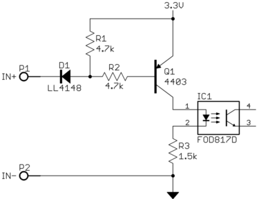
This is better if the input will be mostly high or open, and you want to sense the occasional low level.
Theory of operation
When the input is left open, it is pulled high by R1. This keeps Q1 off. Driving the input low draws current from the base of Q1, turning it on. That turns on the opto.
Part values
R3 serves the same purpose as before, and has the same value. If the saturation voltage of Q1 is 200 mV, and the LED drops 1.2 V, then there is 1.9 V across R3. (1.9V)/(1.5 kΩ) = 1.3 mA. Even 1 mA is sufficient for this opto to be able to work against a 10 kΩ pullup or pulldown on its output at common logic voltages.
The resistors were sized to source about 1 mA of wetting current when the input is shorted to ground. This is useful if a mechanical switch is tied between IN+ and IN-. Figure D1 and the B-E junction of Q1 each drop 700 mV. When the input is shorted to ground, that leaves 2.6 V across R1 and 1.9 V across R2. The current thru R1 is (2.6 V)/(4.7 kΩ) = 553 µA, and thru R2 is (1.9 V)/(4.7 kΩ) = 404 µA, for a total of 957 µA being sourced by the input when held at ground.
Threshold voltage
Even if Q1 had infinite gain, the input needs to drop about 1.4 V below the 3.3 V supply to bias D1 and the B-E junction of Q1 before any appreciable current flows. This means the upper limit of the threshold voltage is about (3.3 V) - (1.4 V) = 1.9 V.
Let's say that in the worst case Q1 only has a gain of 25 and that 1 mA is required thru the LED for the opto to be on. That means (1 mA)/25 = 40 µA of base current is required for guaranteed on operation. The voltage across R2 will therefore be (10 kΩ)(40 µA) = 400 mV. Making the same assumptions about the voltage drops of D1 and the B-E junction of Q1, this comes out to an input of 1.5 V.
The switching threshold is therefore somewhere in the 1.5 to 1.9 V range. This is from 46% to 58% of the 3.3 V supply.
Over-voltage
The absolute maximum input voltage comes from the reverse voltage capability of D1. This is easily 75 V, with some 4148 diodes specified to 100 V, plus the 3.3 V of the supply.
Under-voltage
The absolute minimum input voltage is limited by the dissipation of the resistors. It should be obvious that R1 is the limiting factor, since R2 has about 700 mV less across it. Using 125 mW maximum dissipation as before, the voltage across R1 can be sqrt((125 mW)(4.7 kΩ)) = 24.2 V. Taking into account the supply voltage and the drop across D1, that means the input can't go below -21.6 V. -20 V absolute minimum might be a good spec.
Let's look in detail what happens with -20 V input, which is what we would specify as the absolute minimum. The current thru R1 will be (22.6 V)/(4.7 kΩ) = 4.8 mA, and thru R2 (21.9 V)/(4.7 kΩ) = 4.7 mA, for a total input current of -9.5 mA. Q1 will clearly saturate, so there will also be 1.3 mA thru the LED. The total supply current is (4.8 mA) + (4.7 mA) + (1.3 mA) = 10.8 mA. This is acceptable since no current limit from the 3.3 V supply was specified.
The dissipation of R1 will be (22.6 V)2/(4.7 kΩ) = 109 mW.
Step 1: Since 3V3_ISO would be LDO driven I would probably add a diode with the anode connected to the LDO output and a cathode connected with the LDO input to prevent the LDO to have output higher than the input. Based on my experience they tend not to love that. I haven't post that because I haven't yet designed the power stage.
Indeed, this is common practice and does help saving the LDO. Normally I'd pick a schottky with high enough reverse voltage, to minimize the voltage difference between LDO input and output. However in this case, 32V is likely far too high input for the LDO (?) depending on type.
If you have no reason to suspect lots of EMI etc, you shouldn't need galvanic isolation, it makes the BOM expensive. Even with expected EMI, then normally it should suffice with a TVS together with some current limiting resistor, to take the brunt of the load in case some high voltage is applied by accident.
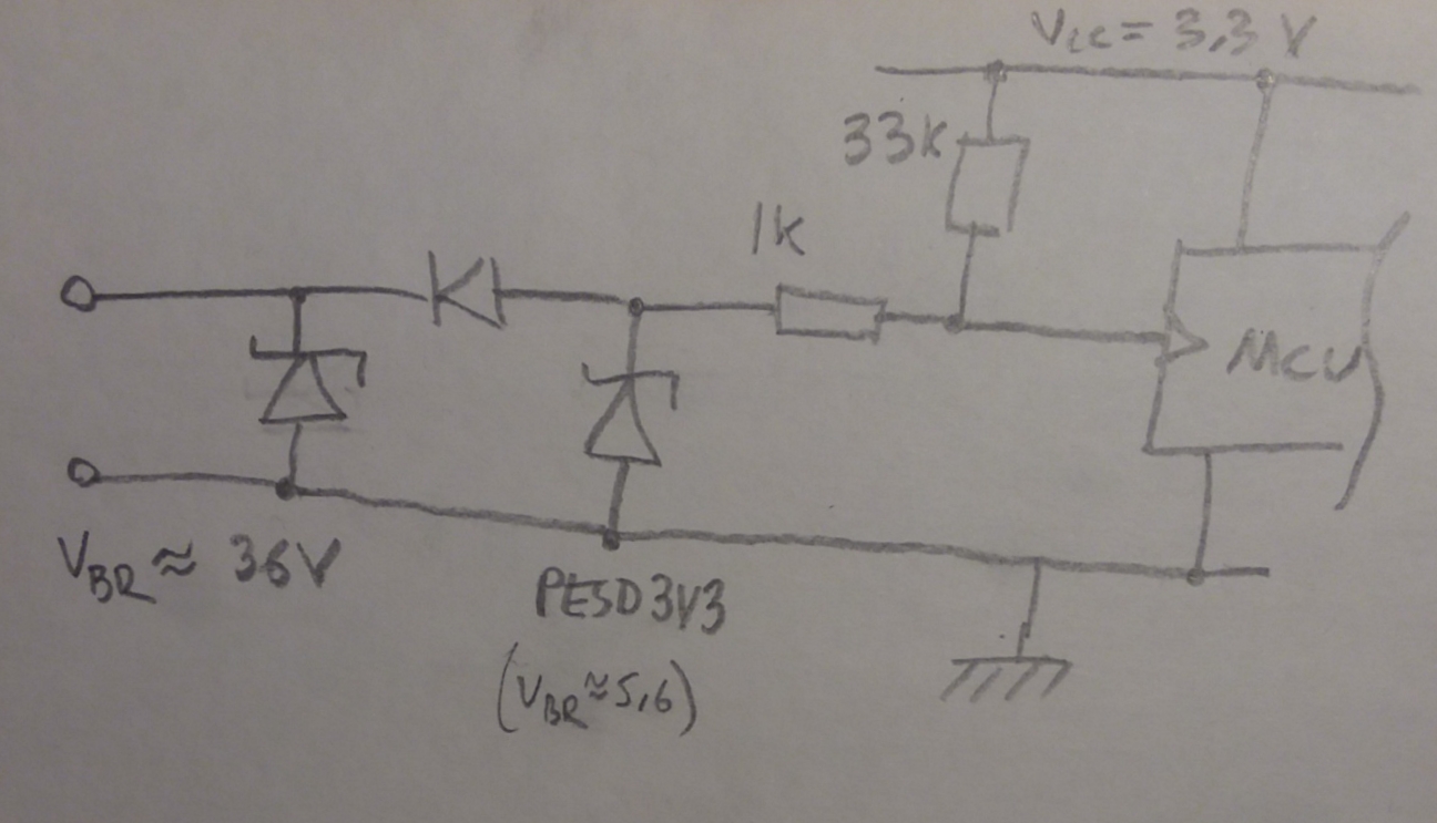
I'd get rid of the BJT, LDO and optocoupler and just add some protective diodes, one towards ground and one towards the voltage you want. Something like this:
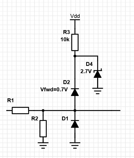
- TVS optional directly on the input (not drawn).
- Vdd is some known high voltage you've got access to, like 24VDC.
- R1 is some high ohm current limiter >10k.
- R2 optional if you need voltage divider
- If some high voltage is applied then you lose 0.7V across D2 and the rest across the zener. You end up with ~3.4V that you can safely connect directly to a 3V3 MCU etc.

1 comment thread