What is a good PCB-layout?
I am an electrical engineering student and I just finished designing an ECG-amplifier circuit. Here is the schematic: -
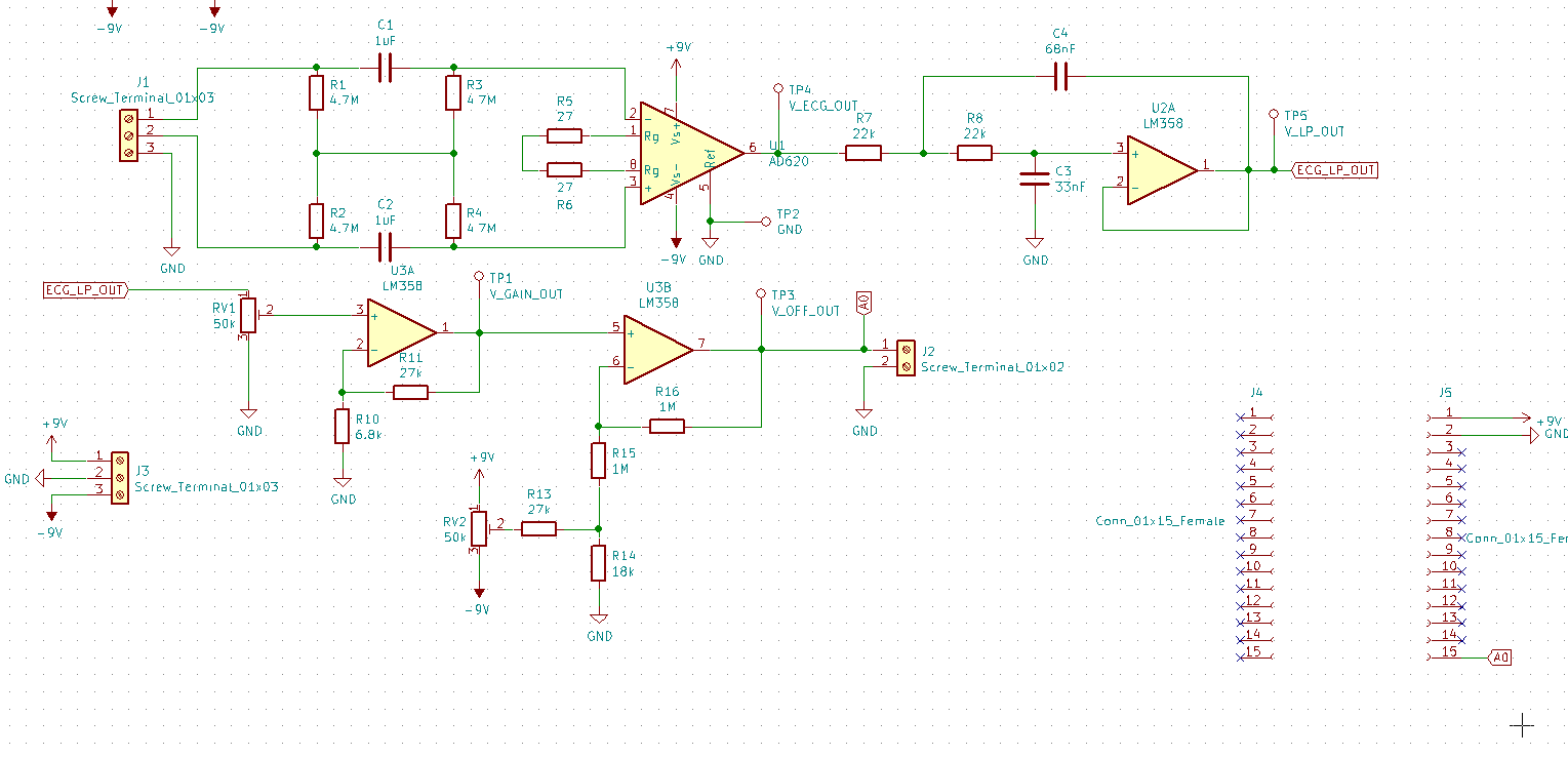
It is fairly simple. Initially, there is a 1st order highpass filter. Then, a differential amplification stage with AD620N in-amp followed by a Sallen-Key 2nd order lowpass filter. Finally, a gain and offset stage. The two female pin-header connectors (J4 and J5) are for plugging in an esp8266 module to sample the processed signal with its ADC. There are also some test points and some screw terminals.
I have also designed and ordered a PCB for this circuit here:
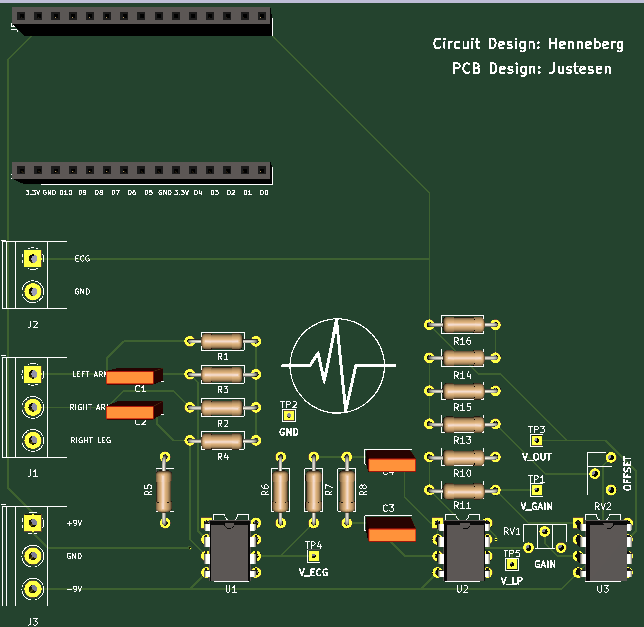
The PCB is 100x100mm, has 2 layers, and it only uses THT-components. The +9V and -9V are connected through traces to the amplifiers, and I use 1 GND plane.
Questions: I'm new to PCB-design and I don't have a feeling for what a "good" design is. Have I made some big "no-nos"? Is there a standard for placing components that's a good idea to follow? Where is it a good place to start with the PCB-design? Should I go from left to right following my schematic and wire components accordingly (that's what I have done)? Is this a poor design?
1 answer
I have also designed and ordered a PCB
It seems rather pointless to ask after you've already ordered the board.
only uses THT-components
That's just plain silly. This is the kind of thing that you might see from a clueless hobbyist, but is totally unacceptable from an electrical engineering student. Thru-hole components can still be useful for those plug-in breadboards, but don't design a PCB for them.
SMD components are smaller, more available, provide wider part selection, cheaper, easier to route boards for, and easier to physically work with. An SMD board also has the advantage of not making you look like a clueless weenie when showing it to others that know anything about EE.
Where is it a good place to start with the PCB-design?
Answering this really requires a whole book, so I'll just give a few pointers.
I usually start with placing mounting holes in the corners at least. Then place external connections on the edges close to those mounting holes. The external connections will get physically abused, so you want them to be as solidly held as possible.
Roughly locate those connections according to how they will be used. If the user will frequently connect/disconnect some signals, place their connectors at the front of the board. The programming and debugging header can go in the back so that it's out of the way during normal operation. Consider the flow. Input signals at left and output signals at right can make sense, for example.
After placing the parts that will cause mechanical stress, you may want to add mounting holes.
Decide how many layers the board will have. For a simple board that you can make large enough, two layers is often good enough. With the components on top, you can try to leave the bottom layer to be mostly a ground plane. Most of the interconnects will be on the top with occasional short "jumpers" in the bottom layer because it's impossible to route a circuit in a single layer in the general case.
If there are sensitive signals or reliability and signal integrity is more important that build cost, use four layers and reserve one for a board-wide ground plane. This would normally be layer 2, since most of the signals will be in layer 1.
Ultimately you want good routing so that signals are reasonably direct, power supply feeds low impedance, etc. However, good routing starts with good placement.
Start with critical components with lots of interconnects. In your case, that would be the opamps. I'd probably place one opamp temporarily somewhere in the middle, then incrementally place its closely-connected components around it to make the connections as short and easy as possible. Place the bypass caps first, then the remaining immediate components around the opamp.
This results in one clump of components around an opamp. Now you can move that whole clump around as needed. You can create several independent clumps like that, then place the clumps relative to each other according to how they are interconnected. Note that clumps can be placed off the board initially, then moved onto the board as a single unit later.
Think about the grounds and the return currents thru the ground carefully. The bypass cap connections should be direct and not go across the ground plane. Connect the ground of each chip to the master ground plane in a single point.
In your case, you don't really need a ground plane for radiation reasons. You don't have high speed signals, but you do have very low level signals. Make sure that power supply return currents don't cause offsets in the signals. This can be a reason to use four layers instead of two so that you have a solid plane for the ground.
I think your circuit can be routed in two layers, but if this were a professional project I'd use four layers unless it is a high-volume low-cost product. I can't imagine an EKG being that, though. There is so much expense in any medical product, that trying to cut cost by using two layers instead of four in a small internal board is ridiculous. A little lower noise and overall robustness is far more important that saving a dollar on a board in a $5,000 medical product that will only ever have 3000 made. The extra engineering time would probably exceed the savings anyway.
In your case in a learning environment, two layers may make sense. You don't really have a space constraint, it will be easier to edit the board during debugging, and slightly more noise isn't a big deal since you're presumably not creating a real medical device.
Someone wrote in a comment:
Through-hole is the only sensible choice if you have zero experience with soldering.
I totally disagree. SMD is easier to solder than thru hole. The thru hole procedure is:
- Insert the leads thru the holes.
- Bend the leads a little on the bottom so that the part doesn't fall out when the board is flipped.
- Repeat steps 1-2 a few more times so that several parts are now sticking thru the board.
- Flip the board over and solder the leads.
- Clip off the unused parts of the leads.
SMD is easier:
- Flow a little solder on one of the pads.
- With tweezers, hold the part in place.
- Melt the existing solder from step 1 to solder down that pad.
- With the part now reasonably held by the first pad, go around the part and solder the remaining pads.
- Go back and check the first pad. Maybe add a little solder.
Notice that SMD doesn't require flipping the board over, and lets you work on each part sequentially to completion. You can do the latter with thru hole too, but the process is less efficient than inserting several parts, then soldering in batches.
I have done plenty of soldering both ways. Not only is SMD easier to build a board to start with, but it's also way easier to change parts later.

2 comment threads