Communities

Writing
Writing
Codidact Meta
Codidact Meta
The Great Outdoors
The Great Outdoors
Photography & Video
Photography & Video
Scientific Speculation
Cooking
Cooking
Electrical Engineering
Judaism
Judaism
Languages & Linguistics
Software Development
Mathematics
Mathematics
Christianity
Christianity
Code Golf
Code Golf
Music
Music
Physics
Physics
Linux Systems
Linux Systems
Power Users
Power Users
Tabletop RPGs
Tabletop RPGs
Community Proposals
Community Proposals
tag:snake search within a tag
answers:0 unanswered questions
user:xxxx search by author id
score:0.5 posts with 0.5+ score
"snake oil" exact phrase
votes:4 posts with 4+ votes
created:<1w created < 1 week ago
post_type:xxxx type of post
Search help
Notifications
Mark all as read See all your notifications »
Q&A

When and where to use vias in an IC design layout

+3
−1

I am learning IC design layouts using Cadence Virtuoso and now I got stuck with the concept of using vias. The question is when and where to use it? I am attaching the schematic of my inverter tutorial
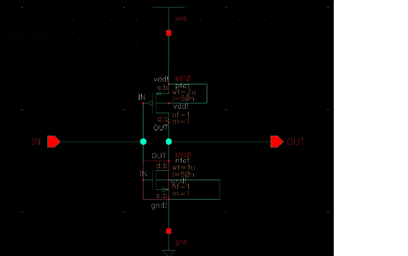
 here and layout here. Also herehere is the zoomed screenshot where vias are used for input and output pins. On the top and bottom we have Vdd and Gnd.The blue rectangle is the M1 metal layer and the purple is M2 metal layer.The dotted rectangle is the n-well which has pmos in red rectangle and in the below section we have nmos in red rectangle. The thin green rectangle which goes across the pmos and nmos is the poly. The input pin has both a contact and a via, whereas the output pin has only a via. Could you please guide me like when to use a via and where and also if there are more pins in a different design how should I analyse in having vias.

History
Why does this post require moderator attention?
You might want to add some details to your flag.
Why should this post be closed?

0 comment threads

1 answer

+1
−0

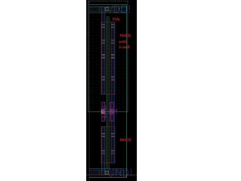
Vias are used to move up in metal layers. The contacts of the transistors can be directly connected with metal 1, but if you want to use higher metal levels, you move up to them with vias.

For example, if you use M1 (metal 1) and you need to cross another M1 trace that does not belong to your node, then you need to avoid it. You could use a via to M2 to avoid this trace.

Another very good reason to move up in metal layers is that, at least in deep submicron technologies, the higher metal layers have less resistivity than the lower ones.

For instance, I have experience with a particular technology where a few tens of micrometers can easily amount to a few hundreds of ohms, while higher metals can be only few ohms.

This means that metal layers also have their applications within a design. For an analog design, lower metal layers can be used to wire up static logic circuits (such as enable bits). In those cases, a few 100 ohms of wire typically doesn't matter, speed or a few 10s of mV are not important. On the other hand, higher metal layers can be used to wire up the amplifier itself, as you certainly don't want to be inserting parasitic series resistors on your nodes. Otherwise, you might degrade your amplifier's performance in a post-layout simulation.

History
Why does this post require moderator attention?
You might want to add some details to your flag.

0 comment threads

Sign up to answer this question »